HMC496LP3 / 496LP3E
v05.0811
11 - 1
Features
The HMC496LP3 / HMC496LP3E is suitable for
various modulation systems:
Wideband RF Frequency Range
High Carrier Suppression: 34 dBc
• Fixed Wireless or WLL
Very Low Noise Floor: -157 dBm/Hz
• U-NII Radios
Low LO Power: -3 to +6 dBm
• 802.11a & HiperLAN WLAN
Differential or Single Ended LO Drive
• C-band Microwave Radios
Single Low Current Supply: +3.0V@ 93 mA
E
Typical Applications
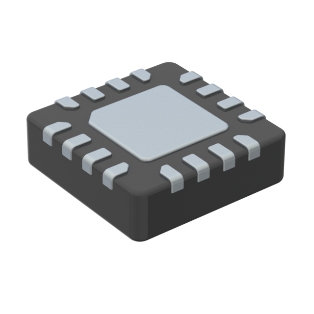
3 x 3 mm QFN SMT Plastic Package
General Description
T
Functional Diagram
B
S
O
LE
The HMC496LP3 & HMC496LP3E are low noise
Wideband Direct Quadrature Modulator RFICs
which are ideal for digital modulation applications
from 4 - 7 GHz including; WLL, U-NII, WLAN &
microwave radios.
Housed in a compact 3x3
mm (LP3) SMT QFN package, the RFIC requires
minimal external components & provides a low cost
alternative to more complicated double upconversion
architectures. The RF output port is matched to 50
Ohms with no external components. The LO requires
-3 to +6 dBm and can be driven in either differential
or single-ended mode while the Baseband inputs
will support modulation inputs from DC - 250 MHz
typical. This device is optimized for a supply voltage
of +3V @ 93 mA and will provide stable performance
over a +2.7V to +3.3V range.
Electrical Specifications, See Test Conditions on following page herein.
O
modulators - direct quadrature - SMT
11
SiGe WIDEBAND DIRECT
MODULATOR RFIC, 4 - 7 GHz
Parameter
Min.
Frequency Range, RF
Output Power
-1
Output P1dB
Output IP3
Output Noise Floor
Typ.
Max.
Min.
4.9 - 5.4
+2
-1
3
15
18
Typ.
Max.
Min.
5.4 - 5.9
+2
-2
4
14
17
Typ.
5.9 - 6.4
14
Max.
Units
GHz
+1
dBm
4
dBm
17
dBm
dBm/Hz
-157
-156
-155
Carrier Suppression (uncalibrated)
34
34
31
dBc
Sideband Suppression (uncalibrated)
40
39
39
dBc
IM3 Suppression
45
42
41
dBc
RF Port Return Loss
7
9
8
dB
LO Port Return Loss
11
10
10
dB
Information furnished by Analog Devices is believed to be accurate and reliable. However, no
For price, 2delivery,
and to
placeChelmsford,
orders: Analog MA
Devices,
Inc.,
For price,
delivery
and
to place
orders:
Microwave
Corporation,
Elizabeth
Drive,
01824
responsibility
is assumed
by Analog
Devices
for its use,
nor for anyHittite
infringements
of patents or other
One Technology Way, P.O. Box 9106, Norwood, MA 02062-9106
rights of third parties that may result from its use. Specifications subject to change without notice. No
Phone: 978-250-3343
Fax: 978-250-3373 Phone:
Order781-329-4700
On-line at www.hittite.com
• Order online at www.analog.com
license is granted by implication or otherwise under any patent or patent rights of Analog Devices.
Application
Support: Phone: 1-800-ANALOG-D
Trademarks and registered trademarks are
the property of their
respective owners.
Application
Support:
Phone: 978-250-3343
or apps@hittite.com
�HMC496LP3 / 496LP3E
v05.0811
SiGe WIDEBAND DIRECT
MODULATOR RFIC, 4 - 7 GHz
Electrical Specifications, (continued)
Parameter
Conditions
Min.
Typ.
Max.
Units
7.0
GHz
RF Output
4.0
RF Frequency Range
RF Return Loss
8
dB
LO Input
-3
+3
7.0
GHz
+9
dBm
LO Port Return Loss
10
Baseband Input Port (Note 1)
With 50Ω source & external 10 pF shunt cap to ground.
Refer to HMC496LP3 Application Circuit.
DC
Baseband Input DC Voltage (Vbbdc)
This parameter can be varied in order to optimize
the device performance over temperature and/or supply.
1.0
T
Baseband Port Bandwidth
Baseband Input DC Bias Current (Ibbdc)
DC Power Requirements
250
MHz
1.6
V
Single-ended
32
µA
Single-ended. De-embeded to the part pin.
0.8
pF
LE
Baseband Input Capacitance
1.3
dB
See Test Conditions Below
Supply Voltage (Vcc)
Supply Current (Icc)
2.7
3.0
3.3
93
V
mA
Test Conditions: Unless Otherwise Specified, the Following Test Conditions Were Used
Temperature
Baseband Input Frequency
Baseband Input DC Voltage (Vbbdc)
Baseband Input AC Voltage
O
Parameter
1.3V
S
1.2V
600 mV per tone @ 150 & 250 kHz
Frequency Offset for Output Noise Measurements
Supply
B
LO Input Power
20 MHz
+3.0V
+3 dBm
LO Input Mode
Mounting Configuration
+25 °C
200 kHz
(Peak to Peak Differential, I and Q)
Baseband Input AC Voltage for OIP3 Measurement (Peak to Peak Differential, I and Q)
Condition
Single-Ended
Refer to HMC496LP3 Application Schematic Herein
Sideband & Carrier Suppression
Uncalibrated
Differential
O
RF Output Mode
Calibrated vs. Uncalibrated Test Results
During the Uncalibrated Sideband and Carrier Suppression tests, care is taken to ensure that the I/Q signal paths from
the Vector Signal Generator (VSG) to the Device Under Test (DUT) are equal. The “Uncalibrated, +25 °C” Sideband
and Carrier Suppression plots were measured at room temperature, while the “Uncalibrated, over Temperature”
Sideband and Carrier Suppression plots represent the worst case uncalibrated suppression levels measured at T=
-40 °C, +25 °C, and +85 °C.
The “Calibrated, +25 °C” Sideband Suppression data was plotted after a manual adjustment of the I/Q amplitude
balance and I/Q phase offset (skew) at +25C, and an LO input power level of + 3 dBm. This adjustment setting was
held constant during tests over LO input power level and temperature. The “Calibrated, over Temperature” plots
represent the worst case calibrated Sideband Suppression levels at T= -40 °C, +25 °C, and +85 °C.
11
modulators - direct quadrature - SMT
4.0
LO Input Power
E
LO Frequency Range
The “Calibrated, +25 °C” Carrier Suppression data was plotted after a manual adjustment of the Ip/In & Qp/Qn DC
offsets at +25 °C, and an LO input power level of + 3 dBm. This adjustment setting was held constant during tests
over LO input power level and temperature. The “Calibrated, over Temperature” plots represent the worst case Carrier
Suppression levels measured at T= -40 °C, +25 °C, and +85 °C.
Note 1: When I leads Q, the output spectrum results in lower sideband as the desired signal.
Information furnished by Analog Devices is believed to be accurate and reliable. However, no
For price, 2delivery,
and to
placeChelmsford,
orders: Analog MA
Devices,
Inc.,
For price,
delivery
and
to place
orders:
Microwave
Corporation,
Elizabeth
Drive,
01824
responsibility
is assumed
by Analog
Devices
for its use,
nor for anyHittite
infringements
of patents or other
One Technology Way, P.O. Box 9106, Norwood, MA 02062-9106
rights of third parties that may result from its use. Specifications subject to change without notice. No
Phone: 978-250-3343
Fax: 978-250-3373 Phone:
Order781-329-4700
On-line at www.hittite.com
• Order online at www.analog.com
license is granted by implication or otherwise under any patent or patent rights of Analog Devices.
Application
Support: Phone: 1-800-ANALOG-D
Trademarks and registered trademarks are
the property of their
respective owners.
Application
Support:
Phone: 978-250-3343
or apps@hittite.com
11 - 2
�HMC496LP3 / 496LP3E
v05.0811
SiGe WIDEBAND DIRECT
MODULATOR RFIC, 4 - 7 GHz
Output Noise Floor
and P1dB vs. Frequency
OUTPUT POWER
NOISE (dBm/Hz)
SIDEBAND SUPPRESSION
-20
CARRIER SUPPRESSION
-40
4
4.5
5
5
OUTPUT P1dB
-135
3
-145
2
1
-150
OUTPUT NOISE FLOOR
-155
-165
5.5
6
6.5
7
0
-1
-2
SET-UP NOISE FLOOR
-170
4
4.5
5
LE
FREQUENCY (GHz)
4
-140
T
-60
6
-160
3rd HARMONIC
-50
7
-125
-130
-10
-30
-120
E
0
Output IP3 vs. Frequency
5.5
6
FREQUENCY (GHz)
-3
6.5
7
6.5
7
Return Loss
25
O
20
15
10
5
4.5
5
5.5
6
FREQUENCY (GHz)
6.5
7
-5
LOP SINGLE ENDED
RFP SINGLE ENDED
-10
-15
4
4.5
5
5.5
6
FREQUENCY (GHz)
O
B
4
RETURN LOSS (dB)
0
S
OUTPUT IP3 (dBm)
modulators - direct quadrature - SMT
11 - 3
10
OUTPUT P1dB (dBm)
11
OUTPUT POWER (dBm), SIDEBAND SUPPR. (dBc),
CARRIER SUPPR. (dBc), 3rd HARMONIC (dBc)
Wideband Performance vs. Frequency
Information furnished by Analog Devices is believed to be accurate and reliable. However, no
For price, 2delivery,
and to
placeChelmsford,
orders: Analog MA
Devices,
Inc.,
For price,
delivery
and
to place
orders:
Microwave
Corporation,
Elizabeth
Drive,
01824
responsibility
is assumed
by Analog
Devices
for its use,
nor for anyHittite
infringements
of patents or other
One Technology Way, P.O. Box 9106, Norwood, MA 02062-9106
rights of third parties that may result from its use. Specifications subject to change without notice. No
Phone: 978-250-3343
Fax: 978-250-3373 Phone:
Order781-329-4700
On-line at www.hittite.com
• Order online at www.analog.com
license is granted by implication or otherwise under any patent or patent rights of Analog Devices.
Application
Support: Phone: 1-800-ANALOG-D
Trademarks and registered trademarks are
the property of their
respective owners.
Application
Support:
Phone: 978-250-3343
or apps@hittite.com
�HMC496LP3 / 496LP3E
v05.0811
SiGe WIDEBAND DIRECT
MODULATOR RFIC, 4 - 7 GHz
Output IP3 & Output Power vs.
LO Power Over Supply@ 5200 MHz
15
2
15
2
10
1
10
1
5
0
5
0
0
-1
0
-1
-3
-3
-2
-1
0
1
2
3
4
5
6
7
8
9
LO POWER (dBm)
-10
-3
-2
-1
0
1
2
3
4
5
6
-2
-3
7
8
9
LO POWER (dBm)
Output Noise vs. LO Power
Over Supply@ 5200 MHz
LE
Output Noise vs. LO Power
Over Temperature@ 5200 MHz
-140
OUTPUT NOISE FLOOR (dBm/Hz)
-140
-145
+25 C
+85 C
-40 C
O
-150
-155
-160
S
-165
-170
-2
-1
0
1
2
3
4
5
LO POWER (dBm)
6
7
8
O
-155
-160
-165
-3
-2
-1
0
1
2
3
4
5
LO POWER (dBm)
6
7
8
9
Carrier Suppression*
vs. LO Power@ 5200 MHz
-20
-20
CARRIER SUPPRESSION (dBc)
UNCALIBRATED, +25C
UNCALIBRATED,
OVER TEMP
-40
-50
CALIBRATED,
OVER TEMP
+2.7 V
+3.0 V
+3.3 V
-150
-170
Sideband Suppression*
vs. LO Power@ 5200 MHz
-30
-145
9
B
-3
SIDEBAND SUPPRESSION (dBc)
+2.7 V
+3.0 V
+3.3 V
-5
OUTPUT NOISE FLOOR (dBm/Hz)
-10
-2
T
+25 C
+85 C
-40 C
-5
CALIBRATED, +25C
-60
UNCALIBRATED, +25C
CALIBRATED, +25C
UNCALIBRATED, OVER TEMP
CALIBRATED, OVER TEMP
-30
-40
-50
11
modulators - direct quadrature - SMT
3
E
20
OUTPUT IP3 (dBm)
3
OUTPUT POWER (dBm)
20
OUTPUT POWER (dBm)
OUTPUT IP3 (dBm)
Output IP3 & Output Power vs.
LO Power Over Temperature@ 5200 MHz
-60
-3
-2
-1
0
1
2
3
4
5
LO POWER (dBm)
6
7
8
9
-3
-2
-1
0
1
2
3
4
5
6
7
8
9
LO POWER (dBm)
* See note regarding Calibrated vs. Uncalibrated test results herein.
Information furnished by Analog Devices is believed to be accurate and reliable. However, no
For price, 2delivery,
and to
placeChelmsford,
orders: Analog MA
Devices,
Inc.,
For price,
delivery
and
to place
orders:
Microwave
Corporation,
Elizabeth
Drive,
01824
responsibility
is assumed
by Analog
Devices
for its use,
nor for anyHittite
infringements
of patents or other
One Technology Way, P.O. Box 9106, Norwood, MA 02062-9106
rights of third parties that may result from its use. Specifications subject to change without notice. No
Phone: 978-250-3343
Fax: 978-250-3373 Phone:
Order781-329-4700
On-line at www.hittite.com
• Order online at www.analog.com
license is granted by implication or otherwise under any patent or patent rights of Analog Devices.
Application
Support: Phone: 1-800-ANALOG-D
Trademarks and registered trademarks are
the property of their
respective owners.
Application
Support:
Phone: 978-250-3343
or apps@hittite.com
11 - 4
�HMC496LP3 / 496LP3E
v05.0811
SiGe WIDEBAND DIRECT
MODULATOR RFIC, 4 - 7 GHz
15
3
15
3
10
2
10
2
5
1
5
1
0
0
0
0
-2
-2
-1
0
1
2
3
4
5
6
7
8
9
-3
-2
-1
0
1
2
3
4
5
6
-2
7
8
9
LE
Output Noise vs. LO Power
Over Supply@ 5800 MHz
-140
-140
-145
-145
+25 C
+85 C
-40 C
-155
-160
-165
-170
-1
0
1
2
3
4
5
LO POWER (dBm)
6
7
8
-155
-160
-165
-170
-3
9
B
-2
-2
-1
0
1
2
3
4
5
LO POWER (dBm)
6
7
8
9
7
8
9
Carrier Suppression*
vs. LO Power@ 5800 MHz
O
Sideband Suppression*
vs. LO Power@ 5800 MHz
-20
CARRIER SUPPRESSION (dBc)
-20
-30
-40
UNCALIBRATED, +25C
CALIBRATED, +25C
UNCALIBRATED, OVER TEMP
CALIBRATED, OVER TEMP
-50
+2.7 V
+3.0 V
+3.3 V
-150
O
-150
S
OUTPUT NOISE FLOOR (dBm/Hz)
-10
-1
LO POWER (dBm)
Output Noise vs. LO Power
Over Temperature@ 5800 MHz
-3
+2.7 V
+3.0 V
+3.3 V
-5
OUTPUT NOISE FLOOR (dBm/Hz)
-3
LO POWER (dBm)
SIDEBAND SUPPRESSION (dBc)
modulators - direct quadrature - SMT
-10
-1
T
+25 C
+85 C
-40 C
E
4
OUTPUT IP3 (dBm)
20
OUTPUT POWER (dBm)
4
-5
-60
UNCALIBRATED, +25C
CALIBRATED, +25C
UNCALIBRATED, OVER TEMP
CALIBRATED, OVER TEMP
-30
-40
-50
-60
-3
11 - 5
Output IP3 & Output Power vs.
LO Power Over Supply@ 5800 MHz
20
OUTPUT POWER (dBm)
11
OUTPUT IP3 (dBm)
Output IP3 & Output Power vs.
LO Power Over Temperature@ 5800 MHz
-2
-1
0
1
2
3
4
5
LO POWER (dBm)
6
7
8
9
-3
-2
-1
0
1
2
3
4
5
6
LO POWER (dBm)
Information furnished by Analog Devices is believed to be accurate and reliable. However, no
For price, 2delivery,
and to
placeChelmsford,
orders: Analog MA
Devices,
Inc.,
For price,
delivery
and
to place
orders:
Microwave
Corporation,
Elizabeth
Drive,
01824
responsibility
is assumed
by Analog
Devices
for its use,
nor for anyHittite
infringements
of patents or other
One Technology Way, P.O. Box 9106, Norwood, MA 02062-9106
rights of third parties that may result from its use. Specifications subject to change without notice. No
Phone: 978-250-3343
Fax: 978-250-3373 Phone:
Order781-329-4700
On-line at www.hittite.com
• Order online at www.analog.com
license is granted by implication or otherwise under any patent or patent rights of Analog Devices.
Application
Support: Phone: 1-800-ANALOG-D
Trademarks and registered trademarks are
the property of their
respective owners.
Application
Support:
Phone: 978-250-3343
or apps@hittite.com
�HMC496LP3 / 496LP3E
v05.0811
SiGe WIDEBAND DIRECT
MODULATOR RFIC, 4 - 7 GHz
Absolute Maximum Ratings
Baseband Input Voltage
(Reference to GND)
-0.5 to +2.0V
Channel Temperature
150 °C
Continuous Pdiss (T = 85°C)
(Derate 110 mW/°C above 85°C)
7 Watts
Thermal Resistance (Rth)
(junction to lead)
9 °C/Watt
Storage Temperature
-40 to +150 °C
Operating Temperature
-40 to +85 °C
O
B
S
O
LE
Outline Drawing
ELECTROSTATIC SENSITIVE DEVICE
OBSERVE HANDLING PRECAUTIONS
NOTES:
1. LEADFRAME MATERIAL: COPPER ALLOY
2. DIMENSIONS ARE IN INCHES [MILLIMETERS].
3. LEAD SPACING TOLERANCE IS NON-CUMULATIVE
4. PAD BURR LENGTH SHALL BE 0.15mm MAXIMUM.
PAD BURR HEIGHT SHALL BE 0.05mm MAXIMUM.
5. PACKAGE WARP SHALL NOT EXCEED 0.05mm.
6. ALL GROUND LEADS AND GROUND PADDLE MUST
BE SOLDERED TO PCB RF GROUND.
7. REFER TO HITTITE APPLICATION NOTE FOR SUGGESTED
PCB LAND PATTERN.
Package Information
Part Number
Package Body Material
Lead Finish
MSL Rating
HMC496LP3
Low Stress Injection Molded Plastic
Sn/Pb Solder
MSL1
[1]
HMC496LP3E
RoHS-compliant Low Stress Injection Molded Plastic
100% matte Sn
MSL1
[2]
Package Marking [3]
11
modulators - direct quadrature - SMT
+10 dBm
E
-0.5 to +6.0V
LO Input Power
T
Vcc
496
XXXX
496
XXXX
[1] Max peak reflow temperature of 235 °C
[2] Max peak reflow temperature of 260 °C
[3] 4-Digit lot number XXXX
Information furnished by Analog Devices is believed to be accurate and reliable. However, no
For price, 2delivery,
and to
placeChelmsford,
orders: Analog MA
Devices,
Inc.,
For price,
delivery
and
to place
orders:
Microwave
Corporation,
Elizabeth
Drive,
01824
responsibility
is assumed
by Analog
Devices
for its use,
nor for anyHittite
infringements
of patents or other
One Technology Way, P.O. Box 9106, Norwood, MA 02062-9106
rights of third parties that may result from its use. Specifications subject to change without notice. No
Phone: 978-250-3343
Fax: 978-250-3373 Phone:
Order781-329-4700
On-line at www.hittite.com
• Order online at www.analog.com
license is granted by implication or otherwise under any patent or patent rights of Analog Devices.
Application
Support: Phone: 1-800-ANALOG-D
Trademarks and registered trademarks are
the property of their
respective owners.
Application
Support:
Phone: 978-250-3343
or apps@hittite.com
11 - 6
�HMC496LP3 / 496LP3E
v05.0811
SiGe WIDEBAND DIRECT
MODULATOR RFIC, 4 - 7 GHz
Pin Descriptions
11 - 7
2, 3
LOP, LON
5, 8, 13
N/C
6, 7
QN, QP
These pins and the ground paddle must be connected
to a high quality RF/DC ground.
Differential LO input ports. This device may be driven in either
differential or single ended mode. In single ended mode, one
port should be driven by the LO source while the other port may
be terminated with a 50Ω resistor to ground.
E
GND
Interface Schematic
T
1, 4, 9, 12
Description
No Connection required. These pins may be connected to RF/
DC ground without affecting performance.
Differential Quadrature baseband input. These are high
impedance ports. The nominal recommended bias voltage is
between 1.2 - 1.4V. The nominal recommended baseband input
voltage is 1.2V peak to peak differential. By adjusting the DC
bias voltage on ports QN & QP, the Carrier Suppression of the
device can be optimized for a specific frequency band and LO
power level. The typical offset voltage for optimization is less
than 15 mV.
LE
Function
RFN, RFP
RF Output port. This port is matched to 50 Ohms.
A series capacitor should be connected to this port in
order to prevent the DC supply voltage from appearing
on the customer’s PC board.
S
10, 11
O
The amplitude and phase difference between the I and Q inputs
can be adjusted in order to optimize the Sideband Suppression
for a specific frequency band and LO power level.
Differential Quadrature baseband input. These are high
impedance ports. The nominal recommended bias voltage is
between 1.2 - 1.4V. The nominal recommended baseband input
voltage is 1.2V peak to peak differential. By adjusting the DC
bias voltage on ports IN & IP, the Carrier Suppression of the
device can be optimized for a specific frequency band and LO
power level. The typical offset voltage for optimization is less
than 15 mV.
B
14, 15
IP, IN
O
modulators - direct quadrature - SMT
11
Pin Number
16
VCC
The amplitude and phase difference between the I and Q inputs
can be adjusted in order to optimize the Sideband Suppression
for a specific frequency band and LO power level.
Supply voltage. Set to 3.0V for nominal operation. The nominal
current for this port is 93 mA.
Information furnished by Analog Devices is believed to be accurate and reliable. However, no
For price, 2delivery,
and to
placeChelmsford,
orders: Analog MA
Devices,
Inc.,
For price,
delivery
and
to place
orders:
Microwave
Corporation,
Elizabeth
Drive,
01824
responsibility
is assumed
by Analog
Devices
for its use,
nor for anyHittite
infringements
of patents or other
One Technology Way, P.O. Box 9106, Norwood, MA 02062-9106
rights of third parties that may result from its use. Specifications subject to change without notice. No
Phone: 978-250-3343
Fax: 978-250-3373 Phone:
Order781-329-4700
On-line at www.hittite.com
• Order online at www.analog.com
license is granted by implication or otherwise under any patent or patent rights of Analog Devices.
Application
Support: Phone: 1-800-ANALOG-D
Trademarks and registered trademarks are
the property of their
respective owners.
Application
Support:
Phone: 978-250-3343
or apps@hittite.com
�HMC496LP3 / 496LP3E
v05.0811
SiGe WIDEBAND DIRECT
MODULATOR RFIC, 4 - 7 GHz
O
List of Materials for Evaluation PCB 107871
Item
Description
J1 - J8
PCB Mount SMA Connector
J9
DC Molex Connector
C1, C2, C5, C6
100 pF Chip Capacitor, 0402 Pkg.
C9
10k pF Chip Capacitor, 0402 Pkg.
C3, C4, C7, C8
10 pF Chip Capacitor, 0402 Pkg.
C15
4.7 uF, Case A, Tantulum
U1
HMC496LP3 / HMC496LP3E Modulator
PCB [2]
107309 Eval Board
[1]
The circuit board used in the final application should
use RF circuit design techniques. Signal lines
should have 50 ohm impedance while the package
ground leads and exposed paddle should be connected directly to the ground plane similar to that
shown. A sufficient number of via holes should be
used to connect the top and bottom ground planes.
The evaluation circuit board shown is available from
Hittite upon request.
11
modulators - direct quadrature - SMT
B
S
O
LE
T
E
Evaluation PCB
[1] Reference this number when ordering complete evaluation PCB
[2] Circuit Board Material: Rogers 4350
Information furnished by Analog Devices is believed to be accurate and reliable. However, no
For price, 2delivery,
and to
placeChelmsford,
orders: Analog MA
Devices,
Inc.,
For price,
delivery
and
to place
orders:
Microwave
Corporation,
Elizabeth
Drive,
01824
responsibility
is assumed
by Analog
Devices
for its use,
nor for anyHittite
infringements
of patents or other
One Technology Way, P.O. Box 9106, Norwood, MA 02062-9106
rights of third parties that may result from its use. Specifications subject to change without notice. No
Phone: 978-250-3343
Fax: 978-250-3373 Phone:
Order781-329-4700
On-line at www.hittite.com
• Order online at www.analog.com
license is granted by implication or otherwise under any patent or patent rights of Analog Devices.
Application
Support: Phone: 1-800-ANALOG-D
Trademarks and registered trademarks are
the property of their
respective owners.
Application
Support:
Phone: 978-250-3343
or apps@hittite.com
11 - 8
�HMC496LP3 / 496LP3E
v05.0811
SiGe WIDEBAND DIRECT
MODULATOR RFIC, 4 - 7 GHz
Application & Evaluation PCB Schematic
11 - 9
E
T
LE
O
S
B
Note:
Baseband input frequency range is dependent on value of C3, C4, C7 and C8. The value of 10 pF was chosen to give a typical
response of DC - 250 MHz. Input frequency range can be extended up to 3 GHz with possible degradation of LO leakage and
broadband noise floor response by decreasing the value of C3, C4, C7 & C8.
O
modulators - direct quadrature - SMT
11
Information furnished by Analog Devices is believed to be accurate and reliable. However, no
For price, 2delivery,
and to
placeChelmsford,
orders: Analog MA
Devices,
Inc.,
For price,
delivery
and
to place
orders:
Microwave
Corporation,
Elizabeth
Drive,
01824
responsibility
is assumed
by Analog
Devices
for its use,
nor for anyHittite
infringements
of patents or other
One Technology Way, P.O. Box 9106, Norwood, MA 02062-9106
rights of third parties that may result from its use. Specifications subject to change without notice. No
Phone: 978-250-3343
Fax: 978-250-3373 Phone:
Order781-329-4700
On-line at www.hittite.com
• Order online at www.analog.com
license is granted by implication or otherwise under any patent or patent rights of Analog Devices.
Application
Support: Phone: 1-800-ANALOG-D
Trademarks and registered trademarks are
the property of their
respective owners.
Application
Support:
Phone: 978-250-3343
or apps@hittite.com
�HMC496LP3 / 496LP3E
v05.0811
SiGe WIDEBAND DIRECT
MODULATOR RFIC, 4 - 7 GHz
Information furnished by Analog Devices is believed to be accurate and reliable. However, no
For price, 2delivery,
and to
placeChelmsford,
orders: Analog MA
Devices,
Inc.,
For price,
delivery
and
to place
orders:
Microwave
Corporation,
Elizabeth
Drive,
01824
responsibility
is assumed
by Analog
Devices
for its use,
nor for anyHittite
infringements
of patents or other
One Technology Way, P.O. Box 9106, Norwood, MA 02062-9106
rights of third parties that may result from its use. Specifications subject to change without notice. No
Phone: 978-250-3343
Fax: 978-250-3373 Phone:
Order781-329-4700
On-line at www.hittite.com
• Order online at www.analog.com
license is granted by implication or otherwise under any patent or patent rights of Analog Devices.
Application
Support: Phone: 1-800-ANALOG-D
Trademarks and registered trademarks are
the property of their
respective owners.
Application
Support:
Phone: 978-250-3343
or apps@hittite.com
11
modulators - direct quadrature - SMT
O
B
S
O
LE
T
E
Characterization Set-up
11 - 10
�


 工商网监
湘ICP备2023018690号
工商网监
湘ICP备2023018690号
