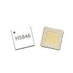
HMC5846LS6
v01.0414
Features
The HMC5846LS6 is ideal for:
Saturated Output Power: 35.5 dBm @ 30% PAE
• Point-to-Point Radios
High Output IP3: 42.5 dBm
• Point-to-Multi-Point Radios
High Gain: 31 dB
• VSAT & SATCOM
DC Supply: +7V @ 1200 mA
• Military & Space
No External Matching Required
TE
Typical Applications
General Description
Functional Diagram
LE
The HMC5846LS6 is a 4 stage GaAs pHEMT MMIC
2 Watt Power Amplifier with an integrated temperature
compensated power detector which operates between
12 and 16 GHz. The HMC5846LS6 provides 31 dB
of gain, 35.5 dBm of saturated output power, and
30% PAE from a +7V supply. The HMC5846LS6
exhibits excellent linearity and is optimized for high
capacity digital microwave radio. It is also ideal for
13.75 to 14.5 GHz Ku Band VSAT transmitters as well
as SATCOM applications.
B
SO
AMPLIFIERS - LINEAR & POWER - SMT
GaAs pHEMT MMIC 2 WATT POWER AMPLIFIER
WITH POWER DETECTOR, 12 - 16 GHz
Electrical Specifications, TA = +25 °C
O
Vdd = Vdd1, Vdd2, Vdd3, Vdd4, Vdd5 = +7V, Idd = 1200 mA [1]
Parameter
Min.
Frequency Range
Gain
26
Gain Variation Over Temperature
Input Return Loss
Output Return Loss
Output Power for 1 dB Compression (P1dB)
Typ.
12 - 16
32.5
Max.
Units
GHz
31
dB
0.06
dB/ °C
10
dB
17
dB
34.5
dBm
Saturated Output Power (Psat)
35.5
dBm
Output Third Order Intercept (IP3)[2]
42.5
dBm
Total Supply Current (Idd)
1200
mA
[1] Adjust Vgg between -2 to 0V to achieve Idd = 1200 mA typical.
[2] Measurement taken at +7V @ 1200 mA, Pout / Tone = +22 dBm
1
Information furnished by Analog Devices is believed to be accurate and reliable. However, no
For price, 2delivery,
and to
placeChelmsford,
orders: Analog MA
Devices,
Inc.,
For price,
delivery
and
to place
orders:
Microwave
Corporation,
Elizabeth
Drive,
01824
responsibility
is assumed
by Analog
Devices
for its use,
nor for anyHittite
infringements
of patents or other
One Technology Way, P.O. Box 9106, Norwood, MA 02062-9106
rights of third parties that may result from its use. Specifications subject to change without notice. No
Phone: 978-250-3343
Fax: 978-250-3373 Phone:
Order781-329-4700
On-line at www.hittite.com
• Order online at www.analog.com
license is granted by implication or otherwise under any patent or patent rights of Analog Devices.
Application
Support: Phone: 1-800-ANALOG-D
Trademarks and registered trademarks areApplication
the property of theirSupport:
respective owners.
Phone: 978-250-3343
or apps@hittite.com
�HMC5846LS6
v01.0414
GaAs pHEMT MMIC 2 WATT POWER AMPLIFIER
WITH POWER DETECTOR, 12 - 16 GHz
Broadband Gain &
Return Loss vs. Frequency
Gain vs. Temperature
40
30
GAIN (dB)
RESPONSE (dB)
34
20
10
0
30
26
-10
TE
22
-20
-30
18
10
11
12
13
14
15
FREQUENCY (GHz)
17
18
12
13
S11
S22
0
15
16
17
+25C
+85C
-40C
Output Return Loss vs. Temperature
0
-12
-16
-20
11
B
SO
-8
12
13
14
15
16
RETURN LOSS (dB)
-5
-4
-10
-15
-20
-25
-30
17
11
12
13
FREQUENCY (GHz)
+25C
+85C
14
15
16
17
FREQUENCY (GHz)
-40C
+25C
+85C
-40C
P1dB vs. Supply Voltage
O
P1dB vs. Temperature
38
38
36
36
34
34
P1dB (dBm)
P1dB (dBm)
14
FREQUENCY (GHz)
Input Return Loss vs. Temperature
RETURN LOSS (dB)
11
LE
S21
16
AMPLIFIERS - LINEAR & POWER - SMT
38
32
32
30
30
28
28
26
26
12
13
14
15
16
12
13
+25C
+85C
14
15
16
FREQUENCY (GHz)
FREQUENCY (GHz)
-40C
5V
6V
7V
Information furnished by Analog Devices is believed to be accurate and reliable. However, no
For price, 2delivery,
and to
placeChelmsford,
orders: Analog MA
Devices,
Inc.,
For price,
delivery
and
to place
orders:
Microwave
Corporation,
Elizabeth
Drive,
01824
responsibility
is assumed
by Analog
Devices
for its use,
nor for anyHittite
infringements
of patents or other
One Technology Way, P.O. Box 9106, Norwood, MA 02062-9106
rights of third parties that may result from its use. Specifications subject to change without notice. No
Phone: 978-250-3343
Fax: 978-250-3373 Phone:
Order781-329-4700
On-line at www.hittite.com
• Order online at www.analog.com
license is granted by implication or otherwise under any patent or patent rights of Analog Devices.
Application
Support: Phone: 1-800-ANALOG-D
Trademarks and registered trademarks areApplication
the property of theirSupport:
respective owners.
Phone: 978-250-3343
or apps@hittite.com
2
�HMC5846LS6
v01.0414
GaAs pHEMT MMIC 2 WATT POWER AMPLIFIER
WITH POWER DETECTOR, 12 - 16 GHz
38
36
36
Psat (dBm)
Psat (dBm)
Psat vs. Supply Voltage
38
34
32
30
34
32
TE
30
28
28
12
13
14
15
16
12
FREQUENCY (GHz)
13
+85C
5V
-40C
P1dB vs. Supply Current (Idd)
15
16
6V
7V
Psat vs. Supply Current (Idd)
38
38
36
36
32
28
26
12
13
14
15
Psat(dBm)
34
B
SO
34
30
32
30
28
26
16
12
13
FREQUENCY (GHz)
900mA
1000mA
O
46
44
44
42
42
IP3 (dBm)
48
1100mA
1200mA
40
38
36
36
34
34
32
32
30
16
Output IP3 vs.
Supply Current, Pout/Tone = +22 dBm
46
38
15
900mA
1000mA
48
40
14
FREQUENCY (GHz)
1100mA
1200mA
Output IP3 vs.
Temperature, Pout/Tone = +22 dBm
IP3 (dBm)
14
FREQUENCY (GHz)
LE
+25C
P1dB (dBm)
AMPLIFIERS - LINEAR & POWER - SMT
Psat vs. Temperature
30
12
13
14
15
16
12
13
FREQUENCY (GHz)
+25C
+85C
14
15
16
FREQUENCY (GHz)
-40C
900mA
1000mA
1100mA
1200mA
[1] Footnote if needed
3
Information furnished by Analog Devices is believed to be accurate and reliable. However, no
For price, 2delivery,
and to
placeChelmsford,
orders: Analog MA
Devices,
Inc.,
For price,
delivery
and
to place
orders:
Microwave
Corporation,
Elizabeth
Drive,
01824
responsibility
is assumed
by Analog
Devices
for its use,
nor for anyHittite
infringements
of patents or other
One Technology Way, P.O. Box 9106, Norwood, MA 02062-9106
rights of third parties that may result from its use. Specifications subject to change without notice. No
Phone: 978-250-3343
Fax: 978-250-3373 Phone:
Order781-329-4700
On-line at www.hittite.com
• Order online at www.analog.com
license is granted by implication or otherwise under any patent or patent rights of Analog Devices.
Application
Support: Phone: 1-800-ANALOG-D
Trademarks and registered trademarks areApplication
the property of theirSupport:
respective owners.
Phone: 978-250-3343
or apps@hittite.com
�HMC5846LS6
v01.0414
GaAs pHEMT MMIC 2 WATT POWER AMPLIFIER
WITH POWER DETECTOR, 12 - 16 GHz
Output IM3 @ Vdd = +5V
48
80
46
70
44
60
IM3 (dBc)
IP3 (dBm)
42
40
38
40
30
36
20
TE
34
10
32
30
0
12
13
14
15
16
10
FREQUENCY (GHz)
12
14
6V
7V
Output IM3 @ Vdd = +6V
18
20
22
24
12 GHz
13 GHz
14 GHz
15 GHz
16 GHz
Output IM3 @ Vdd = +7V
80
80
70
70
40
30
20
10
0
10
B
SO
50
12
14
16
18
20
22
IM3 (dBc)
60
60
50
40
30
20
10
0
10
24
12
14
12 GHz
13 GHz
14 GHz
15 GHz
O
Pout (dBm), GAIN (dB), PAE (%)
30
25
20
15
10
5
-6
-4
-2
0
Gain
24
14 GHz
15 GHz
16 GHz
2
4
6
8
35
30
25
20
15
10
5
0
-10
-8
-6
-4
INPUT POWER (dBm)
Pout
22
40
35
-8
20
Power Compression @ 14 GHz
40
0
-10
18
12 GHz
13 GHz
16 GHz
Power Compression @ 13 GHz
16
Pout/TONE (dBm)
Pout/TONE (dBm)
Pout (dBm), GAIN (dB), PAE (%)
16
Pout/TONE (dBm)
LE
5V
IM3 (dBc)
50
AMPLIFIERS - LINEAR & POWER - SMT
Output IP3 vs.
Supply Voltage, Pout/Tone = +22 dBm
-2
0
2
4
6
8
10
INPUT POWER (dBm)
PAE
Pout
Gain
PAE
Information furnished by Analog Devices is believed to be accurate and reliable. However, no
For price, 2delivery,
and to
placeChelmsford,
orders: Analog MA
Devices,
Inc.,
For price,
delivery
and
to place
orders:
Microwave
Corporation,
Elizabeth
Drive,
01824
responsibility
is assumed
by Analog
Devices
for its use,
nor for anyHittite
infringements
of patents or other
One Technology Way, P.O. Box 9106, Norwood, MA 02062-9106
rights of third parties that may result from its use. Specifications subject to change without notice. No
Phone: 978-250-3343
Fax: 978-250-3373 Phone:
Order781-329-4700
On-line at www.hittite.com
• Order online at www.analog.com
license is granted by implication or otherwise under any patent or patent rights of Analog Devices.
Application
Support: Phone: 1-800-ANALOG-D
Trademarks and registered trademarks areApplication
the property of theirSupport:
respective owners.
Phone: 978-250-3343
or apps@hittite.com
4
�HMC5846LS6
v01.0414
GaAs pHEMT MMIC 2 WATT POWER AMPLIFIER
WITH POWER DETECTOR, 12 - 16 GHz
Power Compression @ 15 GHz
Detector Voltage Over Temperature
10
30
Vref-Vdet (V)
25
20
15
0.1
10
5
0.01
-8
-6
-4
-2
0
2
4
6
8
10
3
11
Gain
27
12.5GHz +25C
12.5GHz +85C
12.5GHz -55C
PAE
Reverse Isolation vs. Temperature
35
15.5GHz +25C
15.5GHz +85C
15.5GHz -55C
Gain & Power vs.
Supply Current @ 14 GHz
-20
-30
-50
-60
-70
-80
-90
11
B
SO
-40
12
13
14
15
16
Gain (dB), P1dB (dBm), Psat (dBm)
40
0
-10
35
30
25
20
900
17
1000
+25C
+85C
1100
1200
Idd (mA)
FREQUENCY (GHz)
Gain
-40C
P1dB
Psat
O
Power Dissipation
45
10
9
POWER DISSIPATION (W)
Gain (dB), P1dB (dBm), Psat (dBm)
19
LE
Pout
-5
OUTPUT POWER (dBm)
INPUT POWER (dBm)
Gain & Power vs.
Supply Voltage @ 14 GHz
40
35
30
25
8
7
6
5
4
3
2
1
20
5
5.5
6
6.5
7
Vdd (V)
Gain
5
1
TE
Pout (dBm), GAIN (dB), PAE (%)
35
0
-10
ISOLATION (dB)
AMPLIFIERS - LINEAR & POWER - SMT
40
P1dB
0
-10
-8
-6
-4
-2
0
2
4
6
8
INPUT POWER (dBm)
Psat
Max Pdis @ 85C
12 GHz
13 GHz
14 GHz
15 GHz
16 GHz
Information furnished by Analog Devices is believed to be accurate and reliable. However, no
For price, 2delivery,
and to
placeChelmsford,
orders: Analog MA
Devices,
Inc.,
For price,
delivery
and
to place
orders:
Microwave
Corporation,
Elizabeth
Drive,
01824
responsibility
is assumed
by Analog
Devices
for its use,
nor for anyHittite
infringements
of patents or other
One Technology Way, P.O. Box 9106, Norwood, MA 02062-9106
rights of third parties that may result from its use. Specifications subject to change without notice. No
Phone: 978-250-3343
Fax: 978-250-3373 Phone:
Order781-329-4700
On-line at www.hittite.com
• Order online at www.analog.com
license is granted by implication or otherwise under any patent or patent rights of Analog Devices.
Application
Support: Phone: 1-800-ANALOG-D
Trademarks and registered trademarks areApplication
the property of theirSupport:
respective owners.
Phone: 978-250-3343
or apps@hittite.com
�HMC5846LS6
v01.0414
GaAs pHEMT MMIC 2 WATT POWER AMPLIFIER
WITH POWER DETECTOR, 12 - 16 GHz
Drain Bias Voltage (Vdd)
+8V
RF Input Power (RFIN)
+24 dBm
Channel Temperature
150 °C
150 °C
Nominal Junction Temperature
(T= 85 °C and Pin = 10 dBm)
90 °C
Continuous Pdiss (T= 85 °C)
(derate 133 mW/°C above 85 °C)
8.6 W
Operating Temperature
-55 to +85 °C
Thermal Resistance
(channel to ground paddle)
7.55 °C/W
Storage Temperature
-65 to +150 °C
Operating Temperature
-55 to +85 °C
ESD Sensitivity (HBM)
Class 1A Pass 250V
TE
Junction Temperature to Maintain
1 Million Hour MTTF
LE
ELECTROSTATIC SENSITIVE DEVICE
OBSERVE HANDLING PRECAUTIONS
O
B
SO
Outline Drawing
AMPLIFIERS - LINEAR & POWER - SMT
Reliability Information
Absolute Maximum Ratings
Package Information
Part Number
Package Body Material
Lead Finish
MSL Rating [2]
Package Marking [1]
HMC5846LS6
ALUMINA WHITE
Gold over Nickel
N/A
H5846
XXXX
[1] 4-Digit lot number XXXX
[2] Max peak reflow temperature of 260 °C
Information furnished by Analog Devices is believed to be accurate and reliable. However, no
For price, 2delivery,
and to
placeChelmsford,
orders: Analog MA
Devices,
Inc.,
For price,
delivery
and
to place
orders:
Microwave
Corporation,
Elizabeth
Drive,
01824
responsibility
is assumed
by Analog
Devices
for its use,
nor for anyHittite
infringements
of patents or other
One Technology Way, P.O. Box 9106, Norwood, MA 02062-9106
rights of third parties that may result from its use. Specifications subject to change without notice. No
Phone: 978-250-3343
Fax: 978-250-3373 Phone:
Order781-329-4700
On-line at www.hittite.com
• Order online at www.analog.com
license is granted by implication or otherwise under any patent or patent rights of Analog Devices.
Application
Support: Phone: 1-800-ANALOG-D
Trademarks and registered trademarks areApplication
the property of theirSupport:
respective owners.
Phone: 978-250-3343
or apps@hittite.com
6
�HMC5846LS6
v01.0414
GaAs pHEMT MMIC 2 WATT POWER AMPLIFIER
WITH POWER DETECTOR, 12 - 16 GHz
Function
Description
6
RFIN
This Pin is DC coupled and matched to 50 Ohms over the
operating frequency.
1-4
9, 10
Vdd4, Vdd3, Vdd2,
Vdd1, Vdd5, Vdd6
Drain bias voltage for the amplifier. External bypass capacitors of 100 pF are required for each pin followed by 0.01 μF
capacitors and a 4.7 μF capacitors.
8
Vgg1
Gate controlled amplifier. External bypass capacitors of
100 pF are required followed by 0.01 μF capacitors and a
4.7 μF capacitors.
5, 7, 13, 15,
16
GND
These Pins and Package bottom must be connected to
RF/DC ground.
11
Vref
DC voltage of diode biased through external resistor, used
for temperature compensation of Vdet.
12
Vdet
DC voltage representing RF output rectified by diode which
is biased through an external resistor.
LE
B
SO
14
Interface Schematic
TE
Pad Number
RFOUT
This Pin is DC coupled and matched to 50 Ohms.
Application Circuit
O
AMPLIFIERS - LINEAR & POWER - SMT
Pin Descriptions
7
Information furnished by Analog Devices is believed to be accurate and reliable. However, no
For price, 2delivery,
and to
placeChelmsford,
orders: Analog MA
Devices,
Inc.,
For price,
delivery
and
to place
orders:
Microwave
Corporation,
Elizabeth
Drive,
01824
responsibility
is assumed
by Analog
Devices
for its use,
nor for anyHittite
infringements
of patents or other
One Technology Way, P.O. Box 9106, Norwood, MA 02062-9106
rights of third parties that may result from its use. Specifications subject to change without notice. No
Phone: 978-250-3343
Fax: 978-250-3373 Phone:
Order781-329-4700
On-line at www.hittite.com
• Order online at www.analog.com
license is granted by implication or otherwise under any patent or patent rights of Analog Devices.
Application
Support: Phone: 1-800-ANALOG-D
Trademarks and registered trademarks areApplication
the property of theirSupport:
respective owners.
Phone: 978-250-3343
or apps@hittite.com
�HMC5846LS6
v01.0414
GaAs pHEMT MMIC 2 WATT POWER AMPLIFIER
WITH POWER DETECTOR, 12 - 16 GHz
O
List of Materials for Evaluation PCB EVAL01-HMC5846L56
Item
Description
J1, J2
PCB Mount K Connectors, SRI
J5, J6
DC Pins
C1 - C6, C20, C21, C23
100 pF Capacitors, 0402 Pkg.
C7 - C12, C19, C25, C26
0.01 μF Capacitors, 0603 Pkg.
C13 - C18, C29 - C31
4.7 μF Capacitors, Case A Pkg.
R1 - R2
40.2 kOhm Resistor, 0402 Pkg.
U1
HMC5846LS6 Amplifier
PCB [2]
128996 Evaluation PCB
[1] Reference this number when ordering complete evaluation PCB
AMPLIFIERS - LINEAR & POWER - SMT
B
SO
LE
TE
Evaluation PCB
[1]
The circuit board used in the application should use
RF circuit design techniques. Signal lines should
have 50 Ohm impedance while the package ground
leads and exposed paddle should be connected
directly to the ground plane similar to that shown.
A sufficient number of via holes should be used to
connect the top and bottom ground planes. The
evaluation board should be mounted to an appropriate heat sink. The evaluation circuit board shown
is available from Hittite upon request.
[2] Circuit Board Material: Rogers 4350
Information furnished by Analog Devices is believed to be accurate and reliable. However, no
For price, 2delivery,
and to
placeChelmsford,
orders: Analog MA
Devices,
Inc.,
For price,
delivery
and
to place
orders:
Microwave
Corporation,
Elizabeth
Drive,
01824
responsibility
is assumed
by Analog
Devices
for its use,
nor for anyHittite
infringements
of patents or other
One Technology Way, P.O. Box 9106, Norwood, MA 02062-9106
rights of third parties that may result from its use. Specifications subject to change without notice. No
Phone: 978-250-3343
Fax: 978-250-3373 Phone:
Order781-329-4700
On-line at www.hittite.com
• Order online at www.analog.com
license is granted by implication or otherwise under any patent or patent rights of Analog Devices.
Application
Support: Phone: 1-800-ANALOG-D
Trademarks and registered trademarks areApplication
the property of theirSupport:
respective owners.
Phone: 978-250-3343
or apps@hittite.com
8
�