HMC625LP5 / 625LP5E
v09.0410
0.5 dB LSB GaAs MMIC 6-BIT DIGITAL
VARIABLE GAIN AMPLIFIER, DC - 6 GHz
Typical Applications
Features
The HMC625LP5(E) is ideal for:
-13.5 to +18 Gain Control in 0.5 dB Steps
• Cellular/3G Infrastructure
Power-up State Selection
• WiBro / WiMAX / 4G
High Output IP3: +33 dBm
• Microwave Radio & VSAT
TTL/CMOS Compatible
Serial, Parallel, or latched Parallel Control
• Test Equipment and Sensors
• IF & RF Applications
±0.25 dB Typical Gain Step Error
Single +5V Supply
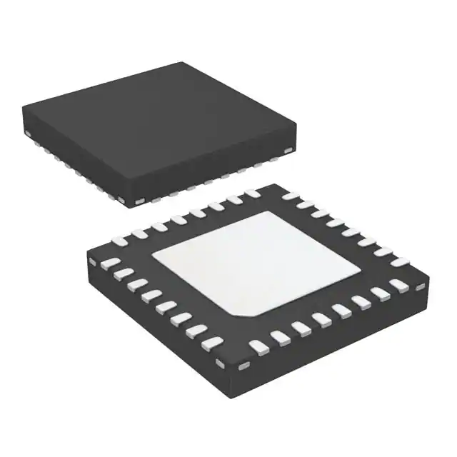
32 Lead 5x5mm SMT Package: 25mm2
VARIABLE GAIN AMPLIFIERS - DIGITAL - SMT
12
12 - 1
Functional Diagram
General Description
The HMC625LP5(E) is a digitally controlled variable
gain amplifier which operates from DC to 6 GHz, and
can be programmed to provide anywhere from 13.5
dB attenuation, to 18 dB of gain, in 0.5 dB steps. The
HMC625LP5(E) delivers noise figure of 6 dB in its
maximum gain state, with output IP3 of up to +33 dBm
in any state. The dual mode control interface is CMOS/
TTL compatible, and accepts either a three wire serial
input or a 6 bit parallel word. The HMC625LP5(E) also
features a user selectable power up state and a serial
output port for cascading other Hittite serial controlled
components. The HMC625LP5(E) is housed in a
RoHS compliant 5x5 mm QFN leadless package, and
requires no external matching components.
Electrical Specifi cations, TA = +25° C, 50 Ohm System, Vdd= +5V, Vs= +5V
Parameter
Gain (Maximum Gain State)
Frequency
Min.
Typ.
DC - 3.0 GHz
3.0 - 6.0 GHz
13
5
18
13
dB
dB
31.5
dB
15
dB
Gain Control Range
Input Return Loss
DC - 6.0 GHz
Max.
Units
Output Return Loss
DC - 6.0 GHz
12
dB
Gain Accuracy: (Referenced to Maximum Gain State)
All Gain States
DC - 0.8 GHz
0.8 - 6.0 GHz
± (0.10 + 5% of Gain Setting) Max.
± (0.30 + 3% of Gain Setting) Max.
dB
dB
Output Power for 1dB Compression
DC - 3.0 GHz
3.0 - 6.0 GHz
Output Third Order Intercept Point
(Two-Tone Input Power= 0 dBm Each Tone)
16
13
19
16
dBm
DC - 6.0 GHz
33
dBm
Noise Figure
DC - 6.0 GHz
6
dB
Supply Current (Idd)
DC - 6.0 GHz
60
88
100
mA
For price, delivery and to place orders: Hittite Microwave Corporation, 20 Alpha Road, Chelmsford, MA 01824
Phone: 978-250-3343
Fax: 978-250-3373
Order On-line at www.hittite.com
Application Support: Phone: 978-250-3343 or apps@hittite.com
�HMC625LP5 / 625LP5E
v09.0410
0.5 dB LSB GaAs MMIC 6-BIT DIGITAL
VARIABLE GAIN AMPLIFIER, DC - 6 GHz
Normalized Attenuation [2]
(Only Major States are Shown)
Maximum Gain vs. Frequency
25
0
NORMALIZED ATTENUATION (dB)
[1]
20
15
[2]
5
0
-5
-10
+25 C
+85 C
-40 C
-15
-20
-25
-10
-15
-20
-25
-30
-35
0
1
2
3
4
5
6
0
0.5
1
FREQUENCY (GHz)
1.5
2
2.5
3
3.5
Input Return Loss [1]
Output Return Loss [1]
(Only Major States are Shown)
(Only Major States are Shown)
4.5
5
5.5
6
12
0
-5
-5
-10
-10
RETURN LOSS (dB)
RETURN LOSS (dB)
0
-15
-20
-25
-30
-35
-15
-20
-25
-30
-35
-40
-40
0
1
2
3
4
5
6
0
1
FREQUENCY (GHz)
2
3
4
5
6
5
6
FREQUENCY (GHz)
Input Return Loss [2]
Output Return Loss [2]
(Only Major States are Shown)
(Only Major States are Shown)
0
0
-5
-5
-10
-10
RETURN LOSS (dB)
RETURN LOSS (dB)
4
FREQUENCY (GHz)
-15
-20
-25
-30
-35
-15
-20
-25
-30
-35
-40
-40
0
1
2
3
4
5
6
FREQUENCY (GHz)
0
1
2
3
4
FREQUENCY (GHz)
[1] Tested with broadband bias tee on RF ports and C1 = 10,000pF
[2] C1, C6 and C8 = 100pF, L1 = 24nH
For price, delivery and to place orders: Hittite Microwave Corporation, 20 Alpha Road, Chelmsford, MA 01824
Phone: 978-250-3343
Fax: 978-250-3373
Order On-line at www.hittite.com
Application Support: Phone: 978-250-3343 or apps@hittite.com
VARIABLE GAIN AMPLIFIERS - DIGITAL - SMT
GAIN (dB)
10
-5
12 - 2
�HMC625LP5 / 625LP5E
v09.0410
0.5 dB LSB GaAs MMIC 6-BIT DIGITAL
VARIABLE GAIN AMPLIFIER, DC - 6 GHz
Bit Error vs. Frequency [2]
Bit Error vs. Attenuation State [2]
(Only Major States are Shown)
2
1
1.5
0.8
0.6
500MHz, 1GHz, 2GHz
BIT ERROR (dB)
BIT ERROR (dB)
1
0.5
0
-0.5
0.4
0.2
0
-0.2
-0.4
-1
100MHz, 3GHz, 4GHz
-0.6
-1.5
-0.8
-2
-1
0
1
4
5
6
0
4
8
12
16
20
24
28
32
ATTENUATION STATE (dB)
Normal Relative Phase vs. Frequency [2]
Step Error vs. Frequency [2]
(Only Major States are Shown)
(Only Major States are Shown)
80
1
0.8
31.5 dB
60
0.6
16 dB
STEP ERROR (dB)
RELATIVE PHASE (deg)
VARIABLE GAIN AMPLIFIERS - DIGITAL - SMT
3
FREQUENCY (GHz)
12
12 - 3
2
40
8 dB
20
0
0.5 - 4 dB
-20
0.4
0.2
0
-0.2
-0.4
-0.6
-0.8
-40
-1
0
1
2
3
4
5
6
FREQUENCY (GHz)
0
1
2
3
4
5
6
FREQUENCY (GHz)
[1] Tested with broadband bias tee on RF ports and C1 = 10,000pF
[2] C1, C6 and C8 = 100pF, L1 = 24nF
For price, delivery and to place orders: Hittite Microwave Corporation, 20 Alpha Road, Chelmsford, MA 01824
Phone: 978-250-3343
Fax: 978-250-3373
Order On-line at www.hittite.com
Application Support: Phone: 978-250-3343 or apps@hittite.com
�HMC625LP5 / 625LP5E
v09.0410
0.5 dB LSB GaAs MMIC 6-BIT DIGITAL
VARIABLE GAIN AMPLIFIER, DC - 6 GHz
Serial Control Interface
The HMC625LP5(E) contains a 3-wire SPI compatible digital interface (SERIN, CLK, LE). It is activated when P/S
is kept high. The 6-bit serial word must be loaded MSB first. The positive-edge sensitive CLK and LE requires
clean transitions. If mechanical switches were used, sufficient debouncing should be provided. When LE is high,
6-bit data in the serial input register is transferred to the attenuator. When LE is high CLK is masked to prevent data
transition during output loading.
When P/S is low, 3-wire SPI interface inputs (SERIN, CLK, LE) are disabled and serial input register is loaded
asynchronously with parallel digital inputs (D0-D5). When LE is high, 6-bit parallel data is transferred to the attenuator.
For all modes of operations, the DVGA state will stay constant while LE is kept low.
Parameter
Typ.
Min. serial period, tSCK
100 ns
Control set-up time, tCS
20 ns
Control hold-time, tCH
20 ns
LE setup-time, tLN
10 ns
Min. LE pulse width, tLEW
10 ns
Min LE pulse spacing, tLES
630 ns
Serial clock hold-time from LE, tCKN
10 ns
Hold Time tPH
0 ns
Latch Enable Minimum width, tLEN
10 ns
Setup Time, tPS
2 ns
Timing Diagram (Latched Parallel Mode)
Parallel Mode (Direct Parallel Mode & Latched Parallel Mode)
Note: The parallel mode is enabled when P/S is set to low.
Direct Parallel Mode - The attenuation state is changed by the Control Voltage Inputs directly. The LE (Latch Enable)
must be at a logic high to control the attenuator in this manner.
Latched Parallel Mode - The attenuation state is selected using the Control Voltage Inputs and set while the LE is in
the Low state. The attenuator will not change state while LE is Low. Once all Control Voltage Inputs are at the desired
states the LE is pulsed. See timing diagram above for reference.
For price, delivery and to place orders: Hittite Microwave Corporation, 20 Alpha Road, Chelmsford, MA 01824
Phone: 978-250-3343
Fax: 978-250-3373
Order On-line at www.hittite.com
Application Support: Phone: 978-250-3343 or apps@hittite.com
VARIABLE GAIN AMPLIFIERS - DIGITAL - SMT
12
12 - 4
�HMC625LP5 / 625LP5E
v09.0410
0.5 dB LSB GaAs MMIC 6-BIT DIGITAL
VARIABLE GAIN AMPLIFIER, DC - 6 GHz
PUP Truth Table
Power-Up States
If LE is set to logic LOW at power-up, the logic state of
PUP1 and PUP2 determines the power-up state of the
part per PUP truth table. If the LE is set to logic HIGH
at power-up, the logic state of D0-D5 determines the
power-up state of the part per truth table. The DVGA
latches in the desired power-up state approximately
200 ms after power-up.
Power-On Sequence
VARIABLE GAIN AMPLIFIERS - DIGITAL - SMT
12
12 - 5
The ideal power-up sequence is: GND, Vdd, digital
inputs, RF inputs. The relative order of the digital
inputs are not important as long as they are powered
after Vdd / GND
RF Input Power [1]
11.5 dBm (T = 85 °C)
Digital Inputs (Reset, Shift Clock,
Latch Enable & Serial Input)
-0.5 to Vdd +0.5V
5.6V
Collector Bias Voltage (Vcc)
5.5V
Channel Temperature
150 °C
Continuous Pdiss (T = 85 °C)
(derate 15.1 mW/°C above 85 °C) [1]
0.98 W
Thermal Resistance
66.3 °C/W
Storage Temperature
-65 to +150 °C
Operating Temperature
PUP1
PUP2
Gain Relative to Maximum
Gain
0
0
0
-31.5
0
1
0
-24
0
0
1
-16
0
1
1
Insertion Loss
1
X
X
0 to -31.5 dB
Note: The logic state of D0 - D5 determines the
power-up state per truth table shown below when LE
is high at power-up.
Truth Table
Absolute Maximum Ratings
Bias Voltage (Vdd)
LE
-40 to +85 °C
[1] At max gain settling
Control Voltage Input
Gain
Relative to
Maximum
Gain
D5
D4
D3
D2
D1
D0
High
High
High
High
High
High
0 dB
High
High
High
High
High
Low
-0.5 dB
High
High
High
High
Low
High
-1 dB
High
High
High
Low
High
High
-2 dB
High
High
Low
High
High
High
-4 dB
High
Low
High
High
High
High
-8 dB
Low
High
High
High
High
High
-16 dB
Low
Low
Low
Low
Low
Low
-31.5 dB
Any combination of the above states will provide a reduction in
gain approximately equal to the sum of the bits selected.
Control Voltage Table
Bias Voltage
Vdd (V)
Idd (Typ.) (mA)
State
Vdd = +3V
Vdd = +5V
5V
2
Low
0 to 0.5V @