HMC701LP6CE
v09.1112
8 GHz 16-BIT FRACTIONAL-N PLL
PLL - Fractional-N - SMT
Features
1
• Fractional or Integer Modes
• Low Fractional Spurious
• 8 GHz, 16-Bit RF N-Counter
• Reference spurs: -90 dBc typ
• 24-Bit Step Size Resolution, 3 Hz typ
• Auto and Triggered Sweeper Functions
• Ultra Low Phase Noise 6 GHz, 50 MHz Ref.
-103 / -110 dBc/Hz @ 20 kHz (Frac / Integer)
• Cycle Slip Prevention (CSP) for fast settling
• Auxiliary Clock Source
• Reference Path Input: 200 MHz
• 40 Lead 6x6 mm SMT Package: 36 mm²
• 14-Bit Reference Path Divider
Typical Applications
• Base Stations for Mobile Radio
(GSM, PCS, DCS, CDMA, WCDMA)
• CATV Equipment
• Wireless LANs, WiMax
• Automotive Radar
• Communications Test Equipment
• Phased-Array Systems
• FMCW Sensors
Functional Diagram
Information furnished by Analog Devices is believed to be accurate and reliable. However, no
For price, 20
delivery,
and
to place
orders: Analog
For price,
delivery
and
to place
orders:
Microwave
Corporation,
Alpha
Road,
Chelmsford,
MADevices,
01824 Inc.,
responsibility
is assumed
by Analog
Devices
for its use,
nor for anyHittite
infringements
of patents or other
One Technology Way, P.O. Box 9106, Norwood, MA 02062-9106
rights of third parties that may result from its use. Specifications subject to change without notice. No
Phone: 978-250-3343
Fax: 978-250-3373
Order
at www.hittite.com
Phone: On-line
781-329-4700
• Order online at www.analog.com
license is granted by implication or otherwise under any patent or patent rights of Analog Devices.
Application
Support: Phone: 1-800-ANALOG-D
Trademarks and registered trademarks are
the property of their
respective owners.
Application
Support:
Phone: 978-250-3343
or apps@hittite.com
�HMC701LP6CE
v09.1112
8 GHz 16-BIT FRACTIONAL-N PLL
The HMC701LP6CE is a SiGe BiCMOS fractional-N PLL. The PLL includes a 8GHz 16-bit RF N-Divider, a 24-bit deltasigma modulator, a very low noise digital phase frequency detector (PFD), and a precision controlled charge pump.
The fractional-N PLL features an advanced delta-sigma modulator design that allows ultra-fine frequency step sizes.
The fractional-N PLL features the ability to alter both the phase-frequency detector (PFD) gain and the cycle slipping
characteristics of the PFD. This feature can reduce the time to arrive at the new frequency by 50% vs. conventional
PFDs. Ultra low in-close phase noise also allows wider loop bandwidths for faster frequency hopping.
The fractional-N PLL contains a built-in linear sweeper function, which allows it to perform frequency chirps with a
wide variety of sweep times, polarities and dwells, all with an external or automatic sweep trigger.
In addition the fractional-N PLL has a number of auxiliary clock generation modes that can be accessed via the GPO.
Electrical Specifications, TA = +25°C
PLL - Fractional-N - SMT
General Description
VCCHF = VCCPRS = RVDD = +3.3V
VPPCP = VCCOA = VDDPDR = VPPDRV = VDDPD = VDDPDV = +5V
DVDD = DVDDIO = DVDDQ = +3.3V
GNDDRV = GNDCP = GNDPD = GNDPDV = GNDPDR = 0V
Table 1. Electrical Specifications
Parameter
Conditions / Notes
Min
Typ
Max RF Input Frequency (3.3V)
8
9
Max RF Input Frequency (2.7 - 3.3V)
7
8
Max
Units
Prescaler Characteristics
GHz
GHz
Min RF Input Frequency
0.1
RF Input Power
-10
16-bit N-Divider Range (Integer)
32
65,535
35
65,531
16-bit N-Divider Range (Fractional)
Fraction Nominal Divide ratio varies
(-3 / +4) dynamically max
MHz
-6
10
dBm
REF Input Characteristics
Max Ref Input Frequency (pin XREFP)
250
200
MHz
Max Ref Input Frequency (pin XSIN)
250
220
MHz
Min Ref Input Frequency
Ref Input Voltage Range (pin XREFP)
Ref Input Power Range (pin XSIN)
50 Ω Source. XSIN minimum
20MHz due to phase noise degradation
100
AC Coupled
750
1000
3300
mVpp
-6
0
12
dBm
5
pF
Ref Input Capacitance
14-Bit R-Divider Range
1
kHz
16,383
Information furnished by Analog Devices is believed to be accurate and reliable. However, no
For price, 20
delivery,
and
to place
orders: Analog
For price,
delivery
and
to place
orders:
Microwave
Corporation,
Alpha
Road,
Chelmsford,
MADevices,
01824 Inc.,
responsibility
is assumed
by Analog
Devices
for its use,
nor for anyHittite
infringements
of patents or other
One Technology Way, P.O. Box 9106, Norwood, MA 02062-9106
rights of third parties that may result from its use. Specifications subject to change without notice. No
Phone: 978-250-3343
Fax: 978-250-3373
Order
at www.hittite.com
Phone: On-line
781-329-4700
• Order online at www.analog.com
license is granted by implication or otherwise under any patent or patent rights of Analog Devices.
Application
Support: Phone: 1-800-ANALOG-D
Trademarks and registered trademarks are
the property of their
respective owners.
Application
Support:
Phone: 978-250-3343
or apps@hittite.com
2
�HMC701LP6CE
v09.1112
8 GHz 16-BIT FRACTIONAL-N PLL
Table 1. Electrical Specifications
(Continued)
PLL - Fractional-N - SMT
Parameter
Conditions / Notes
Min
Typ
Max
Units
0.1
70
MHz
0.1
100
MHz
Phase Detector
Fractional Mode
Phase Detector Frequency
Integer Mode
Phase Detector Frequency
Charge Pump
Max Output Current
4
mA
Min Output Current
125
µA
Charge Pump Gain Step Size (5-bits)
125
µA
Charge Pump Trim Step Size (3-bits)
14
µA
Charge Pump Offset Step Size (4-bits)
29
µA
PFD / Charge Pump Noise (Integer)
6 GHz, 50 MHz Ref, Input referred
1 kHz
-141
dBc/Hz
10 kHz
-149
dBc/Hz
100 kHz
-155
dBc/Hz
Less than 3 dB degradation typ. at
these limits
Compliance Voltage
-406 µA Offset
0.4
VPPCP-0.8
V
-406 µA Offset
0.8
VPPCP-0.4
V
Logic Inputs
VIH Input High Voltage
V
VDDIO-0.4
VIL Input Low Voltage
0.4
V
0.1
V
Logic Outputs
VIH Output High Voltage
V
VDDIO-0.1
VIL Output Low Voltage
Power Supply Voltages
VCC - Analog 3V Supplies
VCCPRS, RVDD, VCCHF
3
3.3
3.45
V
DVDD, DVDDQ
3
3.3
3.45
V
DVDDIO
3
3.3
3.45
V
VCCOA, VPPCP, VPPDRV,
VDDPD, VDDPDV, VDDPDR
4.5
5.0
5.5
V
DVDD - Digital Internal Supply
DVDDIO - Digital I/o Supply
Analog 5V Supplies
Power Supply Current (6 GHz Fractional Mode, 50 MHz PFD)
VCCOA, VPPCP, VPPDRV,
VDDPD, VDDPDV, VDDPDR
37
mA
Analog +3.3V
VCCPRS, RVDD, VCCHF
71
mA
Digital +3.3V
DVDD, DVDDIO, DVDDQ
19
mA
Reg 01h = 0
Crystal not clocked
6
µA
Reg 01h = 0
Crystal clocked 100 MHz
20
Analog +5V
Power Down - Crystal Off
Power Down - Crystal On, 100 MHz
3
200
µA
Information furnished by Analog Devices is believed to be accurate and reliable. However, no
For price, 20
delivery,
and
to place
orders: Analog
For price,
delivery
and
to place
orders:
Microwave
Corporation,
Alpha
Road,
Chelmsford,
MADevices,
01824 Inc.,
responsibility
is assumed
by Analog
Devices
for its use,
nor for anyHittite
infringements
of patents or other
One Technology Way, P.O. Box 9106, Norwood, MA 02062-9106
rights of third parties that may result from its use. Specifications subject to change without notice. No
Phone: 978-250-3343
Fax: 978-250-3373
Order
at www.hittite.com
Phone: On-line
781-329-4700
• Order online at www.analog.com
license is granted by implication or otherwise under any patent or patent rights of Analog Devices.
Application
Support: Phone: 1-800-ANALOG-D
Trademarks and registered trademarks are
the property of their
respective owners.
Application
Support:
Phone: 978-250-3343
or apps@hittite.com
�HMC701LP6CE
v09.1112
8 GHz 16-BIT FRACTIONAL-N PLL
(Continued)
Parameter
Conditions / Notes
Min
Typ
Max
Units
Temperature Sensor (3-bit)
Min Temperature
Readout: 000
-32
Max Temperature
Readout: 111
+82
°C
Temp Change / LSB
17.5
°C/LSB
Worst Case Absolute Temp Error
±10
°C
2
mA
700
mV
Current Consumption (when Enabled)
°C
Power on Reset All digital inputs must be Tref to reset. Recommended after power-up.
22
DVDD
Supply
Digital Power Supply, Nominally +3.3V
23
GPO1
DO
General Purpose Output 1 with Tristate
24
GPO2
DO
General Purpose Output 2 with Tristate
25
GPO3
DIO
General Purpose Input/Output with Tristate
may be configured for External Ramp trigger Input. See register REG 14h[5]
27
SEN
CMOS I/P
Main Serial port enable input
28
SDI
CMOS I/P
Main Serial port data input
Main Serial port clock input
Square Wave Crystal Ref Input
Power Supply for Ref Path, Nominally +3.3V
Sinusoidal Crystal reference input
29
SCK
CMOS I/P
30
VSLE
DO
Leave pin disconnected.
31
VSDO
DO
Leave pin disconnected.
32
VSCK
DO
33
LD_SDO
CMOS O/P
Leave pin disconnected.
34
DVDDIO
Supply
Power Supply for digital I/O, matches external Digital Supply in 1.8V to 5.5V range
35
DVDD
Supply
Internal Digital Power Supply. Nominally 3.3V
36
DVDDQ
Supply
Power Supply Isolation pin. Nominally 3.3V, bypassed to GND, zero current.
37
VCOIP
RF I/P
Complementary Input to the RF Prescaler. If single ended input, this point must be
decoupled to the ground plane with a ceramic bypass capacitor, typically 100 pF
38
VCOIN
RF I/P
Input to the RF Prescaler. This signal input is ac-coupled to the external VCO
39
VCCHF
Supply
RF Section Power Supply. Nominally 3.3V
40
BIAS
Analog I/P
Lock Detect or Main Serial Port Data Output
Decoupling Pin for RF section, nominally external 1nF bypassed to VCCHF
Information furnished by Analog Devices is believed to be accurate and reliable. However, no
For price, 20
delivery,
and
to place
orders: Analog
For price,
delivery
and
to place
orders:
Microwave
Corporation,
Alpha
Road,
Chelmsford,
MADevices,
01824 Inc.,
responsibility
is assumed
by Analog
Devices
for its use,
nor for anyHittite
infringements
of patents or other
One Technology Way, P.O. Box 9106, Norwood, MA 02062-9106
rights of third parties that may result from its use. Specifications subject to change without notice. No
Phone: 978-250-3343
Fax: 978-250-3373
Order
at www.hittite.com
Phone: On-line
781-329-4700
• Order online at www.analog.com
license is granted by implication or otherwise under any patent or patent rights of Analog Devices.
Application
Support: Phone: 1-800-ANALOG-D
Trademarks and registered trademarks are
the property of their
respective owners.
Application
Support:
Phone: 978-250-3343
or apps@hittite.com
�HMC701LP6CE
v09.1112
8 GHz 16-BIT FRACTIONAL-N PLL
Typical Phase Noise - Fractional Mode
-90
-90
6 GHz Integer
-100
PHASE NOISE (dBc/Hz)
PHASE NOISE (dBc/Hz)
-110
1 GHz Integer
-120
-130
-140
All Plots 50 MHz PFD
-150
6 GHz Fractional
-100
2 GHz Integer
-160
2 GHz Fractional
-110
-120
-130
All Plots 50 MHz PFD
-140
-150
-160
-170
1000
10
4
10
5
10
6
10
7
10
-170
1000
8
4
5
10
RF Divider Sensitivity
6
7
10
10
FREQUENCY (Hz)
FREQUENCY (Hz)
8
10
10
Frequency Sweep
6150
20
+85C
FRAC
INTEG
6100
+25C
0
FREQUENCY (MHz)
INPUT POWER (dBm)
10
-40C
-10
-20
6000
5950
5900
-30
-40
6050
PLL - Fractional-N - SMT
Typical Phase Noise - Integer Mode
0
2000
4000
6000
FREQUENCY (MHz)
8000
5850
-2
10000
-1
0
1
2
3
TIME (ms)
Cycle Slip Prevention: Frequency Hop
from 5200 MHz to 3950 MHz
5300
FREQUENCY (MHz)
5100
4900
CSP OFF
4700
4500
CSP ON
4300
4100
3900
-10
0
10
20
30
40
50
60
70
TIME (μs)
Information furnished by Analog Devices is believed to be accurate and reliable. However, no
For price, 20
delivery,
and
to place
orders: Analog
For price,
delivery
and
to place
orders:
Microwave
Corporation,
Alpha
Road,
Chelmsford,
MADevices,
01824 Inc.,
responsibility
is assumed
by Analog
Devices
for its use,
nor for anyHittite
infringements
of patents or other
One Technology Way, P.O. Box 9106, Norwood, MA 02062-9106
rights of third parties that may result from its use. Specifications subject to change without notice. No
Phone: 978-250-3343
Fax: 978-250-3373
Order
at www.hittite.com
Phone: On-line
781-329-4700
• Order online at www.analog.com
license is granted by implication or otherwise under any patent or patent rights of Analog Devices.
Application
Support: Phone: 1-800-ANALOG-D
Trademarks and registered trademarks are
the property of their
respective owners.
Application
Support:
Phone: 978-250-3343
or apps@hittite.com
6
�HMC701LP6CE
v09.1112
8 GHz 16-BIT FRACTIONAL-N PLL
Theory of Operation
PLL - Fractional-N - SMT
The HMC701LP6CE synthesizer consists of the following functional blocks
1. Reference Path Input Buffers
2. Reference Path Divider
3. VCO Path Input Buffer
4. VCO Path Multi-Modulus Prescaler/Divider
5. Δ∑ Fractional Modulator
6. Phase Frequency Detector
7. Charge Pump
8. Main Serial Port
9. Auxiliary Serial Port
10. Temperature Sensor
11. Power On Reset Circuit
12. CW Sweeper Subsystem
13. Auxiliary Clock Generator
14. General Purpose Output (GPO) Bus
15. Multiple VCO Controller
Each of these blocks is described briefly in the following section.
Reference Path
The full Reference Path block diagram is shown in Figure 1 The ultra low noise phase detector requires the best
possible reference signal. Since a given application may desire to use a square wave or a 50 Ohm sinusoidal crystal
source, HMC701LP6CE offers two input ports, each one optimized for the lowest possible noise for the source type
being used.
For absolute best low noise performance, the sine wave path should be used.
The user should use only one Ref path input, that is the input that matches their reference source type. Note the input
is defaulted to the square wave input on power up. Should the sine reference path be used, it is necessary to enable
the sine input, shut down the square wave input and set the mux (rfp_buf_sin_en=1, rfp_buf_sq_en=0, rfp_buf_sin_
sel=1, Table 12). The unused port should be left open.
The reference path supports input frequencies of up to 250 MHz typical, however the maximum frequency at the
phase detector (PFD) depends upon the mode of operation, worst case at +85°C, 70 MHz in fractional mode and
100 MHz in integer mode. Hence reference inputs of greater than the PFD maximum frequency must use the
appropriate R divider setting.
Figure 1. Reference Sine Input Stages
The unused reference port is normally not connected.
7
Information furnished by Analog Devices is believed to be accurate and reliable. However, no
For price, 20
delivery,
and
to place
orders: Analog
For price,
delivery
and
to place
orders:
Microwave
Corporation,
Alpha
Road,
Chelmsford,
MADevices,
01824 Inc.,
responsibility
is assumed
by Analog
Devices
for its use,
nor for anyHittite
infringements
of patents or other
One Technology Way, P.O. Box 9106, Norwood, MA 02062-9106
rights of third parties that may result from its use. Specifications subject to change without notice. No
Phone: 978-250-3343
Fax: 978-250-3373
Order
at www.hittite.com
Phone: On-line
781-329-4700
• Order online at www.analog.com
license is granted by implication or otherwise under any patent or patent rights of Analog Devices.
Application
Support: Phone: 1-800-ANALOG-D
Trademarks and registered trademarks are
the property of their
respective owners.
Application
Support:
Phone: 978-250-3343
or apps@hittite.com
�HMC701LP6CE
v09.1112
8 GHz 16-BIT FRACTIONAL-N PLL
The crystal reference sine input stage is shown in Figure 2. This is the lowest noise reference path. This is a common
emitter single ended bipolar buffer. The XSIN input pin is DC coupled and has about 950 mV bias on it. Expected
input is a 0 dBm sinusoid from a 50 Ohm source. Normally the input should be AC coupled externally. The sine buffer
input impedance is dominated by a 25 Ohm shunt resistor in series with a 50 pF on chip cap. Should a lower input
impedance be needed, an external 50 Ohm shunt resistor can be used, DC isolated by an external bypass cap. The
sine input reference path phase noise floor is approximately equivalent to -159 dBc/Hz. For best performance care
should be taken to provide a crystal reference source with equivalent or better phase noise floor.
PLL - Fractional-N - SMT
Sine Reference Input
Figure 2. Ref Sine Input
Square Wave Reference Input
The square wave Ref Input stage is shown in Figure 3. The stage is designed to accept square wave inputs from CML
to CMOS levels. Slightly degraded phase noise performance may be obtained with quasi sine 1 Vpp inputs. It may be
necessary to attenuate very large CMOS levels if absolute best in close phase noise performance is required. Input
reference should have a noise floor better than -160 dBc/Hz to avoid degradation of the input reference path.
Figure 3. Square Wave Ref Input Stage
Information furnished by Analog Devices is believed to be accurate and reliable. However, no
For price, 20
delivery,
and
to place
orders: Analog
For price,
delivery
and
to place
orders:
Microwave
Corporation,
Alpha
Road,
Chelmsford,
MADevices,
01824 Inc.,
responsibility
is assumed
by Analog
Devices
for its use,
nor for anyHittite
infringements
of patents or other
One Technology Way, P.O. Box 9106, Norwood, MA 02062-9106
rights of third parties that may result from its use. Specifications subject to change without notice. No
Phone: 978-250-3343
Fax: 978-250-3373
Order
at www.hittite.com
Phone: On-line
781-329-4700
• Order online at www.analog.com
license is granted by implication or otherwise under any patent or patent rights of Analog Devices.
Application
Support: Phone: 1-800-ANALOG-D
Trademarks and registered trademarks are
the property of their
respective owners.
Application
Support:
Phone: 978-250-3343
or apps@hittite.com
8
�HMC701LP6CE
v09.1112
8 GHz 16-BIT FRACTIONAL-N PLL
PLL - Fractional-N - SMT
Reference Path ’R’ Divider
The referenced path features a 14-bit divider (rfp_div_ratio, Reg03h Table 14) and can divide input signals
at up to 250 MHz by numbers from 1 to 16,383. The selected input reference source may be divided or bypassed
(rfp_div_select), and applied to the phase detector reference input.
Reference Path Test Features
A fractional synthesizer is a complex combination of a low phase noise analog oscillator running in close proximity with
a nearly randomly modulated delta-sigma digital modulator.
Clean spur free operation of the synthesizer requires proper board layout of power and grounds. Spurious sources
are often difficult to identify and may be related to harmonics of the digital modulation which land near the operating
frequency of the VCO, or they may arise from repeating patterns in the digital modulation itself . The loop filter and the
fractional modulator are designed to suppress these fractional spurs, but it is sometimes the case that the isolation
of the spurious products comes from layout issues. The problem is how to identify the sources of spurious products
if they occur?
The reference path of the HMC701LP6CE features some interesting test options for clocking the digital portion of the
synthesizer which may provide for a better understanding of the source of reference spurs should they occur. See
Figure 4, Table 12 and Table 29 for more register details.
For normal operation, Reg3h[15]=1. When Reg3h[15]=1, (rfp_auto_refdiv select enabled) then Reg 3 [14] & Reg 1 [2]
are ignored. If Reg 3 [13:0] is programmed to >=2, RefDiv will be enabled and the divided output will be fed to the PFD.
If Reg 3 [13:0] is programmed to 1, RefDiv will be disabled and the undivided reference signal will be fed to the PFD.
When Reg3h[15]=0 (rfp_auto_refdiv select disabled), then the state of the RefDiv is controlled by Reg 3 [14] & Reg
1 [2]. Then to enable RefDiv Reg 1 [2] = 1. To pass the divided reference signal to the PFD, Reg 3 [14]=1. If Reg
3 [14]=0, the undivided reference is passed directly to the PFD. This configuration would typically only be used for
engineering test. It allows the RefDiv to be running while the PFD is operating with the undivided reference. This
allows inspection for spurs that may be manifest from the divider running.
It is possible for example to set the synthesizer to integer mode of operation, where the digital harmonics normally
fall directly on the VCO frequency. We might chose for example to use the sine source (rfp_buf_sine_sel=1, div_
todig_en=0) to drive the reference divider. In such a case the delta sigma modulator is not normally used, however if
we wish to test the effects of the digital power supply isolation, we could input a 2nd reference source on the square
wave input, enable its buffer (rfp_buf_sq_en=1), and enable the 2nd crystal to clock the unused delta sigma modulator
(sqr_todig_en=1 and dsm_xref_sin_select=0). This would allow the square wave clock to be set independently of
the locked integer mode VCO, and hence measure the coupling of the digital to the sidebands of the VCO at various
frequencies. Such a test can help in identifying and debugging grounding and layout issues in the application circuit
related to the digital portion of the PCB should they occur. In general it is recommended to follow the suggested layout
closely to avoid any such problems.
9
Information furnished by Analog Devices is believed to be accurate and reliable. However, no
For price, 20
delivery,
and
to place
orders: Analog
For price,
delivery
and
to place
orders:
Microwave
Corporation,
Alpha
Road,
Chelmsford,
MADevices,
01824 Inc.,
responsibility
is assumed
by Analog
Devices
for its use,
nor for anyHittite
infringements
of patents or other
One Technology Way, P.O. Box 9106, Norwood, MA 02062-9106
rights of third parties that may result from its use. Specifications subject to change without notice. No
Phone: 978-250-3343
Fax: 978-250-3373
Order
at www.hittite.com
Phone: On-line
781-329-4700
• Order online at www.analog.com
license is granted by implication or otherwise under any patent or patent rights of Analog Devices.
Application
Support: Phone: 1-800-ANALOG-D
Trademarks and registered trademarks are
the property of their
respective owners.
Application
Support:
Phone: 978-250-3343
or apps@hittite.com
�HMC701LP6CE
v09.1112
Figure 4. Reference Path Block Diagram
VCO Path
The RF path from the VCO to the phase detector, is referred to as the VCO path. The VCO path consists of an input
isolation buffer and a multi-modulus prescaler, or simply the N divider. The N divider is controlled by the fractional
modulator. This path operates with inputs directly from the external VCO.
PLL - Fractional-N - SMT
8 GHz 16-BIT FRACTIONAL-N PLL
RF Input Stage
The synthesizer RF input stage routes the external VCO to the phase detector via a 16-bit fractional divider. The RF
input path is rated to operate nominally from 100 kHz to 8 GHz in fractional and 9 GHz in integer modes. The RF input
stage also provides isolation between the VCO and the prescaler. The RF input stage is a differential common emitter
stage, DC coupled for maximum flexibility. The input is protected by ESD diodes as shown in Figure 5. Normally the
RF input is AC coupled to a single ended external source. The RFINP buffer is well matched from a single ended
50 Ohm source above about 3.5 GHz, with the complimentary input grounded. If a better match is required at low
frequency a simple shunt 50 Ohm resistor can be used external to the package. If a differential external source is used
then the two input pins may be used for best performance.
Information furnished by Analog Devices is believed to be accurate and reliable. However, no
For price, 20
delivery,
and
to place
orders: Analog
For price,
delivery
and
to place
orders:
Microwave
Corporation,
Alpha
Road,
Chelmsford,
MADevices,
01824 Inc.,
responsibility
is assumed
by Analog
Devices
for its use,
nor for anyHittite
infringements
of patents or other
One Technology Way, P.O. Box 9106, Norwood, MA 02062-9106
rights of third parties that may result from its use. Specifications subject to change without notice. No
Phone: 978-250-3343
Fax: 978-250-3373
Order
at www.hittite.com
Phone: On-line
781-329-4700
• Order online at www.analog.com
license is granted by implication or otherwise under any patent or patent rights of Analog Devices.
Application
Support: Phone: 1-800-ANALOG-D
Trademarks and registered trademarks are
the property of their
respective owners.
Application
Support:
Phone: 978-250-3343
or apps@hittite.com
10
�HMC701LP6CE
v09.1112
PLL - Fractional-N - SMT
8 GHz 16-BIT FRACTIONAL-N PLL
Figure 5. RF Input Stage
RF Path ’N’ Divider
The main RF path divider is capable of average divide ratios between 65,531 and 36 in fractional mode, and 65,535
to 32 in integer mode. The reason for the difference between integer and fractional modes is that the fractional divider
actually divides by up to ±4 from the average divide number. Actual division ratios when used with a given VCO will
depend upon the reference frequency used and the desired output band.
General Purpose Output (GPO) Interface
The HMC701LP6CE features a 3-wire General Purpose Output (GPO) interface. GPO registers are described in
Reg1Bh Table 37. The GPO is a flexible interface that supports a number of different functions and real time waveform
access including:
a. General Data Output from SPI register gpo_sel_0_
data (gpo_sel=0)
e. Internal synchronized frac strobe with clocks
(gposel=4)
b. Prescaler & reference path outputs (gpo_sel=1)
f. Δ∑ Modulator Phase Accumulator (gposel=6)
c. Lock Detect Windows (gpo_sel=2)
g. Auxiliary oscillators (gposel=7)
d. Anti-cycle Slip waveforms (gpo_sel=3)
h. Δ∑ Modulator Outputs (gposel=10)
General Data to GPO (gpo_sel=0)
Setting register gpo_sel=0 in Table 37 assigns the 3-bit data from register gpo_sel_0_data Reg1B to the GPO
bus.
Prescaler and Reference Path Outputs (gpo_sel = 1)
Setting register gpo_sel=1 (Reg1B Table 37) results in the input crystal being buffered out to GPO3 as shown
in Figure 6. This is useful for example to generate a copy of the input crystal signal to drive other circuits in the
application, while at the same time isolating the noisy circuits from the sensitive crystal output. Often only the
11
Information furnished by Analog Devices is believed to be accurate and reliable. However, no
For price, 20
delivery,
and
to place
orders: Analog
For price,
delivery
and
to place
orders:
Microwave
Corporation,
Alpha
Road,
Chelmsford,
MADevices,
01824 Inc.,
responsibility
is assumed
by Analog
Devices
for its use,
nor for anyHittite
infringements
of patents or other
One Technology Way, P.O. Box 9106, Norwood, MA 02062-9106
rights of third parties that may result from its use. Specifications subject to change without notice. No
Phone: 978-250-3343
Fax: 978-250-3373
Order
at www.hittite.com
Phone: On-line
781-329-4700
• Order online at www.analog.com
license is granted by implication or otherwise under any patent or patent rights of Analog Devices.
Application
Support: Phone: 1-800-ANALOG-D
Trademarks and registered trademarks are
the property of their
respective owners.
Application
Support:
Phone: 978-250-3343
or apps@hittite.com
�HMC701LP6CE
v09.1112
8 GHz 16-BIT FRACTIONAL-N PLL
gpo_sel=1 also routes the 250 MHz 14-bit reference path divider to GP02 and the 16-bit 7 GHz VCO path prescaler
output to GP01. This option allows the synthesizer to function as a stand alone fractional or integer prescaler and
provides visibility into the prescaler and reference path timing for sensitive applications.
Figure 6. gpo_01 Outputs
Lock Detect Windows (gpo_sel=2)
Setting register gpo_sel = 2 (Reg1Bh Table 37) results in the lock detect window (Figure 11) and the phase
frequency detector UP and DN output control signals (Figure 14) to be routed to pins GPO1, GPO3 and GPO2
respectively. This option gives insight into the Lock Detection Process and could allow the synthesizer to be used with
an external charge pump.
PLL - Fractional-N - SMT
synthesizer requires very low phase noise from the crystal, hence it is desirable to isolate other circuits from the
crystal itself and allow the synthesizer sole use of the low phase noise crystal.
Figure 7. gpo_02 Outputs
Anti-cycle Slip Waveforms (gpo_sel = 3)
Setting register gpo_sel=3 (Reg1Bh Table 37) gives visibility into the anti-cycle slipping function of the PFD
as described in section Cycle Slip Prevention (CSP). Three waveforms, reference path freq > VCO path freq, vco
path freq > ref path freq, and a PFD strobe which holds the PFD at maximum gain, are routed to GPO3, GPO2, and
GPO1 respectively. These lines will be active during frequency pull-in and will indicate instantaneously which signal,
reference or vco path is greater in frequency. The PFD strobe gives insight into when the PFD is near maximum gain
at 2π. The PFD strobe will be active until the VCO pulls into lock.
Information furnished by Analog Devices is believed to be accurate and reliable. However, no
For price, 20
delivery,
and
to place
orders: Analog
For price,
delivery
and
to place
orders:
Microwave
Corporation,
Alpha
Road,
Chelmsford,
MADevices,
01824 Inc.,
responsibility
is assumed
by Analog
Devices
for its use,
nor for anyHittite
infringements
of patents or other
One Technology Way, P.O. Box 9106, Norwood, MA 02062-9106
rights of third parties that may result from its use. Specifications subject to change without notice. No
Phone: 978-250-3343
Fax: 978-250-3373
Order
at www.hittite.com
Phone: On-line
781-329-4700
• Order online at www.analog.com
license is granted by implication or otherwise under any patent or patent rights of Analog Devices.
Application
Support: Phone: 1-800-ANALOG-D
Trademarks and registered trademarks are
the property of their
respective owners.
Application
Support:
Phone: 978-250-3343
or apps@hittite.com
12
�HMC701LP6CE
v09.1112
8 GHz 16-BIT FRACTIONAL-N PLL
PLL - Fractional-N - SMT
Internal Synchronized Frac strobe with clocks (gpo_sel= 4)
Setting register gpo_sel=4 in (Reg1Bh Table 37) gives visibility into the internally synchronized strobe that
is generated when commanding a frequency change by writing to the frac register. The internal strobe initiates the
update to the fractional modulator. The internal frac strobe, the ref path divider output and the sine reference input are
buffered out to GPO1,GPO2 and GPO3 respectively as shown in Figure 8. In this mode, GPO1 may be used to trigger
an external instrument when doing frequency hopping tests for example.
Figure 8. gpo_04 Outputs
Δ∑ Modulator Phase Accumulator (gpo_sel=6)
Setting register gpo_sel=6 (Reg1Bh Table 37) assigns the three msb’s of the delta sigma modulator first
accumulator to GPO, where GPO3 is the msb. This feature provides insight into the phase of the VCO.
Auxiliary Oscillators (gpo_sel=7)
Setting register gpo_sel=7 (Reg1Bh Table 37) assigns an auxiliary clock, an internal ring oscillator, and the
internal sigma delta clock to GPO3, 2, 1 respectively. The control of the auxiliary clock is determined by Reg18h Table
34 and Reg19h Table 35. In general terms, this highly flexible clock source allows the selection of one of the various
VCO or crystal related clocks inside the synthesizer or the selection of a flexible unstabilized auxiliary ring oscillator
clock. Any of the sources may be routed out via gpo_sel=7. Additional Reg18h Table 34 clock controls allow the aux
clock to be delayed by a variable amount (auxclk_modesel Reg18h), or to be divided down by even values from
2 to 14 (auxclk_divsel Reg18h).
Δ∑ Modulator Outputs (gpo_sel=10)
Setting register gpo_sel=10 (Reg1B Table 37) assigns the three lsb’s of the delta sigma modulator output to
GPO , where GPO1 is the lsb. This feature allows the possibility of using the HMC701LP6CE as a general
purpose digital delta sigma modulator for many possible applications.
External VCO
The HMC701LP6CE is targeted for ultra low phase noise applications with an external VCO. The synthesizer has
been designed to work with VCOs that can be tuned nominally over 0.5 to 4.5 Volts on the varactor tuning port with a
+5V charge pump supply voltage. Slightly wider ranges are possible with a +5.5V charge pump supply or with slightly
degraded performance. An external opamp active filter is required to support VCOs with tuning voltages above 5V.
13
Information furnished by Analog Devices is believed to be accurate and reliable. However, no
For price, 20
delivery,
and
to place
orders: Analog
For price,
delivery
and
to place
orders:
Microwave
Corporation,
Alpha
Road,
Chelmsford,
MADevices,
01824 Inc.,
responsibility
is assumed
by Analog
Devices
for its use,
nor for anyHittite
infringements
of patents or other
One Technology Way, P.O. Box 9106, Norwood, MA 02062-9106
rights of third parties that may result from its use. Specifications subject to change without notice. No
Phone: 978-250-3343
Fax: 978-250-3373
Order
at www.hittite.com
Phone: On-line
781-329-4700
• Order online at www.analog.com
license is granted by implication or otherwise under any patent or patent rights of Analog Devices.
Application
Support: Phone: 1-800-ANALOG-D
Trademarks and registered trademarks are
the property of their
respective owners.
Application
Support:
Phone: 978-250-3343
or apps@hittite.com
�HMC701LP6CE
v09.1112
8 GHz 16-BIT FRACTIONAL-N PLL
External VCO with Active Inverting OpAmp Loop Filter
Temperature Sensor
The HMC701LP6CE features a built in temperature sensor which may be used as a general purpose temperature
sensor.
The temperature sensor is enabled via tsens_spi_enable (Reg1Eh=1 Table 40) and when enabled draws 2 mA.
The temperature sensor features a built in 3-bit quantizer that allows the temperature to be read in register tsens_
temperature (Reg21h Table 43). The temperature sensor data converter is not clocked. Updates to the temperature
sensor register are made by strobbing register tsens_spi_strobe (Reg00h Table 11). The 3-bit quantizer operates
over a -40°C to +100°C range as follows:
TEMPERATURE SENSOR QUANTIZER OUTPUT
Tn = floor {(Temperature +40) / 17.5 where Tn is the decimal value of register tsens_temperature}
(EQ 7)
7
6
5
4
3
2
1
0
-40
-20
0
20
40
60
TEMPERATURE (°C)
80
PLL - Fractional-N - SMT
An external opamp active filter is required to support external VCOs with tuning voltages above 5V. If an inverting
opamp is used with a positive slope VCO, phase_sel Reg05h = 1 Table 16 must be set to invert the PFD phase
polarity and obtain correct closed loop operation.
100
Figure 9. Typical Temperature Sensor Quantizer output
Temperature sensor slope is 17.5 mV/lsb. Absolute tolerances on the temperature sensor thresholds may vary by up
to ±10°C worst case.
Nominal temperature is given by:
(EQ 8)
Charge Pump & Phase Frequency Detector (PFD)
The Phase Frequency Detector or PFD has two inputs, one from the reference path divider and one from the VCO path
divider. The PFD compares the phase of the VCO path signal with that of the reference path signal and controls the
charge pump output current as a linear function of the phase difference between the two signals. The output current
varies linearly over a full ±2π radians input phase difference.
PFD Functions
phase_sel (Reg05h Table 16) inverts the phase detector, polarity for use with an inverting opamp or negative
slope VCO.
upout_en in Reg05h Table 16 allows masking of the PFD up output, which effectively prevents
the charge pump from pumping up.
dnout_en in Reg05h Table 16 allows masking of the PFD down output, which effectively
prevents the charge pump from pumping down.
Information furnished by Analog Devices is believed to be accurate and reliable. However, no
For price, 20
delivery,
and
to place
orders: Analog
For price,
delivery
and
to place
orders:
Microwave
Corporation,
Alpha
Road,
Chelmsford,
MADevices,
01824 Inc.,
responsibility
is assumed
by Analog
Devices
for its use,
nor for anyHittite
infringements
of patents or other
One Technology Way, P.O. Box 9106, Norwood, MA 02062-9106
rights of third parties that may result from its use. Specifications subject to change without notice. No
Phone: 978-250-3343
Fax: 978-250-3373
Order
at www.hittite.com
Phone: On-line
781-329-4700
• Order online at www.analog.com
license is granted by implication or otherwise under any patent or patent rights of Analog Devices.
Application
Support: Phone: 1-800-ANALOG-D
Trademarks and registered trademarks are
the property of their
respective owners.
Application
Support:
Phone: 978-250-3343
or apps@hittite.com
14
�HMC701LP6CE
v09.1112
8 GHz 16-BIT FRACTIONAL-N PLL
PLL - Fractional-N - SMT
Charge Pump Tri-State
De-asserting both upout_en and dnout_en effectively tri-states the charge pump while leaving all other functions
operating internally.
PFD Jitter & Lock Detect Background
In normal phase locked operation the divided VCO signal arrives at the phase detector in phase with the divided
crystal signal, known as the reference signal. Despite the fact that the device is in lock, the phase of the VCO signal
and the reference signal vary in time due to the phase noise of the crystal and VCO oscillators, the loop bandwidth
used and the presence of fractional modulation or not. The total integrated noise on the VCO path normally dominates
the variations in the two arrival times at the phase detector if fractional modulation is turned off.
If we wish to detect if the VCO is in lock or not we need to distinguish between normal phase jitter when in lock and
phase jitter when not in lock.
First, we need to understand what is the jitter of the synthesizer, measured at the phase detector in integer or fractional
modes.
The standard deviation of the arrival time of the VCO signal, or the jitter, in integer mode may be estimated with a
simple approximation if we assume that the locked VCO has a constant phase noise, Ф2 (ƒ0), at offsets less than
the loop 3 dB bandwidth and a 20 dB per decade roll off at greater offsets. The simple locked VCO phase noise
approximation is shown on the left of Figure 10.
Figure 10. Synthesizer Phase Noise & Jitter
With this simplification the single sideband integrated VCO phase noise, Ф2 , in rads2 at the phase detector is given by
(EQ 9)
where
Ф2 SSB(ƒ0) is the single sideband phase noise in rads2/Hz inside the loop bandwidth, B is the 3 dB corner frequency of
the closed loop PLL and N is the division ratio of the prescaler
The rms phase jitter of the VCO in rads, Ф , results from the power sum of the two sidebands:
2
Ф = √ 2Ф SSB
(EQ 10)
Since the simple integral of (EQ 9) is just a product of constants, we can easily do the integral in the log domain.
For example if the VCO phase noise inside the loop is -100 dBc/Hz at 10 kHz offset and the loop bandwidth is
100 kHz, and the division ratio N=100, then the integrated single sideband phase noise at the phase detector in dB is
given by Ф2dB = 10log (Ф2(ƒ0)Bπ ⁄ N2) = -100 + 50 + 5 - 40 = -85 dBrads, or equivalently Ф = 10 -82/20 = 56 urads rms or
3.2 milli-degrees rms.
While the phase noise reduces by a factor of 20logN after division to the reference, the jitter is a constant.
15
Information furnished by Analog Devices is believed to be accurate and reliable. However, no
For price, 20
delivery,
and
to place
orders: Analog
For price,
delivery
and
to place
orders:
Microwave
Corporation,
Alpha
Road,
Chelmsford,
MADevices,
01824 Inc.,
responsibility
is assumed
by Analog
Devices
for its use,
nor for anyHittite
infringements
of patents or other
One Technology Way, P.O. Box 9106, Norwood, MA 02062-9106
rights of third parties that may result from its use. Specifications subject to change without notice. No
Phone: 978-250-3343
Fax: 978-250-3373
Order
at www.hittite.com
Phone: On-line
781-329-4700
• Order online at www.analog.com
license is granted by implication or otherwise under any patent or patent rights of Analog Devices.
Application
Support: Phone: 1-800-ANALOG-D
Trademarks and registered trademarks are
the property of their
respective owners.
Application
Support:
Phone: 978-250-3343
or apps@hittite.com
�HMC701LP6CE
v09.1112
8 GHz 16-BIT FRACTIONAL-N PLL
The rms jitter from the phase noise is then given by Tjnp = Tref Ф / 2π
A normal 3 sigma peak-to-peak variation in the arrival time therefore would be
If the synthesizer was in fractional mode, the fractional modulation of the VCO divider will dominate the jitter. The exact
standard deviation of the divided VCO signal will vary based upon the modulator chosen, however a typical modulator
will vary by about ±3 VCO periods, ±4 VCO periods, worst case.
If, for example, a nominal VCO at 5 GHz is divided by 100 to equal the reference at 50 MHz, then the worst case
division ratios will vary by 100±4. Hence the peak variation in the arrival times caused by Δ∑ modulation of the
fractional synthesizer at the reference will be
(EQ 11)
In this example, TjΔ∑pk = ±200 ps(104-96)/2 = ±800 psec. If we note that the distribution of the delta sigma modulation
is approximately gaussian, we could approximate TjΔ∑pk as a 3 sigma jitter, and hence we could estimate the rms jitter
of the Δ∑ modulator as about 1/3 of TjΔ∑pk or about 266 psec in this example.
Hence the total rms jitter Tj, expected from the delta sigma modulation plus the phase noise of the VCO would be given
by the rms sum , where
(EQ 12)
PLL - Fractional-N - SMT
In this example if the reference was 50 MHz, Tref = 20 nsec, and hence Tjpn = 178 femto-sec.
In this example the jitter contribution of the phase noise calculated previously would add only 0.764psec more jitter at
the reference, hence we see that the jitter at the phase detector is dominated by the fractional modulation.
In summary, we have to expect about ±0.8 nsec of normal variation in the phase detector arrival times when in
fractional mode. In addition, lower VCO frequencies with high reference frequencies will have much larger variations.,
for example, a 1 GHz VCO operating at near the minimum nominal divider ratio of 36, would, according to (EQ 11),
exhibit about ±4 nsec of peak variation at the phase detector, under normal operation. The lock detect circuit must not
confuse this modulation as being out of lock.
PFD Lock Detect
lkd_en (Reg01h Table 12) enables the lock detect functions of the HMC701LP6CE.
The Lock Detect circuit in the HMC701LP6CE places a one shot window around the reference. The one shot window
may be generated by either an analog one shot circuit or a digital one shot based upon an internal ring oscillator timer.
Clearing lkd_ringosc_mono_select (Reg1Ah Table 36) will result in a nominal 10nsec ‘analog’ window of fixed
length, as shown in Figure 11. Setting lkd_ringosc_mono_select will result in a variable length ’digital’ window. The
digital one shot window is controlled by lkd_ringosc_cfg (Reg1Ah). The resulting lock detect window period is
then generated by the number of ring oscillator periods defined in lkd_monost_duration Reg1Ah (Table 36).
The lock detect ring oscillator may be observed on the GPO2 port by setting ringosc_testmode (Reg1Ah Table
36) and configuring the gpo_sel = 0111 in (Reg1Bh Table 37). Lock detect does not function when this test mode
is enabled.
lkd_wincnt_max (Reg1Ah Table 36) defines the number of consecutive counts of the VCO that must land inside
the lock detect window to declare lock. If for example we set lkd_wincnt_max = 1000 , then the VCO arrival would
have to occur inside the selected lock widow 1000 times in a row to be declared locked. When locked the Lock Detect
Information furnished by Analog Devices is believed to be accurate and reliable. However, no
For price, 20
delivery,
and
to place
orders: Analog
For price,
delivery
and
to place
orders:
Microwave
Corporation,
Alpha
Road,
Chelmsford,
MADevices,
01824 Inc.,
responsibility
is assumed
by Analog
Devices
for its use,
nor for anyHittite
infringements
of patents or other
One Technology Way, P.O. Box 9106, Norwood, MA 02062-9106
rights of third parties that may result from its use. Specifications subject to change without notice. No
Phone: 978-250-3343
Fax: 978-250-3373
Order
at www.hittite.com
Phone: On-line
781-329-4700
• Order online at www.analog.com
license is granted by implication or otherwise under any patent or patent rights of Analog Devices.
Application
Support: Phone: 1-800-ANALOG-D
Trademarks and registered trademarks are
the property of their
respective owners.
Application
Support:
Phone: 978-250-3343
or apps@hittite.com
16
�HMC701LP6CE
v09.1112
8 GHz 16-BIT FRACTIONAL-N PLL
PLL - Fractional-N - SMT
flag ro_lock_detect (Reg1Fh Table 41) will be set. A single occurrence outside of the window will result in clearing
the Lock Detect flag, ro_lock_detect.
The Lock Detect flag ro_lock_detect (Reg1Fh Table 41) is a read only register, readable from the serial port. The
Lock Detect flag is also output to the LD_SDO pin according to lkd_to_sdo_always (Reg1Ah) and lkd_to_sdo_
automux_en (Reg1Ah), both in Table 36. Setting lkd_to_sdo_always will always display the Lock Detect flag
on LD_DSO. Clearing lkd_to_sdo_always and setting lkd_to_sdo_automux_en will display the Lock Detect flag on
LD_SDO except when a serial port read is requested, in which case the pin reverts temporarily to the Serial Data Out
pin, and returns to the lock detect function after the read is completed.
Figure 11. Normal Lock Detect Window
Lock Detect with Phase Offset
When operating in fractional mode the linearity of the charge pump and phase detector are more critical than in
integer mode. The phase detector linearity is worse when operated with zero phase offset. Hence in fractional mode
it is necessary to offset the phase of the reference and the VCO at the phase detector. In such a case, for example
with an offset delay, as shown in Figure 12, the mean phase of the VCO will always occur after the reference. The
lock detect circuit window can be made more selective with a fixed offset delay by setting win_asym_enable and
win_asym_up_select (Reg1Ah Table 36). Similarly the offset can be in advance of the reference by clearing
win_asym_up_select while leaving win_asym_enable Reg1Ah set both in Table 36.
Figure 12. Delayed Lock Detect Window
For most applications the analog one shot window is sufficient. To determine the required Lock Detect one shot
window size:
Required LD One Shot Window = (CP Phase Offset (ns) + 4xTvco) x 1.3
17
Information furnished by Analog Devices is believed to be accurate and reliable. However, no
For price, 20
delivery,
and
to place
orders: Analog
For price,
delivery
and
to place
orders:
Microwave
Corporation,
Alpha
Road,
Chelmsford,
MADevices,
01824 Inc.,
responsibility
is assumed
by Analog
Devices
for its use,
nor for anyHittite
infringements
of patents or other
One Technology Way, P.O. Box 9106, Norwood, MA 02062-9106
rights of third parties that may result from its use. Specifications subject to change without notice. No
Phone: 978-250-3343
Fax: 978-250-3373
Order
at www.hittite.com
Phone: On-line
781-329-4700
• Order online at www.analog.com
license is granted by implication or otherwise under any patent or patent rights of Analog Devices.
Application
Support: Phone: 1-800-ANALOG-D
Trademarks and registered trademarks are
the property of their
respective owners.
Application
Support:
Phone: 978-250-3343
or apps@hittite.com
�HMC701LP6CE
v09.1112
8 GHz 16-BIT FRACTIONAL-N PLL
When changing frequencies the VCO is not yet locked to the reference and the phase difference at the PFD varies
rapidly over a range much greater than ±2π radians. Since the gain of the PFD varies linearly with phase up to ±2π,
the gain of conventional PFDs will cycle from high gain, when the phase difference approaches a multiple of 2π, to
low gain, when the phase difference is slightly larger than a multiple of 0 radians. This phenomena is known as cycle
slipping. Cycle slipping causes the pull-in rate during the locking phase to vary cyclically as shown in the red curve in
Figure 13. Cycle slipping increases the time to lock to a value far greater than that predicted by normal small signal
Laplace analysis.
The HMC701LP6CE PFD features Cycle Slip Prevention (CSP), an ability to virtually eliminate cycle slipping during
acquisition. When enabled, the CSP feature essentially holds the PFD gain at maximum until such time as the
frequency difference is near zero. CSP allows significantly faster lock times as shown in Figure 13. The use of the
CSP feature is enabled with pfds_rstb (Reg01 Table 12). The CSP feature may be optimized for a given set
of PLL dynamics by adjusting the PFD sensitivity to cycle slipping. This is achieved by adjusting pfds_sat_deltaN
(Reg1C Table 38).
CSP will cause the VCO N divider to momentarily divide by a higher or lower N value in order to pull the divided VCO
phase back towards the reference edge. The maximum recommended VCO N divider deviation is no more than 20%
of the target N value. For example, if N=50 for the target frequency, then the CSP Magnitude should be 10 or less so
Register 1Ch Bits [3:0] would be programmed to Ah.
In situations where the target N value is low, for example 36 the CSP behavior will be compromised because the
minimum VCO divide value is 32
PLL - Fractional-N - SMT
Cycle Slip Prevention (CSP)
Figure 13. Cycle Slip Prevention (CSP)
Charge Pump Gain
A simplified diagram of the charge pump is shown in Figure 14. Charge pump up and down gains are set by cp_
UPcurrent_sel and cp_DNcurrent_sel respectively (Reg07 Table 18). Normally the registers are set to the same
value. Each of the UP and DN charge pumps consist of 5-bit charge pumps with lsb of 125 µA. The current gain of the
pump, in Amps/radian, is equal to the gain setting of this register divided by 2π.
For example if both cp_UPcurrent_sel and cp_DNcurrent_sel are set to ’01000’ the output current of each pump will
be 1mA and the gain Kp = 1mA/2π radians, or 159 uA/rad.
Charge Pump Gain Trim
In most applications Gain Trim is not used. However it is available for special applications.
Each of the UP and DN pumps may be trimmed separately to more precise values to improve current source matching
of the UP and DN values, or to allow finer control of pump gain.
The pump trim controls are 3-bits, binary weighted for UP and DN, in cp_UPtrim_sel and cp_DNtrim_sel respectively
(Reg 08h Table 19). LSB weight is 14.7 uA, x000 = 0 trim, x001 = 14.7 ua added trim, x111 = 100uA.
Information furnished by Analog Devices is believed to be accurate and reliable. However, no
For price, 20
delivery,
and
to place
orders: Analog
For price,
delivery
and
to place
orders:
Microwave
Corporation,
Alpha
Road,
Chelmsford,
MADevices,
01824 Inc.,
responsibility
is assumed
by Analog
Devices
for its use,
nor for anyHittite
infringements
of patents or other
One Technology Way, P.O. Box 9106, Norwood, MA 02062-9106
rights of third parties that may result from its use. Specifications subject to change without notice. No
Phone: 978-250-3343
Fax: 978-250-3373
Order
at www.hittite.com
Phone: On-line
781-329-4700
• Order online at www.analog.com
license is granted by implication or otherwise under any patent or patent rights of Analog Devices.
Application
Support: Phone: 1-800-ANALOG-D
Trademarks and registered trademarks are
the property of their
respective owners.
Application
Support:
Phone: 978-250-3343
or apps@hittite.com
18
�HMC701LP6CE
v09.1112
8 GHz 16-BIT FRACTIONAL-N PLL
PLL - Fractional-N - SMT
Charge Pump Phase Offset
Either of the UP or DN charge pumps may have a DC leakage or “offset” added. The leakage forces the phase detector
to operate with a phase offset between the reference and the divided VCO inputs. It is recommended to operate with
a phase offset when using fractional mode to reduce non-linear effects from the UP and DN pump mismatch. Phase
noise in fractional mode is strongly affected by charge pump offset.
DC leakage or “offset” may be added to the UP or DN pumps using cp_UPoffset_sel and cp_DNoffset_sel (Reg08
Table 19). These are 4 bit registers with 28.7uA LSB. Maximum offset is 430uA.
As an example, if the main pump gain was set at 1mA, an offset of 373uA would represent a phase offset of about
(392/1000)*360 = 133 degrees. For best spectral performance in Fractional Mode the leakage current should be
programmed to:
Required Leakage Current (µA) = (2.5E-9 + 4xTvco) x Fcomparison (Hz) x CP current (µA)
Leakage Current should never exceed 25% of the programmed CP current.
Figure 14. Charge Pump Gain, Trim and Phase Offset Control
Frequency Programming
The HMC701LP6CE can operate in either fractional mode or integer mode. In integer mode of operation the delta
sigma modulator is disabled. Frequency programming and mode control is described below.
Fractional Frequency
The fractional frequency synthesizer, when operating in fractional mode, can lock to frequencies which are fractional
multiples of the reference frequency.
Fractional mode is the default mode. To run in fractional mode ensure that dsm_integer_mode Reg12h Table 29
is clear and dsm_rstb Reg01 Table 12). Then program the frequency as explained below:
The output frequency of the synthesizer is given by, fvco, where
Fractional Frequency
of VCO
19
(EQ 13)
Information furnished by Analog Devices is believed to be accurate and reliable. However, no
For price, 20
delivery,
and
to place
orders: Analog
For price,
delivery
and
to place
orders:
Microwave
Corporation,
Alpha
Road,
Chelmsford,
MADevices,
01824 Inc.,
responsibility
is assumed
by Analog
Devices
for its use,
nor for anyHittite
infringements
of patents or other
One Technology Way, P.O. Box 9106, Norwood, MA 02062-9106
rights of third parties that may result from its use. Specifications subject to change without notice. No
Phone: 978-250-3343
Fax: 978-250-3373
Order
at www.hittite.com
Phone: On-line
781-329-4700
• Order online at www.analog.com
license is granted by implication or otherwise under any patent or patent rights of Analog Devices.
Application
Support: Phone: 1-800-ANALOG-D
Trademarks and registered trademarks are
the property of their
respective owners.
Application
Support:
Phone: 978-250-3343
or apps@hittite.com
�HMC701LP6CE
v09.1112
8 GHz 16-BIT FRACTIONAL-N PLL
Nint
is the integer division ratio, an integer number between 36 and 65,533
(dsm_intg (Reg0Fh Table 26))
Nfrac
is the fractional part, a number from 1 to 224 (dsm_frac Reg10h Table 27)
R
is the reference path division ratio, (rfp_div_ratio Reg03h Table 14)
fxtal
is the frequency of the crystal oscillator input (XSIN or XREF Figure 4)
fxtal
R
fref
Nint
Nfrac
= 50 MHz
=1
= 50 MHz
= 46
=1
As an Example:
(EQ 14)
In this example the output frequency of 2,300,000,002.98 Hz is achieved by programming the 16-bit binary value of
46d = 2Eh = 0000 0000 0010 1110 into dsm_intg.
Similarly the 24-bit binary value of the fractional word is written into dsm_frac,
1d = 000 001h = 0000 0000 0000 0000 0000 0001
PLL - Fractional-N - SMT
where
Example 2: Set the output to 4.600 025 GHz using a 100 MHz reference, R=2.
Find the nearest integer value, Nint, Nint = 92, fint = 4.600 000 GHz
This leaves the fractional part to be ffrac =25 kHz
(EQ 15)
Since Nfrac must be an integer number, the actual fractional frequency will be 25,001.17 Hz, an error of 1.17 Hz.
Here we program the 16-bit Nint = 92d = 5Ch = 0000 0000 0101 1100 and
the 24-bit Nfrac = 8389d = 20C5h = 0000 0010 0000 1100 0101
In addition to the above frequency programming words, the fractional mode must be enabled using the frac register.
Other DSM configuration registers should be set to the recommended values. Register setup files are available on
request.
Integer Frequency
The synthesizer is capable of operating in integer mode. In integer mode the digital Δ∑ modulator is normally shut
off and the division ratio of the VCO divider is set at a fixed value. To run in integer mode set dsm_integer_mode
(Reg12h Table 29) and clear dsm_rstb (Reg01h Table 12). Then program the integer portion of the frequency,
NINT, as explained by (EQ 13), ignoring the fractional part.
Information furnished by Analog Devices is believed to be accurate and reliable. However, no
For price, 20
delivery,
and
to place
orders: Analog
For price,
delivery
and
to place
orders:
Microwave
Corporation,
Alpha
Road,
Chelmsford,
MADevices,
01824 Inc.,
responsibility
is assumed
by Analog
Devices
for its use,
nor for anyHittite
infringements
of patents or other
One Technology Way, P.O. Box 9106, Norwood, MA 02062-9106
rights of third parties that may result from its use. Specifications subject to change without notice. No
Phone: 978-250-3343
Fax: 978-250-3373
Order
at www.hittite.com
Phone: On-line
781-329-4700
• Order online at www.analog.com
license is granted by implication or otherwise under any patent or patent rights of Analog Devices.
Application
Support: Phone: 1-800-ANALOG-D
Trademarks and registered trademarks are
the property of their
respective owners.
Application
Support:
Phone: 978-250-3343
or apps@hittite.com
20
�HMC701LP6CE
v09.1112
8 GHz 16-BIT FRACTIONAL-N PLL
PLL - Fractional-N - SMT
Frequency Hopping Trigger
If the synthesizer is in fractional mode, a write to the fractional frequency register, Reg10h Table 27, will initiate the
frequency hop on the falling edge of the 31st clock edge of the serial port write (see Figure 19).
If the integer frequency register, Reg0Fh Table 26, is written when in fractional mode the information will be buffered
and only executed when the fractional frequency register is written.
If the synthesizer is in integer mode, a write to the integer frequency register, Reg0Fh Table 26, will initiate the
frequency hop on the falling edge of the 31st clock edge of the serial port write (see Figure 19).
Power On Reset (POR)
Normally all logic cells in the HMC701LP6CE are reset when the device digital power supply, DVDD, is applied. This
is referred to as Power On Reset, or just POR. POR normally takes about 500us after the DVDD supply exceeds 1.5V,
guaranteed to be reset in 1msec. Once the DVDD supply exceeds 1.5V, the POR will not reset the digital again unless
the supply drops below 100mV.
Soft Reset
The SPI registers may also be soft reset by an SPI write to strobe global_swrst_regs (Reg00h Table 11).
All other digital, including the fractional modulator, may be reset with an SPI write to strobe global_swrst_dig
(Reg00h Table 11).
Hardware Reset
The SPI registers may also be hardware reset by holding RSTB, pin 19, low.
Power Down
The HMC701LP6CE may be powered down by writing a zero to Reg01h Table 12. In power down state the
HMC701LP6CE should draw less than 10uA. It should be noted that Reg01h is the Enable and Reset Register which
controls 16 separate functions in the chip. Depending upon the desired mode of operation of the chip, not all of the
functions may be enabled when in operation. Hence power up of the chip requires a selective write to Reg01 bits. An
easy way to return the chip to its prior state after a power down is to first read Reg01h and save the state, then write a
zero to Reg01h for reset and then simply rewrite the previous value to restore the chip to the desired operating mode.
CW Sweeper Mode
The HMC701LP6CE features a built in frequency sweeper function. This function supports external or automatic
triggered sweeps. The maximum sweep range is limited to 255 x Fxtal/R. For example, with a 25 MHz comparison
frequency, the maximum sweep range is 6375 MHz. The start and end frequency points must be within 6375 MHz of
one another. For sweep operation the Delta-Sigma Modulator mode should be Feed Forward (Register 12h Bits [9:8]
= 11) otherwise discontinuities may occur when crossing integer-N boundaries (harmonic multiples of the comparison
frequency).
Sweeper Modes include:
a. 2-Way Sweep Mode: alternating positive and negative frequency ramps.
b. 1-Way Sweep Mode
c. Single Step Ramp Mode
Applications include test instrumentation, FMCW sensors, automotive radars and others. The parameters of the
sweep function are illustrated in Figure 15.
The sweep generator is enabled with ramp_enable in (Reg14h Table 30). The sweep function cycles through a
series of discrete frequency values, which may be
21
Information furnished by Analog Devices is believed to be accurate and reliable. However, no
For price, 20
delivery,
and
to place
orders: Analog
For price,
delivery
and
to place
orders:
Microwave
Corporation,
Alpha
Road,
Chelmsford,
MADevices,
01824 Inc.,
responsibility
is assumed
by Analog
Devices
for its use,
nor for anyHittite
infringements
of patents or other
One Technology Way, P.O. Box 9106, Norwood, MA 02062-9106
rights of third parties that may result from its use. Specifications subject to change without notice. No
Phone: 978-250-3343
Fax: 978-250-3373
Order
at www.hittite.com
Phone: On-line
781-329-4700
• Order online at www.analog.com
license is granted by implication or otherwise under any patent or patent rights of Analog Devices.
Application
Support: Phone: 1-800-ANALOG-D
Trademarks and registered trademarks are
the property of their
respective owners.
Application
Support:
Phone: 978-250-3343
or apps@hittite.com
�HMC701LP6CE
v09.1112
a. Stepped by an automatic sequencer, or
b. Single stepped by individual triggers in Single Step Mode.
Triggering of each sweep, or step, may be configured to operate:
a. Via a serial port write to Reg14h ramp_trigg (if Reg 14h = 0 )
b. Automatically generated internally,
c. Triggered via TTL input on GPO3 Reg14h = 1.
Sweep parameters are set as follows:
Initial Frequency, fo = Current frequency value of the synthesizer, (EQ 12)
Final Frequency, ff = Frequency of the synthesizer at the end of the ramp
The frequency step size while ramping is controlled by rampstep, (Reg15h Table 31).
24
Frequency Step Size ∆ƒstep = rampstep • fxtal / 2
where R is the value of the reference divider (rfp_div_ratio in Table 14)
•
R
Clearing or setting ramp_startdir_dn, (Reg14h Table 30), sets the initial ramp direction to be increasing or
decreasing in frequency respectively. Setting ramp_singledir (Reg14h Table 30), restricts the direction of the
sweep to the initial sweep direction only.
The sweeper timebase Tref is the period of the divided reference, fPFD, at the phase detector Tref
The total number of ramp steps taken in a single sweep is given by ramp_steps_number in Reg16h Table 32.
The total time to ramp from fo to ff is given by Tramp = Tref
•
PLL - Fractional-N - SMT
8 GHz 16-BIT FRACTIONAL-N PLL
ramp_steps_number
CW Sweeper Mode (Continued)
The final ramp frequency, ff, is given by ƒƒ = ƒi + ∆ƒstep
•
ramp_steps_number
Sweeper action at the end of sweep depends upon the mode of the sweep:
a. With both ramp_singledir and ramp_repeat_en disabled, at the end of the ramp time, Tramp,
the sweeper will dwell at the final frequency ff, until a new trigger is received. The next trigger will
reverse the current sequence, starting from ff, and stepping back to fo. Odd triggers will ramp in the
same direction as the initial ramp, even triggers will ramp in the opposite direction.
b. with ramp_singledir enabled and ramp_repeat_en disabled, at the end of the ramp time, Tramp,
the sweeper will dwell at the final frequency ff, until a new trigger is received. The second trigger
will hop the synthesizer back to the initial frequency, fo. The third trigger will restart the sweep from
fo. Hence all odd numbered triggers will start a new ramp in the same direction as the initial ramp,
even numbered triggers will hop the synthesizer from the current frequency to fo , where it will wait
for a trigger to start a sweep.
Ramp Busy
In all types of sweeps ramp_busy will indicate an active sweep and will stay high between the 1st and nth ramp step.
ramp_busy may be monitored one of two ways. ramp_busy is readable via read only register Reg1Fh Table 41.
ramp_busy may also be monitored on GPO2, hardware pin 24, by setting Reg1Bh =8h Table 37.
Autosweep Mode
The Autosweep mode is similar to Figure 15 except that once started, triggers are not required. Once enabled, (ramp_
repeat_en=1 Reg14h Table 30) the Autosweep mode initiates the first trigger, steps n times, one step per ref clock
cycle, and then waits for the programmed dwell period and automatically triggers the ramp in the opposite direction.
The sweep process continues alternating sweep directions until disabled. dwell_time (Reg17h Table 33) controls the
number of Tref periods to wait at the end of the ramp before automatically retriggering a new sweep.
Information furnished by Analog Devices is believed to be accurate and reliable. However, no
For price, 20
delivery,
and
to place
orders: Analog
For price,
delivery
and
to place
orders:
Microwave
Corporation,
Alpha
Road,
Chelmsford,
MADevices,
01824 Inc.,
responsibility
is assumed
by Analog
Devices
for its use,
nor for anyHittite
infringements
of patents or other
One Technology Way, P.O. Box 9106, Norwood, MA 02062-9106
rights of third parties that may result from its use. Specifications subject to change without notice. No
Phone: 978-250-3343
Fax: 978-250-3373
Order
at www.hittite.com
Phone: On-line
781-329-4700
• Order online at www.analog.com
license is granted by implication or otherwise under any patent or patent rights of Analog Devices.
Application
Support: Phone: 1-800-ANALOG-D
Trademarks and registered trademarks are
the property of their
respective owners.
Application
Support:
Phone: 978-250-3343
or apps@hittite.com
22
�HMC701LP6CE
v09.1112
8 GHz 16-BIT FRACTIONAL-N PLL
2-Way Sweeps
PLL - Fractional-N - SMT
If ramp_repeat_en (Reg14h Table 30) is cleared, then the ramps are triggered by
a. Writing to ramp_trigg (Reg14h Table 30), if bit = 0, or
b. by rising edge TTL signal input on GPO3, if ramp_trig_ext_en is set, and GPO3 is enabled.
All functions are the same in Figure 15 for Autosweep or 2-Way Triggered sweeps, the only difference is the trigger
source is generated internally for autosweep, and is input via serial port or GPO3 for triggered sweeps. Sweep_busy
will go high at the start of every ramp and stay high until the nth step in the ramp.
Figure 15. 2-Way Sweep Control via Trigger
Triggered 1-Way Sweeps
1-Way sweeps are shown inFigure 16.
Unlike 2-Way sweeps, 1-Way sweeps require that the VCO hop back to the start frequency after the dwell period.
Triggered 1-Way sweeps also require a 3rd trigger to start the new sweep. The 3 rd trigger must be timed appropriately
to allow the VCO to settle after the large frequency hop back to the start frequency. Subsequent odd numbered
triggers will start the 1-Way sweep and repeat the process.
23
Information furnished by Analog Devices is believed to be accurate and reliable. However, no
For price, 20
delivery,
and
to place
orders: Analog
For price,
delivery
and
to place
orders:
Microwave
Corporation,
Alpha
Road,
Chelmsford,
MADevices,
01824 Inc.,
responsibility
is assumed
by Analog
Devices
for its use,
nor for anyHittite
infringements
of patents or other
One Technology Way, P.O. Box 9106, Norwood, MA 02062-9106
rights of third parties that may result from its use. Specifications subject to change without notice. No
Phone: 978-250-3343
Fax: 978-250-3373
Order
at www.hittite.com
Phone: On-line
781-329-4700
• Order online at www.analog.com
license is granted by implication or otherwise under any patent or patent rights of Analog Devices.
Application
Support: Phone: 1-800-ANALOG-D
Trademarks and registered trademarks are
the property of their
respective owners.
Application
Support:
Phone: 978-250-3343
or apps@hittite.com
�HMC701LP6CE
v09.1112
Figure 16. 1-Way Sweep Control
Single Step Ramp Mode
A Single Step 1-Way Ramp is shown in Figure 17. In this mode, a trigger is required for each step of the ramp. Single
step will function in either 1-Way or 2-Way ramps. Similar to autosweep, the ramp_busy flag will go high on the first
trigger, and will stay high until the nth trigger. The n+1 trigger will cause the ramp to jump to the start frequency in
1-way ramp mode. The n+2 trigger will restart the 1-way ramp.
Information furnished by Analog Devices is believed to be accurate and reliable. However, no
For price, 20
delivery,
and
to place
orders: Analog
For price,
delivery
and
to place
orders:
Microwave
Corporation,
Alpha
Road,
Chelmsford,
MADevices,
01824 Inc.,
responsibility
is assumed
by Analog
Devices
for its use,
nor for anyHittite
infringements
of patents or other
One Technology Way, P.O. Box 9106, Norwood, MA 02062-9106
rights of third parties that may result from its use. Specifications subject to change without notice. No
Phone: 978-250-3343
Fax: 978-250-3373
Order
at www.hittite.com
Phone: On-line
781-329-4700
• Order online at www.analog.com
license is granted by implication or otherwise under any patent or patent rights of Analog Devices.
Application
Support: Phone: 1-800-ANALOG-D
Trademarks and registered trademarks are
the property of their
respective owners.
Application
Support:
Phone: 978-250-3343
or apps@hittite.com
PLL - Fractional-N - SMT
8 GHz 16-BIT FRACTIONAL-N PLL
24
�HMC701LP6CE
v09.1112
PLL - Fractional-N - SMT
8 GHz 16-BIT FRACTIONAL-N PLL
Figure 17. Single Step Ramp Mode
The user should be aware that the synthesized ramp is subject to normal phase locked loop dynamics. If the loop
bandwidth in use is much wider than the rate of the steps then the locking will be very fast and the ramp will have a
staircase shape. If the update rate is higher than the loop bandwidth, as is normally the case, then the loop will not
fully settle before a new frequency step is received. Hence the swept output will have a small lag and will sweep in a
near continuous fashion.
MAIN SERIAL PORT
The HMC701LP6CE features a four wire serial port for simple communication with the host controller. Register types
may be Read Only, Write Only, Read/Write or Strobe, as described in the registers descriptions.
Typical main serial port operation can be run with SCLK at speeds up to 50 MHz. Serial port registers are described
in the section REGISTER MAP.
LD_SDO Pin Operation
Configuration of the LD_SDO pin requires manipulation of both Reg2h[1:0] and Reg1Ah[13:12], as follows:
Serial data output (SDO) when a serial read occurs and high impedance at all other times:
Reg2h[1:0] = 0x (x=don’t care)
Reg1Ah[13:12] = 0x (x=don’t care)
Serial data output (SDO) when a serial read occurs and LD status at all other times (LD_SDO pin automatically mux’ed
between LD and SDO):
Reg2h[1:0] = 11
Reg1Ah[13:12] = 01
LD status always:
Reg2h[1:0] = 11
Reg1Ah[13:12] = 1x
25
Information furnished by Analog Devices is believed to be accurate and reliable. However, no
For price, 20
delivery,
and
to place
orders: Analog
For price,
delivery
and
to place
orders:
Microwave
Corporation,
Alpha
Road,
Chelmsford,
MADevices,
01824 Inc.,
responsibility
is assumed
by Analog
Devices
for its use,
nor for anyHittite
infringements
of patents or other
One Technology Way, P.O. Box 9106, Norwood, MA 02062-9106
rights of third parties that may result from its use. Specifications subject to change without notice. No
Phone: 978-250-3343
Fax: 978-250-3373
Order
at www.hittite.com
Phone: On-line
781-329-4700
• Order online at www.analog.com
license is granted by implication or otherwise under any patent or patent rights of Analog Devices.
Application
Support: Phone: 1-800-ANALOG-D
Trademarks and registered trademarks are
the property of their
respective owners.
Application
Support:
Phone: 978-250-3343
or apps@hittite.com
�HMC701LP6CE
v09.1112
8 GHz 16-BIT FRACTIONAL-N PLL
PLL - Fractional-N - SMT
High impedance always:
Reg2h[1:0] = 10
Reg1Ah[13:12] = xx (x=don’t care)
Figure 18 LD/SDO Output Control
Serial Port WRITE Operation
AVDD = DVDD = 3V ±10%, AGND = DGND = 0V
Table 4. Timing Characteristics
Parameter
Conditions
Min.
Typ.
Max
Units
t1
SEN to SCLK setup time
8
nsec
t2
SDI to SCLK setup time
10
nsec
t3
SDI to CLK hold time
10
nsec
t4
SCLK high duration
8
nsec
t5
SCLK low duration
8
nsec
t6
SEN High duration
640
nsec
t7
SEN low duration
20
nsec
Information furnished by Analog Devices is believed to be accurate and reliable. However, no
For price, 20
delivery,
and
to place
orders: Analog
For price,
delivery
and
to place
orders:
Microwave
Corporation,
Alpha
Road,
Chelmsford,
MADevices,
01824 Inc.,
responsibility
is assumed
by Analog
Devices
for its use,
nor for anyHittite
infringements
of patents or other
One Technology Way, P.O. Box 9106, Norwood, MA 02062-9106
rights of third parties that may result from its use. Specifications subject to change without notice. No
Phone: 978-250-3343
Fax: 978-250-3373
Order
at www.hittite.com
Phone: On-line
781-329-4700
• Order online at www.analog.com
license is granted by implication or otherwise under any patent or patent rights of Analog Devices.
Application
Support: Phone: 1-800-ANALOG-D
Trademarks and registered trademarks are
the property of their
respective owners.
Application
Support:
Phone: 978-250-3343
or apps@hittite.com
26
�HMC701LP6CE
v09.1112
8 GHz 16-BIT FRACTIONAL-N PLL
PLL - Fractional-N - SMT
A typical WRITE cycle is shown in Figure 19.
a. The Master (host) both asserts SEN (Serial Port Enable) and clears SDI to indicate a WRITE
cycle, followed by a rising edge of SCLK.
b. The slave (synthesizer) reads SDI on the 1st rising edge of SCLK after SEN. SDI low initiates
the WRITE cycle (/WR)
c. Host places the six address bits on the next six falling edges of SCLK, MSB first.
d. Slave registers the address bits in the next six rising edges of SCLK (2-7).
e. Host places the 24 data bits on the next 24 falling edges of SCK, MSB first .
f. Slave registers the data bits on the next 24 rising edges of SCK (8-31).
g. SEN is de-asserted on or after the 32nd falling edge of SCLK.
h. The 32nd rising edge of SCLK completes the cycle
Figure 19. Serial Port Timing Diagram - WRITE
Main Serial Port READ Operation
AVDD = DVDD = 3V ±10%, AGND = DGND = 0V
Table 5. Timing Characteristics
Parameter
Conditions
Min.
Typ.
Max
Units
t1
SEN to SCLK setup time
8
nsec
t2
SDI to SCLK setup time
10
nsec
t3
SCLK to SDI hold time
10
nsec
t4
SCLK high duration
8
nsec
t5
SCLK low duration
8
nsec
t6
SEN High duration
640
nsec
20
t7
SEN Low duration
t8
SCLK to SDO delay
t9
Recovery Time
nsec
8ns+0.2ns/pF
nsec
10
nsec
The synthesizer uses the multi-purpose pin, LD_SDO, for both Lock Detect and Serial Data Out (SDO) functions. The
registers lkd_to_sdo_automux_en (Reg1A) and lkd_to_sdo_always (Reg1A Table 36) determine how the
Data Output pin is muxed with the Lock Detect function. If both of the registers are cleared, then the pin is exclusively
SDO. If automux is enabled, the pin switches to SDO when the RD function is sensed on the 1st rising edge of SCLK.
If lkd_to_sdo_always is set, then the pin LD_SDO is dedicated for Lock Detect only, and it is not possible to read from
the synthesizer.
27
Information furnished by Analog Devices is believed to be accurate and reliable. However, no
For price, 20
delivery,
and
to place
orders: Analog
For price,
delivery
and
to place
orders:
Microwave
Corporation,
Alpha
Road,
Chelmsford,
MADevices,
01824 Inc.,
responsibility
is assumed
by Analog
Devices
for its use,
nor for anyHittite
infringements
of patents or other
One Technology Way, P.O. Box 9106, Norwood, MA 02062-9106
rights of third parties that may result from its use. Specifications subject to change without notice. No
Phone: 978-250-3343
Fax: 978-250-3373
Order
at www.hittite.com
Phone: On-line
781-329-4700
• Order online at www.analog.com
license is granted by implication or otherwise under any patent or patent rights of Analog Devices.
Application
Support: Phone: 1-800-ANALOG-D
Trademarks and registered trademarks are
the property of their
respective owners.
Application
Support:
Phone: 978-250-3343
or apps@hittite.com
�HMC701LP6CE
v09.1112
8 GHz 16-BIT FRACTIONAL-N PLL
a. The Master (host) asserts both SEN (Serial Port Enable) and SDI to indicate a READ
cycle, followed by a rising edge SCLK
b. The slave (synthesizer) reads SDI on the 1st rising edge of SCLK after SEN. SDI high initiates
the READ cycle (RD)
c. Host places the six address bits on the next six falling edges of SCLK, MSB first.
d. Slave registers the address bits on the next six rising edges of SCLK (2-7).
e. Slave places the 24 data bits on the next 24 rising edges of SCK (8-31), MSB first .
f. Host registers the data bits on the next 24 falling edges of SCK (8-31).
g. SEN is de-asserted on or after the 32nd falling edge of SCLK.
h. The 32nd falling edge of SCLK completes the cycle
PLL - Fractional-N - SMT
A typical READ cycle is shown in Figure 20.
Figure 20. Serial Port Timing Diagram - READ
REGISTER MAP
Reg 00h Chip ID (Read Only) Register
Bit
Type
[23:0]
RO
Name
Chip ID
Width
Default
24
581502h
Description
Chip ID
Table 11. Reg 00h Strobe (Write Only) Register
Bit
Type
0
STR
Name
global_swrst_regs
Width
Default
1
0
Description
Strobe to soft reset the SPI registers
1
STR
global_swrst_dig
1
0
Strobe to soft reset the rest of digital
2
STR
mcnt_resynch
1
0
Reserved
3
STR
tsens_spi_strobe
1
0
Strobe to clock the temp measurement on
demand
Information furnished by Analog Devices is believed to be accurate and reliable. However, no
For price, 20
delivery,
and
to place
orders: Analog
For price,
delivery
and
to place
orders:
Microwave
Corporation,
Alpha
Road,
Chelmsford,
MADevices,
01824 Inc.,
responsibility
is assumed
by Analog
Devices
for its use,
nor for anyHittite
infringements
of patents or other
One Technology Way, P.O. Box 9106, Norwood, MA 02062-9106
rights of third parties that may result from its use. Specifications subject to change without notice. No
Phone: 978-250-3343
Fax: 978-250-3373
Order
at www.hittite.com
Phone: On-line
781-329-4700
• Order online at www.analog.com
license is granted by implication or otherwise under any patent or patent rights of Analog Devices.
Application
Support: Phone: 1-800-ANALOG-D
Trademarks and registered trademarks are
the property of their
respective owners.
Application
Support:
Phone: 978-250-3343
or apps@hittite.com
28
�HMC701LP6CE
v09.1112
8 GHz 16-BIT FRACTIONAL-N PLL
PLL - Fractional-N - SMT
Table 12. Reg 01h Enable & Reset Register
Bit
Type
Name
Width
Default
0
R/W
malg_vcobuf_en
1
1
VCO Buffer Enable
Description
1
R/W
mag_bias_en
1
1
Bias enable. When 0 PLL is disabled.
2
R/W
rfp_div_en
1
0
Enables / Holds refdiv in reset
Holding Ref divider in reset is equivalent to
bypassing the divider, see Figure 4
3
R/W
xrefmux_todig_en
1
1
Enables clock gate for xtal muxed (sq or sin)
reference to digital.
Program 1
4
R/W
rfp_div_todig_en
1
1
Enables divided reference clock to the digital
see Figure 4
5
R/W
rfp_sqr_todig_en
1
0
Enables square wave xtal clock to main digital
see Figure 4. Program 0
6
R/W
rfp_sin_todig_en
1
0
Enables sine wave xtal clock to main digital
see Figure 4
7
R/W
rfp_buf_sq_en
1
1
Enables Square wave Ref Buffer. Also requires
Reg3h[16]=0 for Square wave Ref Buffer. See
Figure 4
8
R/W
rfp_buf_sin_en
1
0
Enables Sine wave Ref Buffer. Also requires
Reg3h[16]=1 for Sine wave Ref Buffer. See
Figure 4
9
R/W
vcop_todig_en
1
1
1= divided VCO as digital, Δ∑ modulator clock
0= Divided Ref path as the Δ∑ modulator clock
Program 1
10
R/W
vcop_presc_en
1
1
Enables the prescaler bias
11
R/W
pfd_lkd_en
1
1
Enable / Resetb to digital lockdetect circuit and
PFD’s lockdetect output gates
Program 1
12
R/W
cp_en
1
1
Charge Pump Enable, disable is tri-stated output
13
R/W
dsm_rstb
1
1
1 - Enables fractional modulator
see also dsm_integer_mode Reg12h
14
R/W
lkd_rstb
1
1
1 - enables lock detect circuit
15
R/W
pfds_rstb
1
1
CSP PFD FF rstb
1 - Enables the Cycle Slip Prevention (CSP)
feature of the PFD
Table 13. Reg 02h Serial Data Out Force Register
Bit
0
1
29
Type
R/W
R/W
Name
malg_sdo_driver_force_val
malg_sdo_driver_force_en
Default
Description
1
LD/SDO Driver Enable control value (1=enabled).
Driver Enable controlled by this bit only when
Reg02h[1]=1
1
When 1 LD/SDO Driver Enable controlled by Reg
02h[0].
When 0 LD/SDO Driver Enable controlled by
internal SPI read active signal (ie. enabled only
when an SPI read occurs and high impedance all
other times)
Information furnished by Analog Devices is believed to be accurate and reliable. However, no
For price, 20
delivery,
and
to place
orders: Analog
For price,
delivery
and
to place
orders:
Microwave
Corporation,
Alpha
Road,
Chelmsford,
MADevices,
01824 Inc.,
responsibility
is assumed
by Analog
Devices
for its use,
nor for anyHittite
infringements
of patents or other
One Technology Way, P.O. Box 9106, Norwood, MA 02062-9106
rights of third parties that may result from its use. Specifications subject to change without notice. No
Phone: 978-250-3343
Fax: 978-250-3373
Order
at www.hittite.com
Phone: On-line
781-329-4700
• Order online at www.analog.com
license is granted by implication or otherwise under any patent or patent rights of Analog Devices.
Application
Support: Phone: 1-800-ANALOG-D
Trademarks and registered trademarks are
the property of their
respective owners.
Application
Support:
Phone: 978-250-3343
or apps@hittite.com
�HMC701LP6CE
v09.1112
8 GHz 16-BIT FRACTIONAL-N PLL
Bit
Type
Name
Default
Description
13:0
R/W
rfp_div_ratio
also referred to as ‘R’
1
Divides the crystal input by this number ‘R’ if
rfp_div_en=1 and rfp_div_select = 1
rfp_div_ratio = 0 not allowed
2
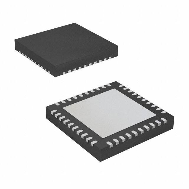


 工商网监
湘ICP备2023018690号
工商网监
湘ICP备2023018690号
