VDD 1
VDETBIAS
21
20
19
PEAK
DETECTOR
16
IN 4
100 Gbps Ethernet LR4 (10 km) and ER4 (40 km) applications
C-form factor pluggable (CFP/CFP2) or similar form factor
modules
Optical transceivers and pluggable modules
Broadband gain stages and preamplifiers
Broadband test and measurement equipment
7
9
VGG
APPLICATIONS
OUT
15331-001
Operation up to 32 Gbps
Low dc power dissipation
0.15 W for 1.5 V p-p swing at 3.5 V supply
0.4 W for 2 V p-p swing at 5 V supply
Adjustable output amplitude from 1.2 V p-p to 2.2 V p-p
Integrated peak detector
24-lead, ceramic, 4 mm × 4 mm LCC package: 16 mm2
VDET
FUNCTIONAL BLOCK DIAGRAM
VDETREF
FEATURES
VCTL
Data Sheet
28 Gbps EML Driver with Peak Detector
HMC7144
Figure 1.
GENERAL DESCRIPTION
The HMC7144 is a broadband driver amplifier for electroabsorption modulated lasers (EML). The device supports data rates
up to 28 Gbps to meet 100 Gbps Ethernet system requirements.
The device provides module designers with a scalable power
dissipation for varying drive voltage characteristics of different
modulators; the power consumption of the module can be set as
low as 0.12 W to 0.5 W at 1.5 V p-p and 2.2 V p-p output
amplitudes, respectively.
Rev. C
The HMC7144 supports a wide range of supply voltages from
3.5 V to 7 V and delivers excellent time domain performance. The
driver incorporates the unique peak detector with reference
feature that enables continuous output amplitude monitoring
without the need for external high frequency circuitry. The
output amplitude and crosspoint are adjustable via control pins.
The input and output are 50 Ω and require ac coupling.
The HMC7144 is housed in a robust, leadless, 4 mm × 4 mm
ceramic LCC package.
Document Feedback
Information furnished by Analog Devices is believed to be accurate and reliable. However, no
responsibility is assumed by Analog Devices for its use, nor for any infringements of patents or other
rights of third parties that may result from its use. Specifications subject to change without notice. No
license is granted by implication or otherwise under any patent or patent rights of Analog Devices.
Trademarks and registered trademarks are the property of their respective owners.
One Technology Way, P.O. Box 9106, Norwood, MA 02062-9106, U.S.A.
Tel: 781.329.4700
©2016 Analog Devices, Inc. All rights reserved.
Technical Support
www.analog.com
�HMC7144* PRODUCT PAGE QUICK LINKS
Last Content Update: 02/23/2017
COMPARABLE PARTS
DISCUSSIONS
View a parametric search of comparable parts.
View all HMC7144 EngineerZone Discussions.
EVALUATION KITS
SAMPLE AND BUY
• HMC7144LC4 Evaluation Board
Visit the product page to see pricing options.
DESIGN RESOURCES
TECHNICAL SUPPORT
• HMC7144 Material Declaration
Submit a technical question or find your regional support
number.
• PCN-PDN Information
• Quality And Reliability
• Symbols and Footprints
DOCUMENT FEEDBACK
Submit feedback for this data sheet.
This page is dynamically generated by Analog Devices, Inc., and inserted into this data sheet. A dynamic change to the content on this page will not
trigger a change to either the revision number or the content of the product data sheet. This dynamic page may be frequently modified.
�HMC7144
Data Sheet
TABLE OF CONTENTS
Features .............................................................................................. 1
Interface Schematics .....................................................................7
Applications ....................................................................................... 1
Typical Performance Characteristics ..............................................8
Functional Block Diagram .............................................................. 1
Applications Information .............................................................. 11
General Description ......................................................................... 1
Device Operation ....................................................................... 11
Revision History ............................................................................... 2
Device Power-Up........................................................................ 11
Specifications..................................................................................... 3
Device Power-Down .................................................................. 11
3.5 V Electrical Specifications..................................................... 3
Application Circuit ..................................................................... 11
5.0 V Electrical Specifications..................................................... 4
Evaluation Printed Circuit Board (PCB) ................................ 12
Typical Bias Voltages .................................................................... 4
Outline Dimensions ....................................................................... 13
Absolute Maximum Ratings............................................................ 5
Ordering Guide .......................................................................... 13
ESD Caution .................................................................................. 5
Pin Configuration and Function Descriptions ............................. 6
REVISION HISTORY
This Hittite Microwave Products data sheet has been reformatted
to meet the styles and standards of Analog Devices, Inc.
12/2016—v02.0314 to Rev. C
Changes to Features, Applications, and General Description
Section ................................................................................................ 1
Changes to Table 3 ............................................................................ 4
Changes to Table 4 ............................................................................ 5
Changes to Table 5 ............................................................................ 6
Changes to Device Power-Up Section ......................................... 11
Rev. C | Page 2 of 13
�Data Sheet
HMC7144
SPECIFICATIONS
3.5 V ELECTRICAL SPECIFICATIONS
VDD = 3.5 V, TA = 25°C, unless otherwise noted.
Table 1.
Parameter
MAXIMUM DATA RATE
GAIN
RETURN LOSS
Input
Output
GROUP DELAY VARIATION
ADJUSTABLE OUTPUT SWING RANGE
TIMING
Rise
Fall
JITTER
Additive RMS Jitter1
Deterministic
SIGNAL-TO-NOISE RATIO (SNR)
SUPPLY CURRENT (IDD)
BIAS CURRENT ADJUST/CROSSPOINT ADJUST
Bias Voltage (VGG)
Bias Current (IGG)
OUTPUT AMPLITUDE ADJUST
Voltage (VCTL)
Current (ICTL)
CROSSPOINT RANGE2
PEAK DETECT SENSITIVITY
1
2
Test Conditions/Comments
Min
DC to 10 GHz
10 GHz to 20 GHz
20 GHz to 30 GHz
10
11.8
5.8
DC to 10 GHz
10 GHz to 20 GHz
20 GHz to 30 GHz
DC to 10 GHz
10 GHz to 20 GHz
20 GHz to 30 GHz
DC to 10 GHz
10 GHz to 20 GHz
20 GHz to 30 GHz
Data input = 28 Gbps nonreturn to zero (NRZ) pseudorandom binary sequence (PRBS) 231 − 1 pattern, 0.5 V p-p
Data input = 28 Gbps NRZ PRBS 231 − 1 pattern, 0.5 V p-p
20% to 80%
20% to 80%
Data input = 28 Gbps NRZ PRBS 231 − 1 pattern, 0.5 V p-p
Additive rms jitter is calculated by JRMS DUT = √((JTESTED)2 − (JSOURCE)2) with 28 Gbps 10101 … pattern, 0.5 V p-p.
Adjust VGG between −1 V and 0 V to achieve the desired crosspoint percentage.
Rev. C | Page 3 of 13
Max
32
13.8
13.5
13
Unit
Gbps
dB
dB
dB
−13
−16
−18
−23
−21
−18
±5
±10
±22
−10
−9
−4
−15
−13
−11
dB
dB
dB
dB
dB
dB
ps
ps
ps
V p-p
0.9
1.5
14.5
16.2
240
270
40
23
45
−1.5
ps
ps
55
fS
ps
dB
mA
−0.9
−0.5
1
V
mA
−1
−0.2
45
75
50
85
+0.5
1
55
95
V
mA
%
mV/V
Data input = 28 Gbps NRZ PRBS 231 − 1 pattern, 0.5 V p-p
RLOAD = 10 MΩ at VDET and VDETREF
Typ
28
13
12.8
8.8
320
2
�HMC7144
Data Sheet
5.0 V ELECTRICAL SPECIFICATIONS
VDD = 5.0 V, TA = 25°C, unless otherwise specified.
Table 2.
Parameter
MAXIMUM DATA RATE
GAIN
RETURN LOSS
Input
Output
GROUP DELAY VARIATION
ADJUSTABLE OUTPUT SWING RANGE
TIMING
Rise
Fall
JITTER
Additive RMS Jitter1
Deterministic
SIGNAL-TO-NOISE RATIO (SNR)
SUPPLY CURRENT (IDD)
BIAS CURRENT ADJUST/CROSSPOINT ADJUST
Gate Bias Voltage (VGG)
Gate Bias Current (IGG)
OUTPUT AMPLITUDE ADJUST
Control Bias Voltage (VCTL)
Control Bias Current (ICTL)
CROSSPOINT RANGE2
PEAK DETECT SENSITIVITY
1
2
Test Conditions/Comments
Min
DC to 10 GHz
10 GHz to 20 GHz
20 GHz to 30 GHz
11
10
7
DC to 10 GHz
10 GHz to 20 GHz
20 GHz to 30 GHz
DC to 10 GHz
10 GHz to 20 GHz
20 GHz to 30 GHz
DC to 10 GHz
10 GHz to 20 GHz
20 GHz to 30 GHz
Data input = 28 Gbps NRZ PRBS 231 − 1 pattern, 0.5 V p-p
Data input = 28 Gbps NRZ PRBS 231 − 1 pattern, 0.5 V p-p
20% to 80%
20% to 80%
Data input = 28 Gbps NRZ PRBS 231 − 1 pattern, 0.5 V p-p
Max
32
16
15
13
Unit
Gbps
dB
dB
dB
−13
−14
−16
−23
−21
−15
±6
±10
±20
−10
−10
−7
−10
−10
−7
dB
dB
dB
dB
dB
dB
ps
ps
ps
V p-p
1.2
2.2
15
16
240
250
50
22
70
−1.5
ps
ps
80
fS
ps
dB
mA
−0.85
−0.5
1
V
mA
−1
0
45
75
50
85
+0.5
1
55
95
V
mA
%
mV/V
Data input = 28 Gbps NRZ PRBS 231 − 1 pattern, 0.5 V p-p
RLOAD = 10 MΩ at VDET and VDETREF
Typ
28
15
14
12
310
2
Additive rms jitter is calculated by JRMS DUT = √((JTESTED)2 – (JSOURCE)2) with 28 Gbps 10101 … pattern, 0.5 V p-p.
Adjust VGG between −1 V and 0 V to achieve the desired crosspoint percentage.
TYPICAL BIAS VOLTAGES
Input data amplitude = 500 mV p-p.
Table 3.
Parameter
VDD
3.5 V
4. 0 V
5.0 V
6.0 V
7.0 V
1
VCTL
VGG
IDD
−0.4 V
−0.4 V
0V
−0.2 V
−0.2 V
−0.2 V
−0.9 V
−0.85 V
−0.85 V
−0.8 V
−0.8 V
Set to get IDD
45 mA
53 mA
70 mA
76 mA
92 mA
120 mA1
This value denotes the worst case operating conditions with a maximum case temperature of 87°C.
Rev. C | Page 4 of 13
�Data Sheet
HMC7144
ABSOLUTE MAXIMUM RATINGS
Stresses at or above those listed under Absolute Maximum
Ratings may cause permanent damage to the product. This is a
stress rating only; functional operation of the product at these
or any other conditions above those indicated in the operational
section of this specification is not implied. Operation beyond
the maximum operating conditions for extended periods may
affect product reliability.
Table 4.
Parameter
Drain Bias Voltage (VDD) Range
Gate Bias Voltage (VGG)
Minimum
Maximum
Control Bias Voltage (VCTL)
Minimum
Maximum
Maximum Detector Bias Voltage (VDETBIAS)
Input Voltage Swing (VIN)
Storage Temperature Range
Operating Temperature Range
Maximum Peak Reflow Temperature
Channel Temperature
Thermal Resistance (Channel to Ground Pad)
ESD Sensitivity (Human Body Model)
Rating
12 V
−1.5 V
0V
−1.5 V
2.0 V
2.5 V
2 V p-p
−65°C to +150°C
−40°C to +87°C
260°C
137°C
56.58°C/W
Class 1A
ESD CAUTION
Rev. C | Page 5 of 13
�HMC7144
Data Sheet
20 VDET
19 VDETBIAS
22 NC
21 VDETREF
24 ACG1
23 ACG2
PIN CONFIGURATION AND FUNCTION DESCRIPTIONS
18 GND
VDD 1
GND 2
GND 3
HMC7144
IN 4
TOP VIEW
(Not to Scale)
GND 5
17 GND
16 OUT
15 GND
14 GND
13 GND
NOTES
1. NC = NO CONNECT. NO CONNECTION IS
REQUIRED FOR THESE PINS.
2. EXPOSED PAD. THE EXPOSED PAD
MUST BE CONNECTED TO RF/DC GROUND.
15331-002
9
VGG
ACG4 11
ACG3 12
8
NC
NC 10
7
VCTL
GND 6
Figure 2. Pin Configuration
Table 5. Pin Function Descriptions
Pin No.
1
2, 3, 5, 6, 13 to 15, 17, 18
Mnemonic
VDD
GND
4
7
IN
VCTL
8, 10, 22
9
11
12
16
NC
VGG
ACG4
ACG4
OUT
19
20
21
23
24
VDETBIAS
VDET
VDETREF
ACG2
ACG1
EPAD
Description
Supply Voltage.
Ground. These pins and the die bottom must be connected to RF/dc ground. See Figure 3 for the
GND interface schematic.
Input. Pin 4 is dc-coupled and matched to 50 Ω (see Figure 6).
Gate Control Voltage. This pin controls the output voltage swing of the amplifier. The typical value
for VCTL is −0.2 V. See Figure 5.
No Connect. No connection is required for these pins.
Gate Control Voltage, Current.
Low Frequency Termination. Attach bypass capacitors per the application circuit shown in Figure 5.
Low Frequency Termination. Attach bypass capacitors per the application circuit shown in Figure 5.
Output. Pin 16 is decoupled and matched to 50 Ω (see Figure 7). The data polarity of the OUT pin
is the inverse of the data polarity on the IN pin.
Detector Bias Voltage. Set Pin 19 to 1.2 V (see Figure 7).
Detector Output Voltage.
Detector Reference Voltage (see Figure 7).
Low Frequency Termination. Attach bypass capacitors per the application circuit shown in Figure 4.
Low Frequency Termination. Attach bypass capacitors per the application circuit shown in Figure 4.
Exposed Pad. The exposed pad must be connected to RF/dc ground.
Rev. C | Page 6 of 13
�Data Sheet
HMC7144
IN
Figure 3. GND Interface Schematic
15331-006
GND
15331-003
INTERFACE SCHEMATICS
Figure 6. IN Interface Schematic
VDETBIAS
ACG1 ACG2
VCTL
15331-004
VDETREF
VDETREF
OUT
VGG
Figure 7. VDETBIAS, VDETREF, and OUT Interface Schematic
15331-005
ACG3 ACG4
15331-007
Figure 4. ACG1, ACG2, and VCTL Interface Schematic
Figure 5. ACG3, ACG4, and VGG Interface Schematic
Rev. C | Page 7 of 13
�HMC7144
Data Sheet
15331-011
15331-008
TYPICAL PERFORMANCE CHARACTERISTICS
Figure 8. 28 Gbps NRZ PRBS 231 − 1 Pattern Input Data, Input Eye Diagram,
VIN = 510 mV p-p
15331-012
15331-009
Figure 11. 28 Gbps Output Eye Diagram at VDD = 4.0 V, VCTL = −0.2 V,
VGG = −0.89 V, IDD = 50 mA, VOUT = 1.77 V p-p, PDISS = 0.20 W
Figure 9. 28 Gbps Output Eye Diagram at VDD = 3.5 V, VCTL = −0.3 V,
VGG = −0.9 V, IDD = 44 mA, VOUT = 1.59 V p-p, PDISS = 0.15 W
Figure 12. 28 Gbps Output Eye Diagram at VDD = 6.0 V, VCTL = −0.03 V,
VGG = −0.81 V, IDD = 79 mA, VOUT = 2.37 V p-p, PDISS = 0.47 W
20
3.5V
4.0V
5.0V
6.0V
18
16
GAIN (dB)
14
12
10
8
6
2
0
DATA INPUT = 28Gbps NRZ PRBS 231 – 1 PATTERN 0.5V p-p
0
2
4
6
8
10 12 14 16 18 20 22 24 26 28 30
FREQUENCY (GHz)
Figure 10. 28 Gbps Output Eye Diagram at VDD = 5.0 V, VCTL = −0.05 V,
VGG = −0.85 V, IDD = 64 mA, VOUT = 2.09 V p-p, PDISS = 0.32 W
Figure 13. Gain over Supply, VGG = −0.90 V
Rev. C | Page 8 of 13
15331-013
15331-010
4
�Data Sheet
INPUT RETURN LOSS (dB)
–5
0
400
–5
390
–10
–10
–15
–15
–20
–20
–25
–25
–30
–30
–35
–35
–40°C
+25°C
+87°C
380
GROUP DELAY (ps)
–40°C
+25°C
+87°C
OUTPUT RETURN LOSS (dB)
0
HMC7144
370
360
350
340
2
4
6
–40
10 12 14 16 18 20 22 24 26 28 30
8
FREQUENCY (GHz)
320
0
2
4
6
8
10 12 14 16 18 20 22 24 26 28 30
FREQUENCY (GHz)
Figure 17. Group Delay vs. Frequency over Temperature, VGG = −0.90 V,
VDD = 5 V (See Table 3 for Typical Bias Voltages)
Figure 14. Input and Output Return Loss over Temperature, VDD = 5 V
(See Table 3 for Typical Bias Voltages)
2.5
2.5
–40°C
+25°C
+87°C
3.5V
4.0V
5.0V
6.0V
2.0
OUTPUT SWING (V p-p)
1.5
1.0
1.5
1.0
0.5
0.5
VCTL (V)
DATA INPUT = 28Gbps NRZ PRBS 231 – 1 PATTERN 0.5V p-p
0
–0.8
–0.6
–0.4
–0.2
0
15331-015
DATA INPUT = 28Gbps NRZ PRBS 231 – 1 PATTERN 0.5V p-p
0
–0.8
–0.6
–0.4
–0.2
0
VCTL (V)
Figure 18. Output Swing vs. VCTL over Supply, VGG = −0.90 V,
Data Input = 28 Gbps NRZ PRBS 231 – 1 Pattern, 0.5 V p-p
Figure 15. Output Swing vs. VCTL over Temperature, VGG = −0.90 V, Data
Input = 28 Gbps NRZ PRBS 231 − 1 Pattern, 0.5 V p-p, VDD = 5 V (See Table 3
for Typical Bias Voltages)
20
0.40
–40°C
+25°C
+87°C
18
0.35
POWER DISSIPATION (W)
16
14
12
10
8
6
15331-018
OUTPUT SWING (V p-p)
2.0
GAIN (dB)
15331-017
0
15331-014
330
–40
–40°C
+25°C
+87°C
0.30
0.25
0.20
0.15
0.10
4
0
2
4
6
8
10 12 14 16 18 20 22 24 26 28 30
FREQUENCY (GHz)
DATA INPUT = 28Gbps NRZ PRBS 231 – 1 PATTERN 0.5V p-p
0
0.5
1.0
1.5
2.0
2.5
15331-016
0
Figure 16. Gain over Temperature, VDD = 5 V (See Table 3 for Typical Bias
Voltages)
OUTPUT SWING (V p-p)
15331-019
0.05
2
Figure 19. Power Dissipation vs. Output Swing over Temperature, VDD = 5 V
(See Table 3 for Typical Bias Voltages), Data Input = 28 Gbps NRZ
PRBS 231 − 1 Pattern, 0.5 V p-p
Rev. C | Page 9 of 13
�HMC7144
0.40
0.35
0.30
0.30
RMS JITTER (ps)
0.35
0.20
0.15
0.10
0.9
TOTAL PEAK-TO-PEAK SOURCE JITTER IS J p-p (SOURCE) = 5ps,
DATA INPUT = 0.5V p-p, 28Gbps 1010... PATTERN FOR RMS JITTER,
DATA INPUT = 0.5V p-p, 28Gbps NRZ PRBS 231 − 1 PATTERN
FOR PEAK-TO-PEAK JITTER,
ADDITIVE RMS JITTER IS J RMS = √((JTESTED)2 – (JSOURCE)2)
1.0
1.1
1.2
1.3
1.4
1.5
1.6
1.7
1.8
1.9
2.0
2.1
Figure 20. RMS Jitter vs. Output Swing over Temperature, VDD = 5 V (See
Table 3 for Typical Bias Voltages), Total Peak-to-Peak Source Jitter is
Jp-p(SOURCE) = 5 ps, Data Input = 0.5 V p-p, 28 Gbps 1010 … Pattern for RMS
Jitter, Data Input = 0.5 V p-p, 28 Gbps NRZ PRBS 231 − 1 Pattern for Peak-ToPeak Jitter, Additive RMS Jitter is JRMS = √((JTESTED)2 – (JSOURCE)2)
PEAK DETECT VOLTAGE (mV)
DATA INPUT = 28Gbps NRZ PRBS 231 – 1 PATTERN 0.5V p-p
20
0.5
1.0
1.5
2.0
2.5
OUTPUT SWING (V p-p)
Figure 21. Signal-to-Noise Ratio vs. Output Swing over Supply, VGG = −0.90 V,
Data Input = 28 Gbps NRZ PRBS 231 − 1 Pattern, 0.5 V p-p
POWER DISSIPATION (W)
3.5V
4.0V
5.0V
6.0V
150
1.2
1.3
1.4
1.5
1.6
1.7
1.8
1.9
2.0
2.1
10MΩ
5MΩ
1MΩ
100kΩ
10kΩ
50
0
0.5
1.0
1.5
2.0
OUTPUT SWING (V p-p)
2.5
3.0
Figure 24. Peak-Detect Voltage vs. Output Swing over RLOAD, VDD = 5 V (See
Table 3 for Typical Bias Voltages), VDETBIAS = 1.2 V, Peak Detect Voltage =
VDET − VDETREF, RLOAD is Equivalent Resistance to GND at VDET and
VDETREF Pins
0.3
0.2
15331-022
0.1
OUTPUT SWING (V p-p)
1.1
100
0.4
DATA INPUT = 28Gbps NRZ PRBS 231 – 1 PATTERN 0.5V p-p
0
0.5
1.0
1.5
2.0
2.5
1.0
Figure 23. RMS Jitter vs. Output Swing over Supply, VGG = −0.90 V, Total Peakto-Peak Source Jitter is Jp-p(SOURCE) = 5 ps, Data Input = 0.5 V p-p, 28 Gbps 1010
… Pattern for RMS Jitter, Data Input = 0.5 V p-p, 28 Gbps NRZ PRBS 231 − 1
Pattern for Peak-To-Peak Jitter, Additive RMS Jitter is JRMS = √((JTESTED)2 –
(JSOURCE)2)
15331-021
SIGNAL TO NOISE RATIO (dB)
21
TOTAL PEAK-TO-PEAK SOURCE JITTER IS Jp-p (SOURCE) = 5ps,
DATA INPUT = 0.5V p-p, 28Gbps 1010... PATTERN FOR RMS JITTER,
DATA INPUT = 0.5V p-p, 28Gbps NRZ PRBS 231 − 1 PATTERN
FOR PEAK-TO-PEAK JITTER,
ADDITIVE RMS JITTER IS J RMS = √((JTESTED)2 – (JSOURCE)2)
OUTPUT SWING (V p-p)
200
22
0.5
0.10
0.9
3.5V
4.0V
5.0V
6.0V
23
0.6
0.20
0.15
OUTPUT SWING (V p-p)
24
0.25
15331-024
0.25
3.5V
4.0V
5.0V
6.0V
15331-023
–40°C
+25°C
+87°C
15331-020
RMS JITTER (ps)
0.40
Data Sheet
Figure 22. Power Dissipation vs. Output Swing over Supply, VGG = −0.90 V,
Data Input = 28 Gbps NRZ PRBS 231 − 1 Pattern, 0.5 V p-p
Rev. C | Page 10 of 13
�Data Sheet
HMC7144
APPLICATIONS INFORMATION
6.
DEVICE OPERATION
Make necessary adjustments, as follows:
a. VGG can be adjusted to obtained the desired eye
crossing point percentage.
b. VCTL can be adjusted to set the desired output voltage
swing.
c. VDD can be further adjusted to optimize the power
consumption and the output voltage swing.
The HMC7144 is susceptible to damage from electrostatic
discharge. Observe proper precautions during handling,
assembly, and test.
DEVICE POWER-UP
To power-up the device properly, take the following steps:
1.
2.
3.
4.
5.
Ground the device.
Set VGG to −1.3 V to ensure the device is turned off when
supply is applied in Step 4 (no drain current).
Set VCTL to its typical value (see Table 3, no drain
current).
Set VDD to its typical value (see Table 3, no drain current).
Increase VGG until the supply current (IDD) reaches its
desired value.
Note that Step 2 and Step 3 can be performed at the same time,
or Step 3 can be performed before Step 2.
DEVICE POWER-DOWN
Reverse Step 1 through Step 4 listed in the Device Power-Up
section.
APPLICATION CIRCUIT
PEAK DETECT CIRCUIT
6
C7
1nF
GND
TP5
5
4
3
2
1
C6
1nF
C8
1nF
20
19
17
4
15
5
14
6
13
9
16
8
3
C22
100nF
C10
10nF
C2
1nF
GND
C4
1nF
VCTL
TP2
C11
10nF
L1
530nH
R1
475Ω
C18
470nF
C3
1nF
VBIAS
TP4
C23
10µF
EML BIAS CIRCUIT
15331-100
C16
4.7µF
J2
OUT
L2
100µH
PACKAGE
BASE
VCTL
TP2
C15
4.7µF
C19
470nF
18
PEAK
DETECTOR
7
C21
100nF
21
1
2
J1
IN
C5
1nF
12
C1
1nF
11
C9
10nF
10
C14
4.7µF
22
VDD
TP1
23
24
NC
C29
470nF
J3
Figure 25. Evaluation Board Schematic
Rev. C | Page 11 of 13
�HMC7144
Data Sheet
15331-025
EVALUATION PRINTED CIRCUIT BOARD (PCB)
Figure 26. EVAL01-HMC7144LC4 Evaluation PCB
Table 6. Bill of Materials for the EVAL01-HMC7144LC4
Evaluation Board1
Item
J1, J2
J3
TP1 to TP5
C1 to C8
C9 to C11
C14 to C16
C18 to C19, C29
C21, C22
C23
L1
L2
U1
PCB
1
Description
K connector
2 mm, 6-pin SMT header
DC test point
1000 pF capacitor, 0402 package
10 nF capacitor, 0603 package
4.7 μF capacitor, 0603 package
0.47 μF capacitor, 0603 package
47,000 pF capacitor, 0402 package
10 μF capacitor, 1206 package
0.53 μH inductor, conical package
100 μH inductor, 1210 package
HMC7144, 28 Gbps, EML driver with peak
detector
600-00709-00-1 evaluation board, circuit
board material is Rogers 4350 or Arlon 25 FR
The board in this application uses radio frequency (RF) circuit
board design techniques. Provide 50 Ω impedance for the signal
lines and connect the package ground leads and exposed pad
directly to the ground plane, similar to that shown in Figure 26.
Use a sufficient number of via holes to connect the top and
bottom ground planes.
Reference this number to order the full evaluation PCB.
Rev. C | Page 12 of 13
�Data Sheet
HMC7144
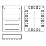
OUTLINE DIMENSIONS
4.13
4.00 SQ
3.87
PIN 1
INDICATOR
0.36
0.30
0.24
PIN 1
(0.32 × 0.32)
19
24
1
18
0.50
BSC
EXPOSED
PAD
2.50 SQ
13
6
7
12
TOP VIEW
BOTTOM VIEW
SIDE VIEW
3.10 BSC
FOR PROPER CONNECTION OF
THE EXPOSED PAD, REFER TO
THE PIN CONFIGURATION AND
FUNCTION DESCRIPTIONS
SECTION OF THIS DATA SHEET.
PKG-004840
SEATING
PLANE
04-03-2015-A
2.50 REF
1.02 MAX
Figure 27. 24-Terminal Ceramic Leadless Chip Carrier [LCC]
(E-24-1)
Dimensions shown in millimeters
ORDERING GUIDE
Package
Option
E-24-1
Model
HMC7144LC4
Temperature Range
−40°C to +87°C
MSL Rating1
MSL3
Package Description2
24-Terminal Ceramic Leadless Chip Carrier
Package [LCC], 50 Pieces Reel
HMC7144LC4TR
−40°C to +87°C
MSL3
24-Terminal Ceramic Leadless Chip Carrier
Package [LCC], 100 Pieces Reel
E-24-1
HMC7144LC4TR-R5
−40°C to +87°C
MSL3
24-Terminal Ceramic Leadless Chip Carrier
Package [LCC], 500 Pieces Reel
E-24-1
EVAL01-HMC7144LC4
Evaluation Board
1
See the Absolute Maximum Ratings section.
Package body material is alumina, white. Lead finish is gold over nickel.
3
XXXX is the 4-digit lot number.
2
©2016 Analog Devices, Inc. All rights reserved. Trademarks and
registered trademarks are the property of their respective owners.
D15331-0-12/16(C)
Rev. C | Page 13 of 13
Branding3
H7144
XXXX
H7144
XXXX
H7144
XXXX
�


 工商网监
湘ICP备2023018690号
工商网监
湘ICP备2023018690号
