HMC816LP4E
v00.1108
Typical Applications
Features
The HMC816LP4E is ideal for:
Low Noise Figure: 0.5 dB
• Cellular/3G and LTE/WiMAX/4G
High Gain: 22 dB
• BTS & Infrastructure
High Output IP3: +37 dBm
• Repeaters and Femtocells
Single Supply: +3V to +5V
• Public Safety Radio
50 Ohm Matched Input/Output
• Multi-Channel Applications
TE
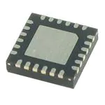
24 Lead 4x4mm QFN Package: 16 mm2
Functional Diagram
General Description
LE
The HMC816LP4E is a GaAs pHEMT Dual Channel
Low Noise Amplifier that is ideal for Cellular/3G and
LTE/WiMAX/4G basestation front-end receivers
operating between 230 and 660 MHz. The amplifier
has been optimized to provide 0.5 dB noise figure,
22 dB gain and +37 dBm output IP3 from a single
supply of +5V. Input and output return losses are
excellent with minimal external matching and bias
decoupling components. The HMC816LP4E shares
the same package and pinout with the HMC817LP4E & HMC818LP4E LNAs. The HMC817LP4E can
be biased with +3V to +5V and features an externally
adjustable supply current which allows the designer
to tailor the linearity performance of each channel of
the LNA for each application.
B
SO
Amplifiers - Low Noise - SMT
7
SMT GaAs pHEMT DUAL CHANNEL
LOW NOISE AMPLIFIER, 230 - 660 MHz
Electrical Specifications, TA = +25° C,
O
Rbias 1, 2 = 10k Ohms*, Vdd = Vdd1, Vdd2 = +5V, Idd = Idd1, Idd2
Parameter
Vdd = +3V
Min.
Frequency Range
Gain
Typ.
Max.
Min.
230 - 450
17
Gain Variation Over Temperature
Vdd = +5V
Typ.
Max.
Min.
450 - 660
21
14
0.001
Min.
19
15
MHz
19
dB
0.007
dB/ °C
0.5
13
17
15
16
dB
Output Return Loss
12
10
13
10
dB
21
dBm
21
dBm
37
dBm
Saturated Output Power (Psat)
10
Output Third Order Intercept (IP3)
Supply Current (Idd)
14
13
16
15
15
14
16.5
16
26
24
34
28
44
24
34
0.9
Units
Noise Figure
10
0.5
Max.
450 - 660
22
0.005
0.9
Typ.
Input Return Loss
Output Power for 1 dB
Compression (P1dB)
0.5
Max.
230 - 450
17
0.002
0.9
Typ.
0.5
19
18
20
18
34
44
68
97
126
68
97
0.9
126
dB
mA
* Rbias sets current, see application circuit herein
7-1
Information furnished by Analog Devices is believed to be accurate and reliable. However, no
For price, delivery,
andRoad,
to place
orders: Analog
Devices,
For price, delivery and to place orders: Hittite Microwave Corporation,
20 Alpha
Chelmsford,
MA
01824Inc.,
responsibility is assumed by Analog Devices for its use, nor for any infringements of patents or other
One Technology Way, P.O. Box 9106, Norwood, MA 02062-9106
rights of third parties that may
result
from
its
use.
Specifications
subject
to
change
without
notice.
No
Phone: 978-250-3343
Fax: 978-250-3373 Phone:
Order 781-329-4700
On-line at www.hittite.com
• Order online at www.analog.com
license is granted by implication or otherwise under any patent or patent rights of Analog Devices.
Application
Support: Phone: 1-800-ANALOG-D
Trademarks and registered trademarks are
the property of their
respective owners.
Application
Support:
Phone: 978-250-3343
or apps@hittite.com
�HMC816LP4E
v00.1108
SMT GaAs pHEMT DUAL CHANNEL
LOW NOISE AMPLIFIER, 230 - 660 MHz
Broadband Gain & Return Loss
20
S21
22
10
GAIN (dB)
Vdd= 5V
Vdd= 3V
5
0
S22
-5
-20
S11
0.2
0.4
0.6
0.8
1
FREQUENCY (GHz)
14
1.2
Gain vs. Temperature [2]
GAIN (dB)
B
SO
+25C
+85C
- 40C
0.25
0.3
0.35
0.4 0.45 0.5 0.55
FREQUENCY (GHz)
0.6
0.65
0.3
0.35
0.4 0.45 0.5 0.55
FREQUENCY (GHz)
0.6
0.65
0.7
O
+25C
+85C
- 40C
-10
-15
-20
0.2
0.25
0.3
0.35
0.4 0.45 0.5 0.55
FREQUENCY (GHz)
0.6
0.65
0.7
Reverse Isolation vs. Temperature [1]
0
0
REVERSE ISOLATION (dB)
-5
+25C
+85C
- 40C
-5
-5
0.7
Output Return Loss vs. Temperature [1]
RETURN LOSS (dB)
0.25
0
22
0.2
0.2
1.4
Input Return Loss vs. Temperature [1]
24
14
+25C
+85C
- 40C
LE
-25
16
18
16
-15
18
20
TE
-10
RETURN LOSS (dB)
RESPONSE (dB)
15
Amplifiers - Low Noise - SMT
24
25
20
7
Gain vs. Temperature [1]
-10
-15
-10
+25C
+85C
- 40C
-15
-20
-25
-30
-35
-40
-20
0.2
0.25
0.3
0.35
0.4 0.45 0.5 0.55
FREQUENCY (GHz)
0.6
0.65
0.7
0.2
0.25
0.3
0.35
0.4 0.45 0.5 0.55
FREQUENCY (GHz)
0.6
0.65
0.7
[1] Vdd = 5V [2] Vdd = 3V
Information
furnisheddelivery
by Analog Devices
believed orders:
to be accurate
and reliable.
However, Corporation,
no
For price, delivery,
andRoad,
to place
orders: Analog
Devices,
For price,
and tois place
Hittite
Microwave
20 Alpha
Chelmsford,
MA
01824Inc.,
responsibility is assumed by Analog Devices for its use, nor for any infringements of patents or other
One Technology Way, P.O. Box 9106, Norwood, MA 02062-9106
rights of third parties that may
result
from
its
use.
Specifications
subject
to
change
without
notice.
No
Phone: 978-250-3343
Fax: 978-250-3373 Phone:
Order781-329-4700
On-line at www.hittite.com
• Order online at www.analog.com
license is granted by implication or otherwise under any patent or patent rights of Analog Devices.
Application
Support: Phone: 1-800-ANALOG-D
Trademarks and registered trademarks are
the property of their
respective owners.
Application
Support:
Phone: 978-250-3343
or apps@hittite.com
7-2
�HMC816LP4E
v00.1108
7
SMT GaAs pHEMT DUAL CHANNEL
LOW NOISE AMPLIFIER, 230 - 660 MHz
Noise Figure vs. Temperature [1]
P1dB vs. Temperature
24
22
+85C
P1dB (dBm)
20
0.6
+25 C
0.4
-40C
0.3
0.4
0.5
0.6
0.2
0.4
LE
IP3 (dBm)
Vdd=3V
+25 C
+85 C
- 40 C
0.25
0.3
0.35
0.4 0.45 0.5 0.55
FREQUENCY (GHz)
0.6
0.65
0.45
0.5
0.55
0.6
0.65
0.7
Vdd=5V
O
35
30
25
+25 C
+85 C
- 40 C
Vdd=3V
20
0.2
0.7
Output IP3 and Supply Current vs.
Supply Voltage @ 400 MHz
0.3
0.4
0.5
0.6
0.7
FREQUENCY (GHz)
Output IP3 and Supply Current vs.
Supply Voltage @ 500 MHz
144
43
140
36
126
40
120
34
108
37
100
32
90
34
80
30
72
28
54
31
60
26
36
28
40
24
18
25
20
0
22
22
2.7
3.1
3.5
3.9
4.3
4.7
5.1
5.5
VOLTAGE SUPPLY (V)
2.7
Idd (mA)
38
Idd (mA)
IP3 (dBm)
0.35
40
Vdd=5V
B
SO
10
0.3
45
22
12
0.25
Output IP3 vs. Temperature
24
14
+25 C
+85 C
- 40 C
FREQUENCY (GHz)
Psat vs. Temperature
16
Vdd=3V
10
0.2
0.7
FREQUENCY (GHz)
18
16
12
0
20
18
TE
Vdd=5V
Vdd=3V
0.2
0.2
Vdd=5V
14
IP3 (dBm)
NOISE FIGURE (dB)
0.8
Psat (dBm)
Amplifiers - Low Noise - SMT
1
0
3.1
3.5
3.9
4.3
4.7
5.1
5.5
VOLTAGE SUPPLY (V)
[1] Measurement reference plane shown on evaluation PCB drawing.
7-3
Information
furnisheddelivery
by Analog Devices
believed orders:
to be accurate
and reliable.
However, no
For price, delivery,
andRoad,
to place
orders: AnalogMA
Devices,
For price,
and tois place
Hittite
Microwave
Corporation,
20 Alpha
Chelmsford,
01824Inc.,
responsibility is assumed by Analog Devices for its use, nor for any infringements of patents or other
One Technology Way, P.O. Box 9106, Norwood, MA 02062-9106
rights of third parties that mayPhone:
result from 978-250-3343
its use. Specifications subject
to
change
without
notice. No
Fax: 978-250-3373
Order781-329-4700
On-line at www.hittite.com
Phone:
•
Order
online
at
www.analog.com
license is granted by implication or otherwise under any patent or patent rights of Analog Devices.
Application
Support: Phone: 1-800-ANALOG-D
Support:
Phone: 978-250-3343
or apps@hittite.com
Trademarks and registered trademarks areApplication
the property of their
respective owners.
�HMC816LP4E
v00.1108
SMT GaAs pHEMT DUAL CHANNEL
LOW NOISE AMPLIFIER, 230 - 660 MHz
Pout
Gain
PAE
35
30
25
20
10
5
0
30
25
20
15
10
5
0
-18
-16
-14
-12
-10
-8
-6
-4
-2
0
2
-18
-16
-14
-12
-10
-8
-6
-4
-2
INPUT POWER (dBm)
LE
INPUT POWER (dBm)
Power Compression @ 500 MHz [2]
Power Compression @ 500 MHz [1]
45
50
40
35
Pout
Gain
PAE
30
25
20
15
10
5
0
-18
B
SO
Pout (dBm), GAIN (dB), PAE (%)
Pout
Gain
PAE
35
TE
15
40
Amplifiers - Low Noise - SMT
40
Pout (dBm), GAIN (dB), PAE (%)
45
-16
-14
-12
-10
-8
-6
-4
-2
0
2
Pout (dBm), GAIN (dB), PAE (%)
Pout (dBm), GAIN (dB), PAE (%)
45
45
40
35
25
20
15
10
5
0
4
-18
-16
-14
-12
Gain
P1dB
1
24
0.8
22
18
0.4
16
14
2.7
Noise Figure
3.1
3.5
3.9
4.3
4.7
SUPPLY VOLTAGE (V)
-8
-6
-4
-2
0
2
5.1
0.2
0
5.5
1
Gain
P1dB
0.8
20
0.6
18
0.4
16
14
2.7
Noise Figure
3.1
3.5
3.9
4.3
4.7
5.1
0.2
NOISE FIGURE (dB)
0.6
NOISE FIGURE (dB)
20
GAIN (dB) & P1dB (dBm)
24
22
-10
INPUT POWER (dBm)
Gain, Power & Noise Figure
vs. Supply Voltage @ 500 MHz
O
Gain, Power & Noise Figure
vs. Supply Voltage @ 400 MHz
Pout
Gain
PAE
30
INPUT POWER (dBm)
GAIN (dB) & P1dB (dBm)
7
Power Compression @ 400 MHz [2]
Power Compression @ 400 MHz [1]
0
5.5
SUPPLY VOLTAGE (V)
[1] Vdd = 5V [2] Vdd = 3V
Information furnished by Analog Devices is believed to be accurate and reliable. However, no
For price, delivery,
andRoad,
to place
orders: AnalogMA
Devices,
For price, delivery and to place orders: Hittite Microwave Corporation,
20 Alpha
Chelmsford,
01824Inc.,
responsibility is assumed by Analog Devices for its use, nor for any infringements of patents or other
One Technology Way, P.O. Box 9106, Norwood, MA 02062-9106
rights of third parties that mayPhone:
result from 978-250-3343
its use. Specifications subject
to
change
without
notice.
No
Fax: 978-250-3373 Phone:
Order781-329-4700
On-line at www.hittite.com
• Order online at www.analog.com
license is granted by implication or otherwise under any patent or patent rights of Analog Devices.
Application
Support: Phone: 1-800-ANALOG-D
Trademarks and registered trademarks areApplication
the property of their
respective owners.
Support:
Phone: 978-250-3343
or apps@hittite.com
7-4
�HMC816LP4E
v00.1108
Output IP3 vs. Rbias @ 500 MHz
40
38
38
36
36
34
34
IP3 (dBm)
40
32
30
26
Vdd= 3V
Vdd= 5V
24
22
500
1000
22
500
10000
1000
LE
Magnitude Balance [1]
0
1
RFIN1 TO RFOUT2
RFIN2 TO RFOUT1
B
SO
-10
0.3
0.4
0.5
0.6
0.7
0.5
0
-0.5
-1
0.2
0.3
FREQUENCY (GHz)
O
2
Vdd (V)
1
0.5
0.6
0.7
3V
Rbias Ω
5V
-1
Idd (mA)
Min
Max
Recommended
4.7k
Open
circuit
10k
34
820
65
0
-2
0.2
0.4
FREQUENCY (GHz)
Absolute Bias Register for Idd
Range & Recommended Bias Resistor
Phase Balance [1]
PHASE BALANCE (degrees)
10000
Rbias (Ohms)
Cross Channel Isolation [1]
-40
0.2
Vdd= 3V
Vdd= 5V
24
Rbias (Ohms)
-30
30
28
26
-20
32
TE
28
AMPLITUDE BALANCE (dB)
IP3 (dBm)
Output IP3 vs. Rbias @ 400 MHz
ISOLATION (dB)
Amplifiers - Low Noise - SMT
7
SMT GaAs pHEMT DUAL CHANNEL
LOW NOISE AMPLIFIER, 230 - 660 MHz
0
Open
circuit
2k
80
3.92k
90
10k
97
With Vdd = 3V Rbias