HMCAD1041-40
v01.0411
Single 10-Bit 20/40 MSPS
A/D Converter
Features
General Description
• 10-bit resolution
The HMCAD1041-40 is a high performance ultra
low power analog-to-digital converter (ADC). The
ADC employs internal reference circuitry, a CMOS
control interface, CMOS output data and is based
on a proprietary structure. Digital error correction is
employed to ensure no missing codes in the complete
full scale range.
• 20/40 MSPS maximum sampling rate
• Ultra-Low Power Dissipation: 15/25 mW
• 61.6 dB SNR @ 8 MHz FIN
• Internal reference circuitry
• 1.8 V core supply voltage
• 1.7 - 3.6 V I/O supply voltage
• Parallel CMOS output
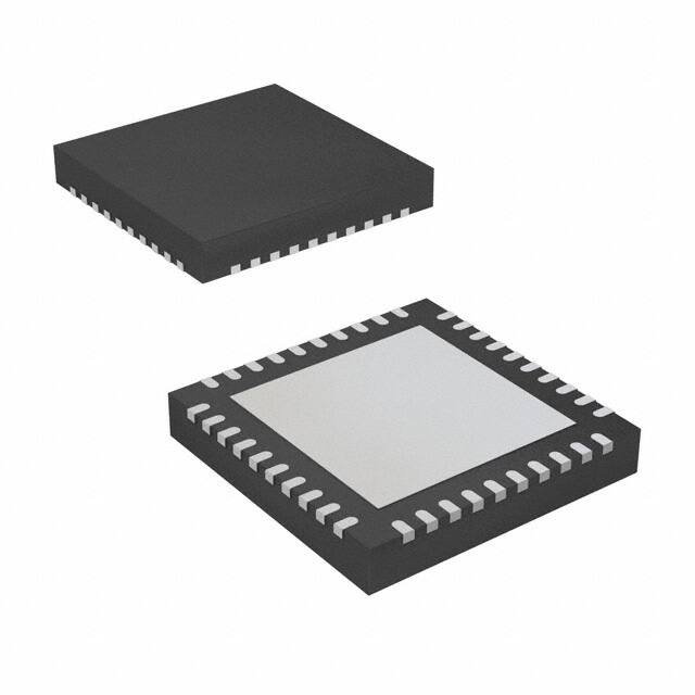
• 6 x 6 mm 40-Pin QFN (LP6HE) Package
A / D Converters - SMT
0
Typical Applications
• Medical Imaging
• Portable Test Equipment
• Digital Oscilloscopes
• IF Communication
Two idle modes with fast startup times exist. The entire
chip can either be put in Standby Mode or Power
Down mode. The two modes are optimized to allow
the user to select the mode resulting in the lowest
possible energy consumption during idle mode and
startup.
The HMCAD1041-40 has a highly linear THA optimized for frequencies up to Nyquist. The differential
clock interface is optimized for low jitter clock sources
and supports LVDS, LVPECL, sine wave and CMOS
clock inputs.
Pin compatible with HMCAD1041-80, HMCAD1051-40
and HMCAD1051-80.
Functional Diagram
Figure 1. Functional Block Diagram
0-1
Information furnished by Analog Devices is believed to be accurate and reliable. However, no
For price, 2delivery,
and to
placeChelmsford,
orders: Analog MA
Devices,
Inc.,
For price,
delivery
and
to place
orders:
Microwave
Corporation,
Elizabeth
Drive,
01824
responsibility
is assumed
by Analog
Devices
for its use,
nor for anyHittite
infringements
of patents or other
One Technology Way, P.O. Box 9106, Norwood, MA 02062-9106
rights of third parties that may result from its use. Specifications subject to change without notice. No
978-250-3343 tel • 978-250-3373 fax • Order
On-line
at www.hittite.com
Phone:
781-329-4700
• Order online at www.analog.com
license is granted by implication or otherwise under any patent or patent rights of Analog Devices.
Application Support: Phone: 1-800-ANALOG-D
Trademarks and registered trademarks are the property of theirApplication
respective owners. Support: apps@hittite.com
�HMCAD1041-40
v01.0411
Single 10-Bit 20/40 MSPS A/D Converter
Electrical Specifications
DC Electrical Specifications
AVDD= 1.8V, DVDD= 1.8V, DVDDCK= 1.8V, OVDD= 2.5V, 20/40 MSPS clock, 50% clock duty cycle, -1 dBFS 8 MHz input signal, unless otherwise noted
Parameter
Condition
Min
Typ
Max
Unit
±6
%FS
DC Accuracy
Guaranteed
Offset error
Midscale offset
Gain error
Full scale range deviation from typical
1
LSB
DNL
Differential nonlinearity
± 0.15
LSB
INL
Integral nonlinearity
± 0.2
LSB
VCM
Common mode voltage output
VAVDD/2
V
Analog Input
VCM -0.1
VCM +0.2
V
Input common mode
Analog input common mode voltage
Full scale range
Differential input voltage range
Input capacitance
Differential input capacitance
Bandwidth
Input Bandwidth
500
Core Supply Voltage
Supply voltage to all 1.8V domain pins. See Pin Configuration and
Description
1.7
1.8
2
V
I/O Supply Voltage
Output driver supply voltage (OVDD). Should be higher than or equal
to Core Supply Voltage (VOVDD ≥ VDVDD)
1.7
2.5
3.6
V
2
Vpp
2
0
pF
MHz
Power Supply
Information furnished by Analog Devices is believed to be accurate and reliable. However, no
For price, 2delivery,
and to
placeChelmsford,
orders: Analog MA
Devices,
Inc.,
For price,
delivery
and
to place
orders:
Microwave
Corporation,
Elizabeth
Drive,
01824
responsibility
is assumed
by Analog
Devices
for its use,
nor for anyHittite
infringements
of patents or other
One Technology Way, P.O. Box 9106, Norwood, MA 02062-9106
rights of third parties that may result from its use. Specifications subject to change without notice. No
978-250-3343 tel • 978-250-3373 fax • Order
On-line
at www.hittite.com
Phone:
781-329-4700
• Order online at www.analog.com
license is granted by implication or otherwise under any patent or patent rights of Analog Devices.
Application Support: Phone: 1-800-ANALOG-D
Trademarks and registered trademarks are the property of theirApplication
respective owners. Support: apps@hittite.com
A / D Converters - SMT
No missing codes
0-2
�HMCAD1041-40
v01.0411
Single 10-Bit 20/40 MSPS A/D Converter
AC Electrical Specifications - 20 MSPS
AVDD=1.8V, DVDD=1.8V, DVDDCK=1.8V, OVDD=2.5V, FS=20MSPS clock, 50% clock duty cycle, -1dBFS 8MHz input signal, unless otherwise noted.
Parameter
Condition
Min
Typ
Max
Unit
Performance
SNR
Signal to Noise Ratio
FIN = 2 MHz
FIN = 8 MHz
SNDR
61.7
60
dBFS
FIN =~ FS/2
61.6
dBFS
FIN = 20 MHz
61.6
dBFS
61.7
dBFS
Signal to Noise and Distortion Ratio
FIN = 2 MHz
FIN = 8 MHz
0
SFDR
60
61.6
dBFS
FIN =~ FS/2
60.5
dBFS
FIN = 20 MHz
61.6
dBFS
80
dBc
Spurious Free Dynamic Range
A / D Converters - SMT
FIN = 2 MHz
FIN = 8 MHz
HD2
70
81
dBc
FIN =~ FS/2
70
dBc
FIN = 20 MHz
80
dBc
-90
dBc
Second order Harmonic Distortion
FIN = 2 MHz
FIN = 8 MHz
HD3
-90
dBc
FIN =~ FS/2
-80
-90
dBc
FIN = 20 MHz
-90
dBc
-80
dBc
Third order Harmonic Distortion
FIN = 2 MHz
FIN = 8 MHz
ENOB
dBFS
61.6
-70
-81
dBc
FIN =~ FS/2
-70
dBc
FIN = 20 MHz
-80
dBc
10
bits
Effective number of Bits
FIN = 2 MHz
FIN = 8 MHz
9.7
9.9
bits
FIN =~ FS/2
9.8
bits
FIN = 20 MHz
9.9
bits
Power Supply
Analog supply current
5.7
mA
Digital core supply
1
mA
Output driver supply
2.5V output driver supply, sine wave input, FIN = 1 MHz, CK_EXT enabled
1.7
mA
Output driver supply
2.5V output driver supply, sine wave input, FIN = 1 MHz, CK_EXT disabled
1.2
mA
Digital supply current
Analog power Dissipation
10.3
mW
Digital power Dissipation
OVDD = 2.5V, 5pF load on output bits, FIN = 1 MHz, CK_EXT disabled
4.8
mW
Total power Dissipation
OVDD = 2.5V, 5pF load on output bits, FIN = 1 MHz, CK_EXT disabled
15.1
mW
Power Down Dissipation
Sleep Mode
Power Dissipation, Sleep mode
9.9
µW
7.7
mW
Clock Inputs
Max. Conversion Rate
Min. Conversion Rate
0-3
20
MSPS
3
MSPS
Information furnished by Analog Devices is believed to be accurate and reliable. However, no
For price, 2delivery,
and to
placeChelmsford,
orders: Analog MA
Devices,
Inc.,
For price,
delivery
and
to place
orders:
Microwave
Corporation,
Elizabeth
Drive,
01824
responsibility
is assumed
by Analog
Devices
for its use,
nor for anyHittite
infringements
of patents or other
One Technology Way, P.O. Box 9106, Norwood, MA 02062-9106
rights of third parties that may result from its use. Specifications subject to change without notice. No
978-250-3343 tel • 978-250-3373 fax • Order
On-line
at www.hittite.com
Phone:
781-329-4700
• Order online at www.analog.com
license is granted by implication or otherwise under any patent or patent rights of Analog Devices.
Application Support: Phone: 1-800-ANALOG-D
Trademarks and registered trademarks are the property of theirApplication
respective owners. Support: apps@hittite.com
�HMCAD1041-40
v01.0411
Single 10-Bit 20/40 MSPS A/D Converter
AC Electrical Specifications - 40 MSPS
AVDD=1.8V, DVDD=1.8V, DVDDCK=1.8V, OVDD=2.5V, FS=40MSPS clock, 50% clock duty cycle, -1dBFS 8MHz input signal, unless otherwise noted.
Parameter
Condition
Min
Typ
Max
Unit
Performance
Signal to Noise Ratio
FIN = 2 MHz
FIN = 8 MHz
SNDR
61.6
60
dBFS
FIN =~ FS/2
61.6
dBFS
FIN = 30 MHz
61.5
dBFS
61.6
dBFS
Signal to Noise and Distortion Ratio
FIN = 2 MHz
FIN = 8 MHz
SFDR
60
61.6
dBFS
FIN =~ FS/2
61.2
dBFS
FIN = 30 MHz
61.4
dBFS
80
dBc
Spurious Free Dynamic Range
FIN = 2 MHz
FIN = 8 MHz
HD2
70
81
dBc
FIN =~ FS/2
72
dBc
FIN = 30 MHz
80
dBc
-90
dBc
Second order Harmonic Distortion
FIN = 2 MHz
FIN = 8 MHz
HD3
-80
-90
dBc
FIN =~ FS/2
-85
dBc
FIN = 30 MHz
-85
dBc
-80
dBc
Third order Harmonic Distortion
FIN = 2 MHz
FIN = 8 MHz
ENOB
dBFS
61.6
-70
-81
dBc
FIN =~ FS/2
-72
dBc
FIN = 30 MHz
-80
dBc
9.9
bits
Effective number of Bits
FIN = 2 MHz
FIN = 8 MHz
9.7
9.9
bits
FIN =~ FS/2
9.9
bits
FIN = 30 MHz
9.9
bits
9.3
mA
1.7
mA
mA
Power Supply
Analog supply current
Digital supply current
Digital core supply
Output driver supply
2.5V output driver supply, sine wave input, FIN = 1 MHz, CK_EXT enabled
3.1
Output driver supply
2.5V output driver supply, sine wave input, FIN = 1 MHz, CK_EXT disabled
2.2
mA
16.7
mW
Analog power Dissipation
Digital power Dissipation
OVDD = 2.5V, 5pF load on output bits, FIN = 1 MHz, CK_EXT disabled
8.6
mW
Total power Dissipation
OVDD = 2.5V, 5pF load on output bits, FIN = 1 MHz, CK_EXT disabled
25.3
mW
9.7
µW
11.3
mW
Power Down Dissipation
Sleep Mode
Power Dissipation, Sleep mode
0
A / D Converters - SMT
SNR
Clock Inputs
Max. Conversion Rate
Min. Conversion Rate
40
MSPS
3
MSPS
Information furnished by Analog Devices is believed to be accurate and reliable. However, no
For price, 2delivery,
and to
placeChelmsford,
orders: Analog MA
Devices,
Inc.,
For price,
delivery
and
to place
orders:
Microwave
Corporation,
Elizabeth
Drive,
01824
responsibility
is assumed
by Analog
Devices
for its use,
nor for anyHittite
infringements
of patents or other
One Technology Way, P.O. Box 9106, Norwood, MA 02062-9106
rights of third parties that may result from its use. Specifications subject to change without notice. No
978-250-3343 tel • 978-250-3373 fax • Order
On-line
at www.hittite.com
Phone:
781-329-4700
• Order online at www.analog.com
license is granted by implication or otherwise under any patent or patent rights of Analog Devices.
Application Support: Phone: 1-800-ANALOG-D
Trademarks and registered trademarks are the property of theirApplication
respective owners. Support: apps@hittite.com
0-4
�HMCAD1041-40
v01.0411
Single 10-Bit 20/40 MSPS A/D Converter
Digital and Timing Specifications
AVDD=1.8V, DVDD=1.8V, DVDDCK=1.8V, OVDD=2.5V, Conversion Rate: Max specified, 50% clock duty cycle, -1dBFS input signal, 5 pF capacitive
load on data outputs, unless otherwise noted
Parameter
Condition
Min
Typ
Max
Unit
80
% high
Clock Inputs
Duty Cycle
20
Compliance
A / D Converters - SMT
0
CMOS, LVDS, LVPECL, Sine Wave
Input range
Differential input swing
0.4
Vpp
Input range
Differential input swing, sine wave clock input
1.6
Vpp
Input common mode
voltage
Keep voltages within ground and voltage of OVDD
0.3
Input capacitance
Differential
VOVDD -0.3
2
V
pF
Timing
TPD
Start up time from Power Down Mode to Active Mode
900
clock
cycles
TSLP
Start up time from Sleep Mode to Active Mode
20
clock
cylcles
TOVR
Out of range recovery time
1
clock
cycles
TAP
Aperture Delay
0.8
ns
Єrms
Aperture jitter
< 0.5
ps
TLAT
Pipeline Delay
12
clock
cycles
TD
Output delay (see timing diagram). 5pF load on output bits
3
10
ns
TDC
Output delay relative to CK_EXT (see timing diagram)
1
6
ns
Logic Inputs
VHI
High Level Input Voltage. VOVDD ≥ 3.0V
2
V
VHI
High Level Input Voltage. VOVDD = 1.7V – 3.0V
0.8 ·VOVDD
V
VLI
Low Level Input Voltage. VOVDD ≥ 3.0V
0
0.8
VLI
Low Level Input Voltage. VOVDD = 1.7V – 3.0V
0
0.2 ·VOVDD
V
IHI
High Level Input leakage Current
±10
µA
ILI
Low Level Input leakage Current
±10
µA
CI
Input Capacitance
3
V
pF
Logic Outputs
VHO
High Level Output Voltage
VLO
Low Level Output Voltage
VOVDD -0.1
0.1
V
V
CL
Max capacitive load. Post-driver supply voltage equal to pre-driver
supply voltage VOVDD = VOCVDD
5
pF
CL
Max capacitive load. Post-driver supply voltage above 2.25V (1)
10
pF
(1) The outputs will be functional with higher loads. However, it is recommended to keep the load on output data bits as low as possible
to keep dynamic currents and resulting switching noise at a minimum
0-5
Information furnished by Analog Devices is believed to be accurate and reliable. However, no
For price, 2delivery,
and to
placeChelmsford,
orders: Analog MA
Devices,
Inc.,
For price,
delivery
and
to place
orders:
Microwave
Corporation,
Elizabeth
Drive,
01824
responsibility
is assumed
by Analog
Devices
for its use,
nor for anyHittite
infringements
of patents or other
One Technology Way, P.O. Box 9106, Norwood, MA 02062-9106
rights of third parties that may result from its use. Specifications subject to change without notice. No
978-250-3343 tel • 978-250-3373 fax • Order
On-line
at www.hittite.com
Phone:
781-329-4700
• Order online at www.analog.com
license is granted by implication or otherwise under any patent or patent rights of Analog Devices.
Application Support: Phone: 1-800-ANALOG-D
Trademarks and registered trademarks are the property of theirApplication
respective owners. Support: apps@hittite.com
�HMCAD1041-40
v01.0411
Single 10-Bit 20/40 MSPS A/D Converter
Timing Diagram
Figure 2: Timing Diagram
Absolute Maximum Ratings
Absolute maximum ratings are limiting values to be applied for short periods of time. Exposure to absolute maximum rating conditions for an extended period of time may reduce device lifetime.
Table 1:
Pin
Pin
Rating
AVDD
VSS
-0.3V to +2.3V
DVDD
VSS
-0.3V to +2.3V
AVSS, DVSSCK, DVSS, OVSS
VSS
-0.3V to +0.3V
OVDD
VSS
-0.3V to +3.9V
IP, IN, analog inputs and outputs
VSS
-0.3V to +2.3V
Digital outputs
VSS
-0.3V to +3.9V
CKP, CKN
VSS
-0.3V to +3.9V
Digital Inputs
VSS
-0.3V to +3.9V
Operating temperature
-40 to +85 ºC
Storage temperature
-60 to +150 ºC
Soldering Profile Qualification
J-STD-020
ELECTROSTATIC SENSITIVE DEVICE
OBSERVE HANDLING PRECAUTIONS
Stresses above those listed under Absolute Maximum
Ratings may cause permanent damage to the device. This
is a stress rating only; functional operation of the device
at these or any other conditions above those indicated in
the operational section of this specification is not implied.
Exposure to absolute maximum rating conditions for
extended periods may affect device reliability.
Information furnished by Analog Devices is believed to be accurate and reliable. However, no
For price, 2delivery,
and to
placeChelmsford,
orders: Analog MA
Devices,
Inc.,
For price,
delivery
and
to place
orders:
Microwave
Corporation,
Elizabeth
Drive,
01824
responsibility
is assumed
by Analog
Devices
for its use,
nor for anyHittite
infringements
of patents or other
One Technology Way, P.O. Box 9106, Norwood, MA 02062-9106
rights of third parties that may result from its use. Specifications subject to change without notice. No
978-250-3343 tel • 978-250-3373 fax • Order
On-line
at www.hittite.com
Phone:
781-329-4700
• Order online at www.analog.com
license is granted by implication or otherwise under any patent or patent rights of Analog Devices.
Application Support: Phone: 1-800-ANALOG-D
Trademarks and registered trademarks are the property of theirApplication
respective owners. Support: apps@hittite.com
A / D Converters - SMT
0
0-6
�HMCAD1041-40
v01.0411
Single 10-Bit 20/40 MSPS A/D Converter
Pin Configuration and Description
A / D Converters - SMT
0
0-7
Figure 3: Package Drawing, QFN 40-pin
Information furnished by Analog Devices is believed to be accurate and reliable. However, no
For price, 2delivery,
and to
placeChelmsford,
orders: Analog MA
Devices,
Inc.,
For price,
delivery
and
to place
orders:
Microwave
Corporation,
Elizabeth
Drive,
01824
responsibility
is assumed
by Analog
Devices
for its use,
nor for anyHittite
infringements
of patents or other
One Technology Way, P.O. Box 9106, Norwood, MA 02062-9106
rights of third parties that may result from its use. Specifications subject to change without notice. No
978-250-3343 tel • 978-250-3373 fax • Order
On-line
at www.hittite.com
Phone:
781-329-4700
• Order online at www.analog.com
license is granted by implication or otherwise under any patent or patent rights of Analog Devices.
Application Support: Phone: 1-800-ANALOG-D
Trademarks and registered trademarks are the property of theirApplication
respective owners. Support: apps@hittite.com
�HMCAD1041-40
v01.0411
Single 10-Bit 20/40 MSPS A/D Converter
Table 2: Pin Function
Name
Description
0
VSS
Ground connection for all power domains. Exposed pad
1, 11, 16
DVDD
Digital and I/O-ring pre driver supply voltage, 1.8V
2
CM_EXT
Common Mode voltage output
3, 4, 7,
AVDD
Analog supply voltage, 1.8V
5, 6
IP, IN
Analog input (non-inverting, inverting)
8
DVDDCK
Clock circuitry supply voltage, 1.8V
9
CKP
Clock input, non-inverting (Format: LVDS, LVPECL, CMOS/TTL, Sine Wave)
10
CKN
Clock input, inverting. For CMOS input on CKP, connect CKN to ground.
12
CK_EXT_EN
CK_EXT signal enabled when low (zero). Tristate when high.
13
DFRMT
Data format selection. 0: Offset Binary, 1: Two’s Complement
14
PD_N
Full chip Power Down mode when Low. All digital outputs reset to zero. After chip power up always apply
Power Down mode before using Active Mode to reset chip.
15
OE_N
Output Enable. Tristate when high
17, 18, 25, 26,
36, 37
OVDD
I/O ring post-driver supply voltage. Voltage range 1.7 to 3.6V
19
NC
20
NC
21
NC
22
D_0
23
D_1
Output Data
24
ORNG
Out of Range flag. High when input signal is out of range
Output Data (LSB)
27
CK_EXT
Output clock signal for data synchronization. CMOS levels
28
D_2
Output Data
29
D_3
Output Data
30
D_4
Output Data
31
D_5
Output Data
32
D_6
Output Data
33
D_7
Output Data
34
D_8
Output Data
35
D_9
Output Data (MSB)
38, 39
40
CM_EXTBC_1,
CM_EXTBC_0
SLP_N
Bias control bits for the buffer driving pin CM_EXT
00:
OFF
01:
50uA
10:
500uA
11:
1mA
0
A / D Converters - SMT
Pin #
Sleep Mode when low
Information furnished by Analog Devices is believed to be accurate and reliable. However, no
For price, 2delivery,
and to
placeChelmsford,
orders: Analog MA
Devices,
Inc.,
For price,
delivery
and
to place
orders:
Microwave
Corporation,
Elizabeth
Drive,
01824
responsibility
is assumed
by Analog
Devices
for its use,
nor for anyHittite
infringements
of patents or other
One Technology Way, P.O. Box 9106, Norwood, MA 02062-9106
rights of third parties that may result from its use. Specifications subject to change without notice. No
978-250-3343 tel • 978-250-3373 fax • Order
On-line
at www.hittite.com
Phone:
781-329-4700
• Order online at www.analog.com
license is granted by implication or otherwise under any patent or patent rights of Analog Devices.
Application Support: Phone: 1-800-ANALOG-D
Trademarks and registered trademarks are the property of theirApplication
respective owners. Support: apps@hittite.com
0-8
�HMCAD1041-40
v01.0411
Single 10-Bit 20/40 MSPS A/D Converter
Recommended Usage
Analog Input
The analog inputs to the HMCAD1041-40 is a switched
capacitor track-and-hold amplifier optimized for differential operation. Operation at common mode voltages
at mid supply is recommended even if performance
will be good for the ranges specified. The CM_EXT pin
provides a voltage suitable as common mode voltage
reference. The internal buffer for the CM_EXT voltage
can be switched off, and driving capabilities can be
changed by using the CM_EXTBC control input.
A / D Converters - SMT
0
Figure 4 shows a simplified drawing of the input network. The signal source must have sufficiently low
output impedance to charge the sampling capacitors
within one clock cycle. A small external resistor (e.g.
22 Ohm) in series with each input is recommended
as it helps reducing transient currents and dampens
ringing behavior. A small differential shunt capacitor at
the chip side of the resistors may be used to provide
dynamic charging currents and may improve performance. The resistors form a low pass filter with the
capacitor, and values must therefore be determined by
requirements for the application.
Figure 4: Input configuration
DC-Coupling
Figure 5 shows a recommended configuration for DCcoupling. Note that the common mode input voltage
must be controlled according to specified values. Preferably, the CM_EXT output should be used as reference to set the common mode voltage.
0-9
Figure 5: DC coupled input with buffer
The input amplifier could be inside a companion chip
or it could be a dedicated amplifier. Several suitable
single ended to differential driver amplifiers exist in the
market. The system designer should make sure the
specifications of the selected amplifier is adequate for
the total system, and that driving capabilities comply
with the HMCAD1041-40 input specifications.
Detailed configuration and usage instructions must be
found in the documentation of the selected driver, and
the values given in figure 5 must be varied according
to the recommendations for the driver.
AC-Coupling
A signal transformer or series capacitors can be used
to make an AC-coupled input network. Figure 6 shows
a recommended configuration using a transformer.
Make sure that a transformer with sufficient linearity is
selected, and that the bandwidth of the transformer is
appropriate. The bandwidth should exceed the sampling rate of the ADC with at least a factor of 10. It is
also important to minimize phase mismatch between
the differential ADC inputs for good HD2 performance.
This type of transformer coupled input is the preferred
configuration for high frequency signals as most differential amplifiers do not have adequate performance at
high frequencies. If the input signal is traveling a long
physical distance from the signal source to the transformer (for example a long cable), kick-backs from the
ADC will also travel along this distance. If these kickbacks are not terminated properly at the source side,
they are reflected and will add to the input signal at the
ADC input. This could reduce the ADC performance.
To avoid this effect, the source must effectively terminate the ADC kick-backs, or the traveling distance
should be very short. If this problem could not be
avoided, the circuit in figure 8 can be used.
Information furnished by Analog Devices is believed to be accurate and reliable. However, no
For price, 2delivery,
and to
placeChelmsford,
orders: Analog MA
Devices,
Inc.,
For price,
delivery
and
to place
orders:
Microwave
Corporation,
Elizabeth
Drive,
01824
responsibility
is assumed
by Analog
Devices
for its use,
nor for anyHittite
infringements
of patents or other
One Technology Way, P.O. Box 9106, Norwood, MA 02062-9106
rights of third parties that may result from its use. Specifications subject to change without notice. No
978-250-3343 tel • 978-250-3373 fax • Order
On-line
at www.hittite.com
Phone:
781-329-4700
• Order online at www.analog.com
license is granted by implication or otherwise under any patent or patent rights of Analog Devices.
Application Support: Phone: 1-800-ANALOG-D
Trademarks and registered trademarks are the property of theirApplication
respective owners. Support: apps@hittite.com
�HMCAD1041-40
v01.0411
Single 10-Bit 20/40 MSPS A/D Converter
Figure 8: Alternative input network
Figure 7 shows AC-coupling using capacitors. Resistors from the CM_EXT output, RCM, should be used
to bias the differential input signals to the correct voltage. The series capacitor, CI, form the high-pass pole
with these resistors, and the values must therefore be
determined based on the requirement to the high-pass
cut-off frequency.
Figure 7: AC coupled input
Note that startup time from Sleep Mode and Power
Down Mode will be affected by this filter as the time
required to charge the series capacitors is dependent
on the filter cut-off frequency.
If the input signal has a long traveling distance, and the
kick-backs from the ADC not are effectively terminated
at the signal source, the input network of figure 8 can
be used. The configuration in figure 8 is designed to
attenuate the kickback from the ADC and to provide
an input impedance that looks as resistive as possible
for frequencies below Nyquist. Values of the series
inductor will however depend on board design and
conversion rate. In some instances a shunt capacitor in parallel with the termination resistor (e.g. 33pF)
may improve ADC performance further. This capacitor
attenuate the ADC kick-back even more, and minimize
the kicks traveling towards the source. However, the
impedance match seen into the transformer becomes
worse.
Clock Input and Jitter Considerations
Typically high-speed ADCs use both clock edges to
generate internal timing signals. In the HMCAD104140 only the rising edge of the clock is used. Hence,
input clock duty cycles between 20% and 80% are
acceptable.
The input clock can be supplied in a variety of formats.
The clock pins are AC-coupled internally. Hence a
wide common mode voltage range is accepted. Differential clock sources as LVDS, LVPECL or differential
sine wave can be connected directly to the input pins.
For CMOS inputs, the CKN pin should be connected
to ground, and the CMOS clock signal should be connected to CKP. For differential sine wave clock, the
input amplitude must be at least ± 800 mVpp.
The quality of the input clock is extremely important
for high-speed, high-resolution ADCs. The contribution to SNR from clock jitter with a full scale signal at a
given frequency is shown in equation 1,
SNRjitter = 20 · log (2 · π · ƒIN · єt)
(1)
where fIN is the signal frequency, and εt is the total
rms jitter measured in seconds. The rms jitter is the
total of all jitter sources including the clock generation
circuitry, clock distribution and internal ADC circuitry.
For applications where jitter may limit the obtainable
performance, it is of utmost importance to limit the
clock jitter. This can be obtained by using precise and
stable clock references (e.g. crystal oscillators with
good jitter specifications) and make sure the clock distribution is well controlled. It might be advantageous
to use analog power and ground planes to ensure
low noise on the supplies to all circuitry in the clock
distribution. It is of utmost importance to avoid crosstalk between the ADC output bits and the clock and
between the analog input signal and the clock since
such crosstalk often results in harmonic distortion.
0
A / D Converters - SMT
Figure 6: Transformer coupled input
The jitter performance is improved with reduced rise
and fall times of the input clock. Hence, optimum jitter
performance is obtained with LVDS or LVPECL clock
with fast edges. CMOS and sine wave clock inputs will
result in slightly degraded jitter performance.
Information furnished by Analog Devices is believed to be accurate and reliable. However, no
For price, 2delivery,
and to
placeChelmsford,
orders: Analog MA
Devices,
Inc.,
For price,
delivery
and
to place
orders:
Microwave
Corporation,
Elizabeth
Drive,
01824
responsibility
is assumed
by Analog
Devices
for its use,
nor for anyHittite
infringements
of patents or other
One Technology Way, P.O. Box 9106, Norwood, MA 02062-9106
rights of third parties that may result from its use. Specifications subject to change without notice. No
978-250-3343 tel • 978-250-3373 fax • Order
On-line
at www.hittite.com
Phone:
781-329-4700
• Order online at www.analog.com
license is granted by implication or otherwise under any patent or patent rights of Analog Devices.
Application Support: Phone: 1-800-ANALOG-D
Trademarks and registered trademarks are the property of theirApplication
respective owners. Support: apps@hittite.com
0 - 10
�HMCAD1041-40
v01.0411
Single 10-Bit 20/40 MSPS A/D Converter
If the clock is generated by other circuitry, it should
be re-timed with a low jitter master clock as the last
operation before it is applied to the ADC clock input.
Digital Outputs
0
The timing is described in the Timing Diagram section.
Note that the load or equivalent delay on CK_EXT
always should be lower than the load on data outputs
to ensure sufficient timing margins.
A / D Converters - SMT
Digital output data are presented on parallel CMOS
form. The voltage on the OVDD pin set the levels of the
CMOS outputs. The output drivers are dimensioned to
drive a wide range of loads for OVDD above 2.25V,
but it is recommended to minimize the load to ensure
as low transient switching currents and resulting noise
as possible. In applications with a large fanout or large
capacitive loads, it is recommended to add external
buffers located close to the ADC chip.
The digital outputs can be set in tristate mode by setting the OE_N signal high.
Data Format Selection
The output data are presented on offset binary form
when DFRMT is low (connect to OVSS). Setting
DFRMT high (connect to OVDD) results in 2’s complement output format. Details are shown in table 3.
Table 3: Data Format Description for 2Vpp Full Scale Range
Differential Input Voltage (IP - IN)
Output Data: D_9 : D_0
(DFRMT = 0, Offset Binary)
Output Data: D_9 : D_0
(DFRMT = 1, 2’s Complement)
1.0 V
11 1111 1111
01 1111 1111
+0.24mV
10 0000 0000
00 0000 0000
-0.24mV
01 1111 1111
11 1111 1111
-1.0V
00 0000 0000
10 0000 0000
Reference Voltages
The reference voltages are internally generated and
buffered based on a bandgap voltage reference. No
external decoupling is necessary, and the reference
voltages are not available externally. This simplifies
usage of the ADC since two extremely sensitive pins,
otherwise needed, are removed from the interface.
Operational Modes
The operational modes are controlled with the PD_N
and SLP_N pins. If PD_N is set low, all other control
pins are overridden and the chip is set in Power Down
mode. In this mode all circuitry is completely turned off
and the internal clock is disabled. Hence, only leakage current contributes to the Power Down Dissipation. The startup time from this mode is longer than
for Sleep Mode as all references need to settle to their
final values before normal operation can resume.
The SLP_N signal can be used to set the full chip in
Sleep Mode. In this mode internal clocking is disabled,
but some low bandwidth circuitry is kept on to allow for
0 - 11
The HMCAD1041-40 employs digital offset correction. This means that the output code will be 4096 with
shorted inputs. However, small mismatches in parasitics at the input can cause this to alter slightly. The
offset correction also results in possible loss of codes
at the edges of the full scale range. With no offset
correction, the ADC would clip in one end before the
other, in practice resulting in code loss at the opposite end. With the output being centered digitally, the
output will clip, and the out of range flags will be set,
before max code is reached. When out of range flags
are set, the code is forced to all ones for overrange
and all zeros for underrange.
a short startup time. However, Sleep Mode represents
a significant reduction in supply current, and it can be
used to save power even for short idle periods.
The input clock should be kept running in all idle
modes. However, even lower power dissipation is possible in Power Down mode if the input clock is stopped.
In this case it is important to start the input clock prior
to enabling active mode.
Startup Initialization
The HMCAD1041-40 must be reset prior to normal
operation. This is required every time the power
supply voltage has been switched off. A reset is performed by applying Power Down mode. Wait until a
stable supply voltage has been reached, and pull the
PD_N pin for the duration of at least one clock cycle.
The input clock must be running continuously during
this Power Down period and until active operation
is reached. Alternatively the PD pin can be kept low
during power-up, and then be set high when the power
supply voltage is stable.
Information furnished by Analog Devices is believed to be accurate and reliable. However, no
For price, 2delivery,
and to
placeChelmsford,
orders: Analog MA
Devices,
Inc.,
For price,
delivery
and
to place
orders:
Microwave
Corporation,
Elizabeth
Drive,
01824
responsibility
is assumed
by Analog
Devices
for its use,
nor for anyHittite
infringements
of patents or other
One Technology Way, P.O. Box 9106, Norwood, MA 02062-9106
rights of third parties that may result from its use. Specifications subject to change without notice. No
978-250-3343 tel • 978-250-3373 fax • Order
On-line
at www.hittite.com
Phone:
781-329-4700
• Order online at www.analog.com
license is granted by implication or otherwise under any patent or patent rights of Analog Devices.
Application Support: Phone: 1-800-ANALOG-D
Trademarks and registered trademarks are the property of theirApplication
respective owners. Support: apps@hittite.com
�HMCAD1041-40
v01.0411
Single 10-Bit 20/40 MSPS A/D Converter
Outline Drawing
Table 4: 6x6 mm QFN (40 Pin LP6H) Dimensions
Symbol
Millimeter
Min
Typ
A
A1
Inch
Max
Typ
0.9
0.01
0.05
A2
0.65
0.7
A3
0.2 REF
b
Min
0
0.2
0.25
Max
0.035
0
0.000
0.002
0.026
0.028
0.008 REF
0.32
0.008
0.01
D
6.00 bsc
0.236 bsc
D1
5.75 bsc
0.226 bsc
0.013
D2
3.95
4.1
4.25
0.156
0.162
0.167
L
0.3
0.4
0.5
0.012
0.016
0.02
e
0.50 bsc
Θ1
0°
F
0.2
G
0.24
A / D Converters - SMT
0
0.020 bsc
12°
0°
12°
0.008
0.42
0.6
0.010
0.017
0.024
Package Information
Part Number
Package Body Material
Lead Finish
MSL [1]
Package Marking [2]
HMCAD1041-40
RoHS-compliant Low Stress Injection Molded Plastic
100% matte Sn
Level 2A
ASD0401
XXXX
XXXX
[1] MSL, Peak Temp: The moisture sensitivity level rating classified according to the JEDEC industry standard and to peak solder temperature.
[2] Proprietary marking XXXX, 4-Digit lot number XXXX
Information furnished by Analog Devices is believed to be accurate and reliable. However, no
For price, 2delivery,
and to
placeChelmsford,
orders: Analog MA
Devices,
Inc.,
For price,
delivery
and
to place
orders:
Microwave
Corporation,
Elizabeth
Drive,
01824
responsibility
is assumed
by Analog
Devices
for its use,
nor for anyHittite
infringements
of patents or other
One Technology Way, P.O. Box 9106, Norwood, MA 02062-9106
rights of third parties that may result from its use. Specifications subject to change without notice. No
978-250-3343 tel • 978-250-3373 fax • Order
On-line
at www.hittite.com
Phone:
781-329-4700
• Order online at www.analog.com
license is granted by implication or otherwise under any patent or patent rights of Analog Devices.
Application Support: Phone: 1-800-ANALOG-D
Trademarks and registered trademarks are the property of theirApplication
respective owners. Support: apps@hittite.com
0 - 12
�