HMCAD1102
v03.0611
Octal 12-Bit 80 MSPS
A/D Converter
Features
Typical Applications
• 80 MSPS Maximum Sampling Rate
• Medical Imaging
• Ultra Low Power Dissipation
59 mW/Channel at 80MSPS
• Wireless Infrastructure
• Test and Measurement
• 70.1 dB SNR at 8 MHz FIN
• Instrumentation
• 0.5 µs Startup from Sleep
15 µs from Power Down
• Reduced Power Dissipation Modes Available
• Internal Reference Circuitry
with No External Components Required
0
Pin Compatible Parts
• HMCAD1101
• HMCAD1100
• Coarse and Fine Gain Control
• HMCAD1100/01-AC specifications are
also valid for HMCAD1102
• Internal Offset Correction
• 1.8V Supply Voltage
A / D Converters - SMT
• Serial 12-Bit LVDS Output
• 14-bit LVDS Output Available Up to 65MSPS
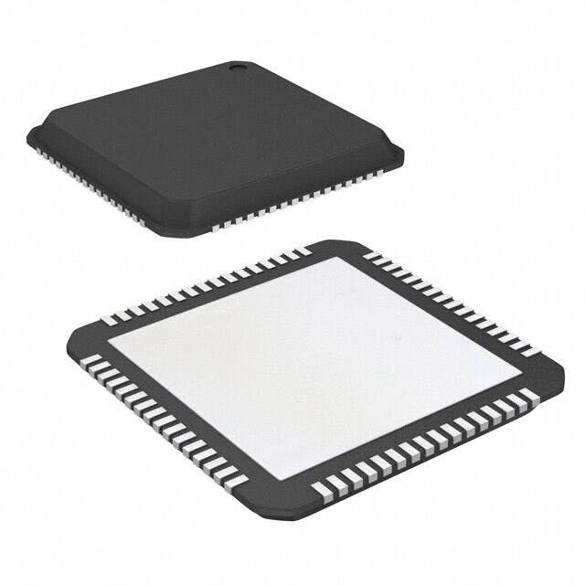
• 64 Lead 9 x 9 mm SMT Package
Functional Diagram
Figure 1. Functional Block Diagram
0-1
Information furnished by Analog Devices is believed to be accurate and reliable. However, no
For price, 2delivery,
and to
placeChelmsford,
orders: Analog MA
Devices,
Inc.,
For price,
delivery
and
to place
orders:
Microwave
Corporation,
Elizabeth
Drive,
01824
responsibility
is assumed
by Analog
Devices
for its use,
nor for anyHittite
infringements
of patents or other
One Technology Way, P.O. Box 9106, Norwood, MA 02062-9106
rights of third parties that may result from its use. Specifications subject to change without notice. No
978-250-3343 tel • 978-250-3373 fax • Order
On-line
at www.hittite.com
Phone:
781-329-4700
• Order online at www.analog.com
license is granted by implication or otherwise under any patent or patent rights of Analog Devices.
Application Support: Phone: 1-800-ANALOG-D
Trademarks and registered trademarks are the property of theirApplication
respective owners. Support: apps@hittite.com
�HMCAD1102
v03.0611
Octal 12-Bit 80 MSPS
A/D Converter
General Description
HMCAD1102 is a high performance low power octal analog-to-digital converter (ADC). The ADC is based on a
proprietary structure and employs internal reference circuitry, a serial control interface and serial LVDS output data.
Data and frame synchronization output clocks are supplied for data capture at the receiver.
Various modes and configuration settings can be applied to the ADC through the serial control interface (SPI). Each
channel can be powered down independently and data format can be selected through this interface. A full chip idle
mode can be set by a single external pin. Register settings determine the exact function of this external pin.
The HMCAD1102 is designed to easily interface with field-programmable gate arrays (FPGAs) from several vendors.
The very low start up times for the HMCAD1102 allows significant power reduction in duty-cycled systems, by utilizing
the Sleep Modes or Power Down Mode when the receive path is idle.
0
Electrical Specifications
AVDD = 1.8V, DVDD = 1.8V, OVDD = 1.8V, 80 MSPS clock, 50% clock duty cycle, -1 dBFS 8 MHz input signal, 12 bit output, unless otherwise noted
Parameter
Description
Min
Typ
Max
Unit
DC accuracy
No Missing Codes
Offset Error
Guaranteed
Offset error after internal digital offset correction
1
Gain Error
LSB
±6
%FS
Gain matching between channels. ±3sigma
value at worst case conditions
±0.5
%FS
DNL
Differential nonlinearity (12-bit level)
±0.2
LSB
INL
Integral nonlinearity (12-bit level)
±0.6
LSB
VCM
Common mode voltage output
VAVDD/2
Gain Matching
Analog Input
Input Common Mode
Analog input common mode voltage
Full Scale Range
Differential input voltage range
Input Capacitance
Differential input capacitance
Bandwidth
Input Bandwidth
VCM -0.1
VCM +0.2
2
V
Vpp
2
pF
500
A / D Converters - SMT
DC Electrical Specifications
MHz
Power Supply
Analog Supply Voltage
1.7
1.8
2
V
Digital Supply Voltage
Digital and output driver supply voltage (up to
65 MSPS)
1.7
1.8
2
V
Digital Supply Voltage
Digital and output driver supply voltage (above
65 MSPS)
1.8
1.9
2
V
OVDD Supply Voltage
Digital CMOS Input Supply Voltage
1.7
1.8
3.6
V
Operating free-air temperature
-40
85
°C
Temperature
Operating Temperature
Information furnished by Analog Devices is believed to be accurate and reliable. However, no
For price, 2delivery,
and to
placeChelmsford,
orders: Analog MA
Devices,
Inc.,
For price,
delivery
and
to place
orders:
Microwave
Corporation,
Elizabeth
Drive,
01824
responsibility
is assumed
by Analog
Devices
for its use,
nor for anyHittite
infringements
of patents or other
One Technology Way, P.O. Box 9106, Norwood, MA 02062-9106
rights of third parties that may result from its use. Specifications subject to change without notice. No
978-250-3343 tel • 978-250-3373 fax • Order
On-line
at www.hittite.com
Phone:
781-329-4700
• Order online at www.analog.com
license is granted by implication or otherwise under any patent or patent rights of Analog Devices.
Application Support: Phone: 1-800-ANALOG-D
Trademarks and registered trademarks are the property of theirApplication
respective owners. Support: apps@hittite.com
0-2
�HMCAD1102
v03.0611
Octal 12-Bit 80 MSPS
A/D Converter
AC Electrical Specifications - 80 MSPS
AVDD = 1.8V, DVDD = 1.8V, OVDD = 1.8V, 80 MSPS clock, 50% clock duty cycle, -1 dBFS 8 MHz input signal, 12 bit output, unless otherwise noted
Parameter
Description
Min
Typ
68.5
70.1
dBFS
70
dBFS
69.6
dBFS
69.5
dBFS
77
dBc
76
dBc
90
dBc
90
dBc
77
dBc
76
dBc
FIN = 8 MHz
11.3
bits
FIN = 30 MHz
11.3
bits
Signal applied to 7 channels (FIN0). Measurement taken on one channel with full scale at FIN1.
FIN1=8MHz, FIN0=9.9MHz
95
dBc
173
mA
88
mA
Analog Power
312
mW
Digital Power
158
mW
Total Power Dissipation
470
mW
Max
Unit
Performance
SNR
Signal to Noise Ratio
FIN = 8 MHz
FIN = 30 MHz
SINAD
Signal to Noise and Distortion Ratio
FIN = 8 MHz
68
FIN = 30 MHz
SFDR
0
FIN = 8 MHz
74
FIN = 30 MHz
HD2
A / D Converters - SMT
Spurious Free Dynamic Range
Second order Harmonic Distortion
FIN = 8 MHz
85
FIN = 30 MHz
HD3
Third order Harmonic Distortion
FIN = 8 MHz
75
FIN = 30 MHz
ENOB
Crosstalk
Effective number of Bits
Power Supply
Analog Supply Current
Digital Supply Current
Digital and output driver supply
Power Down
Power down mode dissipation
10
µW
Sleep Mode
Deep sleep mode power dissipation
56
mW
Power dissipation with all channels in sleep channel
mode (Light sleep)
116
mW
Power dissipation savings per channel off
44
mW
Sleep Channel Mode
Sleep Channel Savings
Clock Inputs
Max. Conversion Rate
Min. Conversion Rate
0-3
80
MSPS
20
MSPS
Information furnished by Analog Devices is believed to be accurate and reliable. However, no
For price, 2delivery,
and to
placeChelmsford,
orders: Analog MA
Devices,
Inc.,
For price,
delivery
and
to place
orders:
Microwave
Corporation,
Elizabeth
Drive,
01824
responsibility
is assumed
by Analog
Devices
for its use,
nor for anyHittite
infringements
of patents or other
One Technology Way, P.O. Box 9106, Norwood, MA 02062-9106
rights of third parties that may result from its use. Specifications subject to change without notice. No
978-250-3343 tel • 978-250-3373 fax • Order
On-line
at www.hittite.com
Phone:
781-329-4700
• Order online at www.analog.com
license is granted by implication or otherwise under any patent or patent rights of Analog Devices.
Application Support: Phone: 1-800-ANALOG-D
Trademarks and registered trademarks are the property of theirApplication
respective owners. Support: apps@hittite.com
�HMCAD1102
v03.0611
Octal 12-Bit 80 MSPS
A/D Converter
Digital and Switching Specifications
AVDD = 1.8V, DVDD = 1.8V, OVDD = 1.8V, unless otherwise noted
Parameter
Description
Typ
Min
Max
Unit
80
% high
Clock Inputs
Duty Cycle
20
Compliance
CMOS, LVDS, LVPECL
Input range, diff
Differential input swing
±200
mVpp
Input range, sine
Differential input swing, sine wave clock input
±800
mVpp
Input range, CMOS
Voltage input range CMOS (CLKN connected
to ground)
Keep voltages within ground and voltage of
OVDD
Input capacitance
0.3
Differential
VOVDD -0.3
2
V
pF
Logic inputs (CMOS)
VHI
High Level Input Voltage. VOVDD ≥ 3.0V
2
V
VHI
High Level Input Voltage. VOVDD = 1.7V – 3.0V
0.8 ·VOVDD
V
VLI
Low Level Input Voltage. VOVDD ≥ 3.0V
0
0.8
VLI
Low Level Input Voltage. VOVDD = 1.7V – 3.0V
0
0.2·VOVDD
V
IHI
High Level Input leakage Current
±10
µA
ILI
Low Level Input leakage Current
±10
µA
CI
Input Capacitance
3
V
pF
Data outputs (LVDS)
Compliance
LVDS
VOUT
Differential output voltage
VCM
Output coding
350
mV
Output common mode voltage
1.2
V
Default/optional
Offset Binary/ 2’s complement
Timing Characteristics
Aperture delay
Aperture jitter
TSU
TSLPCH
Start up time from Power Down Mode
and Deep Sleep Mode to Active Mode.
References have reached 99% of final value.
See section “Clock Frequency”
0.8
ns