IA6805E2
29 August 2007
Microprocessor Unit
As of Production Version 00
IA6805E2
Microprocessor Unit
Data Sheet
Copyright © 2007
IA211081401-03
www.Innovasic.com
Customer Support:
Page 1 of 33
1-888-824-4184
©
�IA6805E2
29 August 2007
Microprocessor Unit
As of Production Version 00
FEATURES
•
•
•
•
•
•
•
•
•
•
•
•
Form, Fit, and Function Compatible with the Harris© CDP6805E2CE and
Motorola© MC146805E2
Internal 8-bit Timer with 7-Bit
Programmable Prescaler
On-chip Clock
Memory Mapped I/O
Versatile Interrupt Handling
True Bit Manipulation
Bit Test and Branch Instruction
Vectored Interrupts
Power-saving STOP and WAIT Modes
Fully Static Operation
112 Bytes of RAM
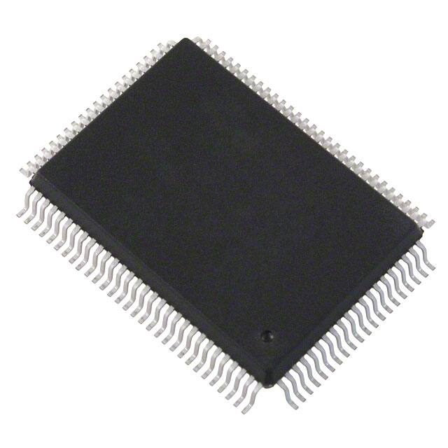
Packaging options available: 40 Pin Plastic DIP or, 44 Pin Plastic
Leaded Chip Carrier, Standard or RoHS packages available
The IA6805E2 is a "plug-and-play" drop-in replacement for the original IC. Innovasic produces replacement
ICs using its MILESTM, or Managed IC Lifetime Extension System, cloning technology. This technology
produces replacement ICs far more complex than "emulation" while ensuring they are compatible with the
original IC. MILESTM captures the design of a clone so it can be produced even as silicon technology
advances. MILESTM also verifies the clone against the original IC so that even the "undocumented features"
are duplicated. This data sheet documents all necessary engineering information about the IA6805E2
including functional and I/O descriptions, electrical characteristics, and applicable timing.
OSC1
TIMER
PB0
(41)
(40)
RESET_N
OSC2
IRQ_N
(1)
(42)
LI
(2)
(43)
DS
DS
(3)
(3)
RW_N
LI
(4)
(2)
NC
(1)
IRQ_N
(5)
RESET_N
(6)
Package Pinout
OSC1
(38)
OSC2
(4)
(37)
TIMER
RW_N
(5)
(36)
PB0
AS
(7)
(39)
PB1
AS
(6)
(35)
PB1
PA7
(8)
(38)
PB2
PA7
(7)
(34)
PB2
PA6
(9)
PA6
(8)
(33)
PB3
PA5
(10)
VDD
VDD
(39)
(44)
(40)
IA6805E2
40 Pin DIP
IA6805E2
44 Pin LCC
(37)
PB3
(36)
PB4
PA5
(9)
(32)
PB4
PA4
(11)
(35)
PB5
PA4
(10)
(31)
PB5
PA3
(12)
(34)
PB6
PA3
(11)
(30)
PB6
PA2
(13)
(33)
PB7
PA2
(12)
(29)
PB7
PA1
(14)
(32)
B0
B4
(23)
B5
A8
(19)
(22)
B6
VSS
(20)
(21)
B7
Copyright © 2007
(28)
(24)
(18)
(27)
(17)
A9
B4
A10
NC
B3
(26)
(25)
B5
(16)
(25)
B3
A11
B6
(29)
(24)
(17)
B7
NC
(23)
B2
VSS
(26)
(22)
(15)
A8
B2
A12
(21)
B1
(30)
A9
(31)
(16)
(20)
(15)
NC
A10
PA0
B1
(19)
B0
(27)
(18)
(28)
(14)
A11
(13)
A12
PA1
PA0
IA211081401-03
www.Innovasic.com
Customer Support:
Page 2 of 33
1-888-824-4184
©
�IA6805E2
29 August 2007
Microprocessor Unit
As of Production Version 00
Description
The IA6805E2 (CMOS) Microprocessor Unit (MPU) is a low cost, low power MPU. It features a
CPU, on-chip RAM, parallel I/O compatibility with pins programmable as input or output. The
following paragraphs will further describe this system block diagram and design in more detail.
TIMER
PRESCALER
OSC1
TIMER/
COUNTER
OSC2
RESET_N
TIMER CONTROL
OSCILLATOR
LI
IRQ_N
PA0
B0
PA0
ACCUMULATOR
PA1
8
CPU
CONTROL
A
PA2
PORT
A
I/O
LINES
PA3
PA4
PORT
A
REG
DATA
DIR
REG
X
PA7
STACK
POINTER
6
PB1
PB2
PB3
PB4
PORT
B
REG
DATA
DIR
REG
B4
MULTIPLEXED
ADDRESS
DATA
BUS
B6
B7
CPU
SP
PROGRAM
COUNTER
HIGH PCH
5
PB0
B3
B5
CONDITION
CODE
5 REGISTER CC
PA5
PA6
PORT
B
I/O
LINES
B2
MUX
BUS
DRIVE
INDEX
REGISTER
8
B1
A8
A9
PROGRAM
COUNTER
LOW PCL
8
ADDRESS
DRIVE
A10
ADDRESS
BUS
A11
A12
ALU
PB5
PB6
PB7
AS
112x8
RAM
BUS
CONTROL
DS
RW_N
ADDRESS STROBE
DATA STROBE
READ/WRITE
Figure 1. System Block Diagram
Copyright © 2007
IA211081401-03
www.Innovasic.com
Customer Support:
Page 3 of 33
1-888-824-4184
©
�IA6805E2
29 August 2007
Microprocessor Unit
As of Production Version 00
I/O Signal Description
The table below describes the I/O characteristics for each signal on the IC. The signal names
correspond to the signal names on the pinout diagrams provided.
S IG N A L N A M E
V DD an d V SS
(P o w e r a n d G ro u n d )
R ESET _n
(R e s e t)
IR Q _ n
(In te rru p t R e q u e s t)
LI
(L o a d In s tru c tio n )
I/O
D E S C R IP T IO N
N /A
S o u rc e : T h e s e tw o p in s p ro v id e p o w e r to th e c h ip .
p o w e r a n d V S S is g ro u n d .
I
T T L : In p u t p in th a t c a n b e u s e d to re s e t th e M P U 's in te rn a l s ta te b y p u llin g th e re s e t_ n
p in lo w .
I
T T L : In p u t p in th a t is le v e l a n d e d g e s e n s itiv e . C a n b e u s e d to re q u e s t a n in te rru p t
sequence.
O
DS
(D a ta S tro b e )
O
R W _n
(R e a d /W rite )
O
AS
(A d d re s s S tro b e )
O
P A 0 -P A 7 /P B 0 -P B 7
(In p u t/O u tp u t L in e s )
I/O
A 8 -A 1 2
(H ig h O rd e r A d d re s s
L in e s )
O
B 0 -B 7
(A d d re s s /D a ta B u s )
I/O
I
T im e r
O SC 1, O SC 2
(S y s te m C lo c k )
I/O
C rys ta l
E x te rn a l C lo c k
V D D p ro v id e s + 5 v o lts (± 0 .5 )
T T L w ith s le w ra te c o n tro l: O u tp u t p in u s e d to in d ic a te th a t a n e x t o p c o d e fe tc h is in
p ro g re s s . U s e d o n ly fo r c e rta in d e b u g g in g a n d te s t s ys te m s . N o t c o n n e c te d in
n o rm a l o p e ra tio n . O v e rla p s D a ta S tro b e (D S ) s ig n a l. T h is o u tp u t is c a p a b le o f d riv in g
o n e s ta n d a rd T T L lo a d a n d 5 0 p F .
T T L w ith s le w ra te c o n tro l: O u tp u t p in u s e d to tra n s fe r d a ta to o r fro m a p e rip h e ra l
o r m e m o ry. D S o c c u rs a n ytim e th e M P U d o e s a d a ta re a d o r w rite a n d d u rin g d a ta
tra n s fe r to o r fro m in te rn a l m e m o ry. D S is a v a ila b le a t f O S C ¸5 w h e n th e M P U is n o t in
th e W A IT o r S T O P m o d e . T h is o u tp u t is c a p a b le o f d riv in g o n e s ta n d a rd T T L lo a d a n d
130pF.
T T L w ith s le w ra te c o n tro l: O u tp u t p in u s e d to in d ic a te th e d ire c tio n o f d a ta tra n s fe r
fro m in te rn a l m e m o ry, I/O re g is te rs , a n d e x te rn a l p e rip h e ra l d e vic e s a n d m e m o rie s .
In d ic a te s to a s e le c te d p e rip h e ra l w h e th e r th e M P U is to re a d (R W _ n h ig h ) o r w rite
(R W _ n lo w ) d a ta o n th e n e x t d a ta s tro b e . T h is o u tp u t is c a p a b le o f d riv in g o n e
s ta n d a rd T T L lo a d a n d 1 3 0 p F .
T T L w ith s le w ra te c o n tro l: O u tp u t s tro b e u s e d to in d ic a te th e p re s e n c e o f a n
a d d re s s o n th e 8 -b it m u ltip le x e d b u s . T h e A S lin e is u s e d to d e m u ltip le x th e e ig h t
le a s t s ig n ific a n t a d d re s s b its fro m th e d a ta b u s . A S is a v a ila b le a t f O S C ¸ 5 w h e n th e
M P U is n o t in th e W A IT o r S T O P m o d e s . T h is o u tp u t is c a p a b le o f d riv in g o n e
s ta n d a rd T T L lo a d a n d 1 3 0 p F .
T T L w ith s le w ra te c o n tro l: T h e s e 1 6 lin e s c o n s titu te In p u t/O u tp u t p o rts A a n d B .
E a c h lin e is in d iv id u a lly p ro g ra m m e d to b e e ith e r a n in p u t o r o u tp u t u n d e r s o ftw a re
c o n tro l o f th e D a ta D ire c tio n R e g is te r (D D R ) a s s h o w n b e lo w in T a b le 1 a n d F ig u re 2 .
T h e p o rt I/O is p ro g ra m m e d b y w ritin g th e c o rre s p o n d in g b it in th e D D R to a "1 " fo r
o u tp u t a n d a "0 " fo r in p u t. In th e o u tp u t m o d e th e b its a re la tc h e d a n d a p p e a r o n th e
c o rre s p o n d in g o u tp u t p in s . A ll th e D D R 's a re in itia lize d to a "0 " o n re s e t. T h e o u tp u t
p o rt re g is te rs a re n o t in itia lize d o n re s e t. E a c h o u tp u t is c a p a b le o f d riv in g o n e
s ta n d a rd T T L lo a d a n d 5 0 p F .
T T L w ith s le w ra te c o n tro l: T h e s e five o u tp u ts c o n s titu te th e h ig h e r o rd e r n o n m u ltip le x e d a d d re s s lin e s . E a c h o u tp u t is c a p a b le o f d riv in g o n e s ta n d a rd T T L lo a d
and 130pF.
T T L w ith s le w ra te c o n tro l: T h e s e b i-d ire c tio n a l lin e s c o n s titu te th e lo w e r o rd e r
a d d re s s e s a n d d a ta . T h e s e lin e s a re m u ltip le x e d w ith a d d re s s p re s e n t a t a d d re s s
s tro b e tim e a n d d a ta p re s e n t a t d a ta s tro b e tim e . W h e n in th e d a ta m o d e , th e s e lin e s
a re b i-d ire c tio n a l, tra n s fe rrin g d a ta to a n d fro m m e m o ry a n d p e rip h e ra l d e v ic e s a s
in d ic a te d b y th e R W _ n p in . A s o u tp u ts , th e s e lin e s a re c a p a b le o f d riv in g o n e
s ta n d a rd T T L lo a d a n d 1 3 0 p F .
T T L : In p u t u s e d to c o n tro l th e in te rn a l tim e r/c o u n te r c irc u itry.
T T L O s c illa to r in p u t/o u tp u t: T h e s e p in s p ro v id e c o n tro l in p u t fo r th e o n -c h ip c lo c k
o s c illa to r c irc u its . E ith e r a c rys ta l o r e x te rn a l c lo c k is c o n n e c te d to th e s e p in s to
p ro v id e a s ys te m c lo c k . T h e c rys ta l c o n n e c tio n is s h o w n in F ig u re 3 . T h e O S C 1 to
b u s tra n s itio n s fo r s ys te m d e s ig n s u s in g o s c illa to rs s lo w e r th a n 5 M H z is s h o w n in
F ig u re 4 .
T h e c irc u it s h o w n in F ig u re 3 is re c o m m e n d e d w h e n u s in g a c rys ta l. A n e x te rn a l
C M O S o s c illa to r is re c o m m e n d e d w h e n u s in g c rys ta ls o u ts id e th e s p e c ifie d ra n g e s .
T o m in im ize o u tp u t d is to rtio n a n d s ta rt-u p s ta b iliza tio n tim e , th e c rys ta l a n d
c o m p o n e n ts s h o u ld b e m o u n te d a s c lo s e to th e in p u t p in s a s p o s s ib le .
W h e n a n e x te rn a l c lo c k is u s e d , it s h o u ld b e a p p lie d to th e O S C 1 in p u t w ith th e O S C 2
in p u t n o t c o n n e c te d , a s s h o w n in F ig u re 3 .
Table 1
Copyright © 2007
IA211081401-03
www.Innovasic.com
Customer Support:
Page 4 of 33
1-888-824-4184
©
�IA6805E2
29 August 2007
Microprocessor Unit
As of Production Version 00
I/O Pin Functions
R/W-n DDR
I/O Pin Functions
0
0
The I/O pin is in input mode. Data is
written into the output data latch.
0
1
Data is written into the output data latch and
output to the I/O pin.
1
0
The state of the I/O pin is read.
1
1
the I/O pin is in an output mode. The
output data latch is read.
I/O Port Circuitry and Register Configuration:
DATA DIRECTION
REGISTER
BIT
TO
AND
LATCHED
OUTPUT
DATA BIT
FROM
I/O
PIN
OUTPUT
CPU
INPUT
REG
BIT
INPUT
I/O
PIN
7
6
5
4
3
2
1
0
DATA DIRECTION
DDA7 DDA6 DDA5 DDA4 DDA3 DDA2 DDA1 DDA0
A(B)
(DDB7) (DDB6) (DDB5) (DDB4) (DDB3) (DDB2) (DDB1) (DDB0)
REGISTER
PORT A(B)
REGISTER
PIN
$0004 ($0005)
$0000 ($0001)
PA7
(PB7)
PA6
(PB6)
PA5
(PB5)
PA4
(PB4)
PA3
(PB3)
PA2
(PB2)
PA1
(PB1)
PA0
(PB0)
Figure 2. PA0-PA7/PB0-PB7 (Input/Output Lines)
Copyright © 2007
IA211081401-03
www.Innovasic.com
Customer Support:
Page 5 of 33
1-888-824-4184
©
�IA6805E2
29 August 2007
Microprocessor Unit
As of Production Version 00
Crystal Parameters Representative Frequencies:
5.0 MHz
50Ω
8 pF
0.02 pF
50 k
15-30 pF
15-25 pF
RS max
C0
C1
Q
COSC1
COSC2
4.0 MHz
75Ω
7 pF
0.012 pF
40 k
15-30 pF
15-25 pF
1.0 MHz
400Ω
5 pF
0.008 pF
30 k
15-40 pF
15-30 pF
Oscillator Connections:
CRYSTAL CIRCUIT
CRYSTAL OSCILLATOR CONNECTIONS
L
C1
38
OSC2
C0
38
NC
10 MΩ
39
OSC1
38
39
38
IA6805E2
OSC1
C OSC1
C OSC2
OSC1
OSC2
39
OSC2
39
OSC2
OSC1
ia6805E2
RS
tOH
tOL
OSC1 PIN
t
tOLOL
Figure 3. OSC1, OSC2 (System Clock)
OSC1 to Bus Transitions Timing Waveforms:
OSC1
AS
DS
RW_n
A[12:8]
B[7:0]
MPU READ
MUX ADDR
B[7:0]
MPU WRITE
MUX ADDR
MPU
READ
DATA*
MPU WRITE DATA
*READ DATA "LATCHED" ON DS FALL
Figure 4. OSC1, OSC2 (System Clock)
Copyright © 2007
IA211081401-03
www.Innovasic.com
Customer Support:
Page 6 of 33
1-888-824-4184
©
�IA6805E2
29 August 2007
Microprocessor Unit
As of Production Version 00
Functional Description
Memory:
The MPU is capable of addressing 8192 bytes of memory and I/O registers. The locations
are divided into internal memory space and external memory space as shown in Figure 5.
The first 128 bytes of memory contain internal port I/O locations, timer locations, and 112
bytes of RAM. The MPU can read from or write to any of these locations. During program
reads from on chip locations, the MPU accepts data only from the addressed on chip
location. Any read data appearing on the input bus is ignored. The shared stack area is used
during interrupts or subroutine calls. A maximum of 64 bytes of RAM is available for stack
usage. The stack pointer is set to $7f at power up. The unused bytes of the stack can be used
for data storage or temporary work locations, but care must be taken to prevent it from
being overwritten due to stacking from an interrupt or subroutine call.
$0000
0
I/O PORTS
TIMER RAM
ACCESS VIA
PAGE 0
DIRECT
ADDRESS
$007F
127
$0080
128
0
PORT A DATA REGISTER
1
PORT B DATA REGISTER
2
EXTERNAL MEMORY SPACE
3
EXTERNAL MEMORY SPACE
4
PORT A DATA DIRECTION REGISTER
5
PORT B DATA DIRECTION REGISTER
6
EXTERNAL MEMORY SPACE
7
EXTERNAL MEMORY SPACE
255
$00FF
8
TIMER DATA REGISTER
256
$0100
9
TIMER CONTROL REGISTER
10
EXTERNAL MEMORY SPACE
15
EXTERNAL MEMORY
SPACE (8064 BYTES)
16
63
64
TIMER INTERRUPT FROM WAIT STATE ONLY
$1FF6 - $1FF7
TIMER INTERRUPT
$1FF8 - $1FF9
EXTERNAL INTERRUPT
$1FFA - $1FFB
SWI
$1FFC - $1FFD
RESET
$1FFE - $1FFF
INTERRUPT
VECTORS
8191
RAM
(112 BYTES)
STACK
(64 BYTES MAX)
127
Figure 5. Memory Map
Copyright © 2007
IA211081401-03
www.Innovasic.com
Customer Support:
Page 7 of 33
1-888-824-4184
©
�IA6805E2
29 August 2007
Microprocessor Unit
As of Production Version 00
Registers:
The following paragraphs describe the registers contained in the MPU. Figure 6 shows the
programming model and Figure 7 shows the interrupt stacking order.
7
0
A
ACCUMULATOR
7
0
X
12
8
7
0
PCL
PCH
12
0
0
0
INDEX REGISTER
0
0
6
1
0
PROGRAM COUNTER
0
SP
4
STACK POINTER
0
CC
H
I
N
Z
C
CONDITION CODE REGISTER
CARRY/BORROW
ZERO
NEGATIVE
INTERRUPT MASK
HALF CARRY
Figure 6. Programming Model
NOTE: Since the stack pointer decrements during pushes, the PCL is stacked first,
followed by PCH, etc. Pulling from the stack is in the reverse order.
STACK
1
INCREASING MEMORY
ADDRESSES
R
E
T
U
R
N
1
1
CONDITION CODE
REGISTER
ACCUMULATOR
INDEX REGISTER
0
0
0
PCH
PCL
I
N
T
E
R
R
U
P
T
DECREASING MEMORY
ADDRESSES
UNSTACK
Figure 7. Interrupt Stacking Order
Copyright © 2007
IA211081401-03
www.Innovasic.com
Customer Support:
Page 8 of 33
1-888-824-4184
©
�IA6805E2
29 August 2007
Microprocessor Unit
As of Production Version 00
A(Accumulator):
The accumulator is an 8-bit register used to hold operands and results of arithmetic
calculations or data manipulations.
X(Index Register):
The index register is an 8-bit register used during the indexed addressing mode. It contains
an 8-bit value used to create an effective address. The index register may also be used as a
temporary storage area when not performing addressing operations.
PC(Program Counter):
The program counter is a 13-bit register that holds the address of the next instruction to be
performed by the MPU.
SP(Stack Pointer):
The stack pointer is a 13-bit register that holds the address of the next free location on the
stack. During an MPU reset or the reset stack pointer (RSP) instruction, the stack pointer is
set to location $007f. The seven most significant bits of the stack pointer are permanently
set to 0000001. They are appended to the six least significant register bits to produce an
address range down to location $0040. The stack pointer gets decremented as data is pushed
onto the stack and incremented as data is removed from the stack. The stack area of RAM is
used to store the return address on subroutine calls and the machine state during interrupts.
The maximum number of locations for the stack pointer is 64 bytes. If the stack goes
beyond this limit the stack pointer wraps around and points to its upper limit thereby losing
the previously stored information. Subroutine calls use 2 bytes of RAM on the stack and
interrupts use 5 bytes.
CC(Condition code Register):
The condition code register is a 5-bit register that indicates the results of the instruction just
executed. The bit is set if it is high. A program can individually test these bits and specific
actions can be taken as a result of their states. Following is an explanation of each bit.
C(Carry Bit):
The carry bit indicates that a carry or borrow out of the Arithmetic Logical Unit (ALU)
occurred during the last arithmetic instruction. This bit is also modified during bit test, shift,
rotate, and branch types of instructions.
Z(Zero Bit):
The zero bit indicates the result of the last arithmetic, logical, or data manipulation was zero.
N(Negative Bit):
The negative bit indicates the result to the last arithmetic, logical, or data manipulation was
negative (bit 7 in the result is high).
Copyright © 2007
IA211081401-03
www.Innovasic.com
Customer Support:
Page 9 of 33
1-888-824-4184
©
�IA6805E2
29 August 2007
Microprocessor Unit
As of Production Version 00
I(Interrupt Mask Bit)
The interrupt mask bit indicates that both the external interrupt and the timer interrupt are
disabled (masked). If an interrupt occurs while this bit is set, the interrupt is latched and is
processed as soon as the interrupt bit is cleared.
H(Half Carry Bit)
The half carry bit indicates that a carry occurred between bits 3 and 4 of the ALU during an
ADD or ADC operation.
Resets:
The MPU can be reset by initial power up or by the external reset pin (reset_n).
POR(Power On Reset)
Power on reset occurs on initial power up. It is strictly for power initialization conditions
and should not be used to detect drops in the power supply voltage. There is a 1920 tCYC
time out delay from the time the oscillator is detected. If the reset_n pin is still low at the
end of the delay, the MPU will remain in the reset state until the external pin goes high.
Reset_n
The reset_n pin is used to reset the MPU. The reset pin must stay low for a minimum of tcyc
to guarantee a reset. The reset_n pin is provided with a Schmitt Trigger to improve noise
immunity capability.
Interrupts:
The MPU can be interrupted with the external interrupt pin (irq_n), the internal timer
interrupt request, or the software interrupt instruction. When any of these interrupts occur,
normal processing is suspended at the end of the current instruction execution. The
processor registers are saved on the stack (stacking order shown in Figure 7) and the
interrupt mask (I) is set to prevent additional interrupts. Normal processing resumes after
the RTI instruction causes the register contents to be recovered from the stack. When the
current instruction is completed, the processor checks all pending hardware interrupts and if
unmasked (I bit clear) proceeds with interrupt processing. Otherwise, the next instruction is
fetched and executed. Masked interrupts are latched for later interrupt service. External
interrupts hold higher priority than timer interrupts. At the end of an instruction execution,
if both an external interrupt and timer interrupt are pending, the external interrupt is
serviced first. The SWI gets executed with the same priority as any other instruction if the
hardware interrupts are masked (I bit set). Figure 8 shows the Reset and Interrupt processing
flowchart.
Copyright © 2007
IA211081401-03
©
Page 10 of 33
www.Innovasic.com
Customer Support:
1-888-824-4184
�IA6805E2
29 August 2007
Microprocessor Unit
As of Production Version 00
RESET
SET
I BIT
?
CLEAR
I_CC