LM111JAN
www.ti.com
SNOSAM9B – JULY 2008 – REVISED MARCH 2013
LM111JAN Voltage Comparator
Check for Samples: LM111JAN
FEATURES
DESCRIPTION
•
•
•
•
•
•
•
•
The LM111 is a voltage comparator that has input
currents nearly a thousand times lower than devices
such as the LM106 or LM710. It is also designed to
operate over a wider range of supply voltages: from
standard ±15V op amp supplies down to the single
5V supply used for IC logic. The output is compatible
with RTL, DTL and TTL as well as MOS circuits.
Further, it can drive lamps or relays, switching
voltages up to 50V at currents as high as 50 mA.
1
2
Operates from Single 5V Supply
Input Current: 200 nA max. Over Temperature
Offset Current: 20 nA max. Over Temperature
Differential Input Voltage Range: ±30V
Power Consumption: 135 mW at ±15V
Power Supply Voltage, single 5V to ±15V
Offset Voltage Null Capability
Strobe Capability
Both the inputs and the outputs of the LM111 can be
isolated from system ground, and the output can
drive loads referred to ground, the positive supply or
the negative supply. Offset balancing and strobe
capability are provided and outputs can be wire
OR'ed. Although slower than the LM106 and LM710
(200 ns response time vs 40 ns) the device is also
much less prone to spurious oscillations. The LM111
has the same pin configuration as the LM106 and
LM710.
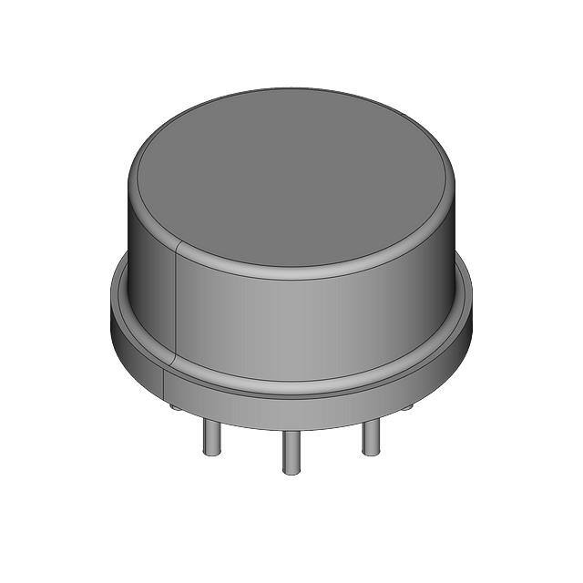
Connection Diagrams
Note: Pin 4 connected to case
Figure 1. Metal Can Package
Top View
See Package Number LMC0008C
Figure 2. Dual-In-Line Package
Top View
See Package Number NAB0008A
Figure 3. Dual-In-Line Package
Top View
See Package Number J0014A
1
2
Please be aware that an important notice concerning availability, standard warranty, and use in critical applications of
Texas Instruments semiconductor products and disclaimers thereto appears at the end of this data sheet.
All trademarks are the property of their respective owners.
PRODUCTION DATA information is current as of publication date.
Products conform to specifications per the terms of the Texas
Instruments standard warranty. Production processing does not
necessarily include testing of all parameters.
Copyright © 2008–2013, Texas Instruments Incorporated
�LM111JAN
SNOSAM9B – JULY 2008 – REVISED MARCH 2013
www.ti.com
Figure 4. See Package Number NAD0010A, NAC0010A
Schematic Diagram
Note: Pin connections shown on schematic diagram are for LMC0008C package.
These devices have limited built-in ESD protection. The leads should be shorted together or the device placed in conductive foam
during storage or handling to prevent electrostatic damage to the MOS gates.
2
Submit Documentation Feedback
Copyright © 2008–2013, Texas Instruments Incorporated
Product Folder Links: LM111JAN
�LM111JAN
www.ti.com
SNOSAM9B – JULY 2008 – REVISED MARCH 2013
Absolute Maximum Ratings (1)
Positive Supply Voltage
+30.0V
Negative Supply Voltage
-30.0V
Total Supply Voltage
36V
Output to Negative Supply Voltage
50V
GND to Negative Supply Voltage
30V
Differential Input Voltage
±30V
Sink Current
50mA
Input Voltage
(2)
±15V
Power Dissipation (3)
8 LD CERDIP
400mW @ 25°C
8 LD Metal Can
330mW @ 25°C
10 LD CERPACK
330mW @ 25°C
10 LD Ceramic SOIC
330mW @ 25°C
14 LD CERDIP
400mW @ 25°C
Output Short Circuit Duration
10 seconds
Maximum Strobe Current
10mA
-55°C ≤ TA ≤ 125°C
Operating Temperature Range
Thermal Resistance
θJA
θJC
8 LD CERDIP (Still Air @ 0.5W)
120°C/W
8 LD CERDIP (500LF/Min Air flow @ 0.5W)
76°C/W
8 LD Metal Can (Still Air @ 0.5W)
150°C/W
8 LD Metal Can (500LF/Min Air flow @ 0.5W)
92°C/W
10 Ceramic SOIC (Still Air @ 0.5W)
231°C/W
10 Ceramic SOIC (500LF/Min Air flow @ 0.5W)
153°C/W
10 CERPACK (Still Air @ 0.5W)
231°C/W
10 CERPACK (500LF/Min Air flow @ 0.5W)
153°C/W
14 LD CERDIP (Still Air @ 0.5W)
120°C/W
14 LD CERDIP (500LF/Min Air flow @ 0.5W)
65°C/W
8 LD CERDIP
35°C/W
8 LD Metal Can Pkg
40°C/W
10 LD Ceramic SOIC
60°C/W
10 LD CERPACK
60°C/W
14 LD CERDIP
35°C/W
-65°C ≤ TA ≤ 150°C
Storage Temperature Range
Maximum Junction Temperature
175°C
Lead Temperature (Soldering, 60 seconds)
300°C
Voltage at Strobe Pin
V+ -5V
Package Weight (Typical)
8 LD Metal Can
965mg
8 LD CERDIP
1100mg
10 LD CERPACK
250mg
10 LD Ceramic SOIC
225mg
14 LD CERDIP
ESD Rating
(1)
(2)
(3)
(4)
(4)
TBD
300V
Absolute Maximum Ratings indicate limits beyond which damage to the device may occur. Operating Ratings indicate conditions for
which the device is functional, but do not ensure specific performance limits. For ensured specifications and test conditions, see the
Electrical Characteristics. The ensured specifications apply only for the test conditions listed. Some performance characteristics may
degrade when the device is not operated under the listed test conditions.
This rating applies for ±15V supplies. The positive input voltage limit is 30 V above the negative supply. The negative input voltage limit
is equal to the negative supply voltage or 30V below the positive supply, whichever is less.
The maximum power dissipation must be derated at elevated temperatures and is dictated by TJmax (maximum junction temperature),
θJA (package junction to ambient thermal resistance), and TA (ambient temperature). The maximum allowable power dissipation at any
temperature is PDmax = (TJmax - TA)/θJA or the number given in the Absolute Maximum Ratings, whichever is lower.
Human body model, 1.5 kΩ in series with 100 pF.
Submit Documentation Feedback
Copyright © 2008–2013, Texas Instruments Incorporated
Product Folder Links: LM111JAN
3
�LM111JAN
SNOSAM9B – JULY 2008 – REVISED MARCH 2013
www.ti.com
Recommended Operating Conditions
Supply Voltage
VCC = ±15VDC
-55°C ≤ TA ≤ 125°C
Operating Temperature Range
Quality Conformance Inspection
Mil-Std-883, Method 5005 — Group A
Subgroup
Description
Temperature (°C)
1
Static tests at
+25
2
Static tests at
+125
3
Static tests at
-55
4
Dynamic tests at
+25
5
Dynamic tests at
+125
6
Dynamic tests at
-55
7
Functional tests at
+25
8A
Functional tests at
+125
8B
Functional tests at
-55
9
Switching tests at
+25
10
Switching tests at
+125
11
Switching tests at
-55
LM111 JAN Electrical Characteristics DC Parameters
The following conditions apply, unless otherwise specified.
DC:
VCC = ±15V, VCM = 0
Symbol
VIO
Input Offset Voltage
VIO R
IIO
(1)
4
Parameter
Raised Input Offset Voltage
Input Offset Current
Min
Max
Unit
Subgroups
-3.0
+3.0
mV
1
-4.0
+4.0
mV
2, 3
+VCC = 29.5V, -VCC = -0.5V,
VI = 0V, VCM = -14.5V,
RS = 50Ω
-3.0
+3.0
mV
1
-4.0
+4.0
mV
2, 3
+VCC = 2V, -VCC = -28V,
VI = 0V, VCM = +13V,
RS = 50Ω
-3.0
+3.0
mV
1
-4.0
+4.0
mV
2, 3
+VCC = +2.5V, -VCC = -2.5V,
VI = 0V, RS = 50Ω
-3.0
+3.0
mV
1
-4.0
+4.0
mV
2, 3
-3.0
+3.0
mV
1
-4.5
+4.5
mV
2, 3
-3.0
+3.0
mV
1
-4.5
+4.5
mV
2, 3
-3.0
+3.0
mV
1
-4.5
+4.5
mV
2, 3
-10
+10
nA
1, 2
-20
+20
nA
3
+VCC = 29.5V, -VCC = -0.5V,
VI = 0V, VCM = -14.5V,
RS = 50KΩ
-10
+10
nA
1, 2
-20
+20
nA
3
+VCC = 2V, -VCC = -28V,
VI = 0V, VCM = +13V,
RS = 50KΩ
-10
+10
nA
1, 2
-20
+20
nA
3
Conditions
Notes
VI = 0V, RS = 50Ω
VI = 0V, RS = 50Ω
See (1)
+VCC = 29.5V, -VCC = -0.5V,
VI = 0V, VCM = -14.5V,
RS = 50Ω
See (1)
+VCC = 2V, -VCC = -28V,
VI = 0V, VCM = +13V,
RS = 50Ω
See (1)
VI = 0V, RS = 50KΩ
Subscript (R) indicates tests which are performed with input stage current raised by connecting BAL and BAL/STB terminals to +VCC.
Submit Documentation Feedback
Copyright © 2008–2013, Texas Instruments Incorporated
Product Folder Links: LM111JAN
�LM111JAN
www.ti.com
SNOSAM9B – JULY 2008 – REVISED MARCH 2013
LM111 JAN Electrical Characteristics DC Parameters (continued)
The following conditions apply, unless otherwise specified.
DC:
VCC = ±15V, VCM = 0
Symbol
IIOR
Raised Input Offset Current
±IIB
Min
Max
Unit
Subgroups
-25
+25
nA
1, 2
-50
+50
nA
3
-100
0.1
nA
1, 2
-150
0.1
nA
3
+VCC = 29.5V, -VCC = -0.5V,
VI = 0V, VCM = -14.5V,
RS = 50KΩ
-150
0.1
nA
1, 2
-200
0.1
nA
3
+VCC = 2V, -VCC = -28V,
VI = 0V, VCM = +13V,
RS = 50KΩ
-150
0.1
nA
1, 2
-200
0.1
nA
3
14
V
1, 2, 3
80
dB
1, 2, 3
Parameter
Input Bias Current
Conditions
VI = 0V, RS = 50KΩ
Collector Output Voltage (Strobe)
+VI = Gnd, -VI = 15V,
ISt = -3mA, RS = 50Ω
CMRR
Common Mode Rejection
-28V ≤ -VCC ≤ -0.5V, RS=50Ω, 2V ≤
+VCC ≤ 29.5V, RS = 50Ω, -14.5V ≤
VCM ≤ 13V,RS = 50Ω
Low Level Output Voltage
See (1)
VI = 0V, RS = 50KΩ
VOSt
VOL
Notes
See (2)
+VCC = 4.5V, -VCC = Gnd,
IO = 8mA, ±VI = 0.5V,
VID = -6mV
See (3)
0.4
V
1, 2, 3
+VCC = 4.5V, -VCC = Gnd,
IO = 8mA, ±VI = 3V,
VID = -6mV
See (3)
0.4
V
1, 2, 3
IO = 50mA, ±VI = 13V,
VID = -5mV
See (3)
1.5
V
1, 2, 3
IO = 50mA, ±VI = -14V,
VID = -5mV
See (3)
1.5
V
1, 2, 3
-1.0
10
nA
1
ICEX
Output Leakage Current
+VCC = 18V, -VCC = -18V,
VO = 32V
-1.0
500
nA
2
IIL
Input Leakage Current
+VCC = 18V, -VCC = -18V,
+VI = +12V, -VI = -17V
-5.0
500
nA
1, 2, 3
+VCC = 18V, -VCC = -18V,
+VI = -17V, -VI = +12V
-5.0
500
nA
1, 2, 3
6.0
mA
1, 2
7.0
mA
3
-5.0
mA
1, 2
-6.0
mA
3
+ICC
-ICC
Power Supply Current
Power Supply Current
Δ VIO / Δ T
Δ IIO / Δ T
IOS
Temperature Coefficient Input
Offset Voltage
25°C ≤ T ≤ 125°C
See (4)
-25
25
uV/°C
2
-55°C ≤ T ≤ 25°C
See
(4)
-25
25
uV/°C
3
Temperature Coefficient Input
Offset Current
25°C ≤ T ≤ 125°C
See (4)
-100
100
pA/°C
2
-55°C ≤ T ≤ 25°C
See (4)
-200
200
pA/°C
3
Short Circuit Current
VO = 5V, t ≤ 10mS, -VI = 0.1V,
+VI = 0V
200
mA
1
150
mA
2
250
mA
3
mV
1
+VIO adj.
Input Offset Voltage (Adjustment)
VO = 0V, VI = 0V, RS = 50Ω
-VIO adj.
Input Offset Voltage (Adjustment)
VO = 0V, VI = 0V, RS = 50Ω
±AVE
Voltage Gain (Emitter)
RL = 600Ω
(2)
(3)
(4)
(5)
5.0
mV
1
See (5)
10
-5.0
V/mV
4
See (5)
8.0
V/mV
5, 6
IST = −2mA at −55°C
VID is voltage difference between inputs.
Calculated parameter.
Datalog reading in K=V/mV.
Submit Documentation Feedback
Copyright © 2008–2013, Texas Instruments Incorporated
Product Folder Links: LM111JAN
5
�LM111JAN
SNOSAM9B – JULY 2008 – REVISED MARCH 2013
www.ti.com
LM111 JAN Electrical Characteristics AC Parameters
The following conditions apply, unless otherwise specified.
AC:
VCC = ±15V, VCM = 0
Symbol
tRLHC
tRHLC
Max
Unit
Subgroups
Response Time (Collector Output) VOD(Overdrive) = -5mV,
CL = 50pF, VI = -100mV
300
nS
7, 8B
640
nS
8A
Response Time (Collector Output) VOD(Overdrive) = 5mV,
CL = 50pF, VI = 100mV
300
nS
7, 8B
500
nS
8A
Min
Max
Unit
Subgroups
VI = 0V, RS = 50Ω
-0.5
0.5
mV
1
+VCC = 29.5V, -VCC = -0.5V,
VI = 0V, VCM = -14.5V,
RS = 50Ω
-0.5
0.5
mV
1
+VCC = 2V, -VCC = -28V,
VI = 0V, VCM = +13V,
RS = 50Ω
-0.5
0.5
mV
1
VI = 0V, RS = 50KΩ
-12.5
12.5
nA
1
+VCC = 29.5V, -VCC = -0.5V,
VI = 0V, VCM = -14.5V,
RS = 50KΩ
-12.5
12.5
nA
1
+VCC = 2V, -VCC = -28V,
VI = 0V, VCM = +13V,
RS = 50KΩ
-12.5
12.5
nA
1
+VCC = 18V, -VCC = -18V,
VO = 32V
-5.0
5.0
nA
1
Parameter
Conditions
Notes
Min
LM111 JAN Electrical Characteristics DC Drift Parameters
The following conditions apply, unless otherwise specified.
DC:
VCC = ±15V, VCM = 0
Delta calculations performed on JANS devices at group B , subgroup 5.
Symbol
VIO
±IIB
ICEX
6
Parameter
Input Offset Voltage
Input Bias Current
Output Leakage Current
Conditions
Submit Documentation Feedback
Notes
Copyright © 2008–2013, Texas Instruments Incorporated
Product Folder Links: LM111JAN
�LM111JAN
www.ti.com
SNOSAM9B – JULY 2008 – REVISED MARCH 2013
LM111 Typical Performance Characteristics
Input Bias Current
Input Bias Current
Figure 5.
Figure 6.
Input Bias Current
Input Bias Current
Figure 7.
Figure 8.
Input Bias Current
Input Bias Current
Figure 9.
Figure 10.
Submit Documentation Feedback
Copyright © 2008–2013, Texas Instruments Incorporated
Product Folder Links: LM111JAN
7
�LM111JAN
SNOSAM9B – JULY 2008 – REVISED MARCH 2013
www.ti.com
LM111 Typical Performance Characteristics (continued)
8
Input Bias Current
Input Overdrives
Input Bias Current
Input Overdrives
Figure 11.
Figure 12.
Input Bias Current
Response Time for Various
Input Overdrives
Figure 13.
Figure 14.
Response Time for Various
Input Overdrives
Output Limiting Characteristics
Figure 15.
Figure 16.
Submit Documentation Feedback
Copyright © 2008–2013, Texas Instruments Incorporated
Product Folder Links: LM111JAN
�LM111JAN
www.ti.com
SNOSAM9B – JULY 2008 – REVISED MARCH 2013
LM111 Typical Performance Characteristics (continued)
Supply Current
Supply Current
Figure 17.
Figure 18.
Leakage Currents
Figure 19.
Submit Documentation Feedback
Copyright © 2008–2013, Texas Instruments Incorporated
Product Folder Links: LM111JAN
9
�LM111JAN
SNOSAM9B – JULY 2008 – REVISED MARCH 2013
www.ti.com
APPLICATION HINTS
CIRCUIT TECHNIQUES FOR AVOIDING
OSCILLATIONS IN COMPARATOR APPLICATIONS
When a high-speed comparator such as the LM111 is used with fast input signals and low source impedances,
the output response will normally be fast and stable, assuming that the power supplies have been bypassed (with
0.1 μF disc capacitors), and that the output signal is routed well away from the inputs (pins 2 and 3) and also
away from pins 5 and 6.
However, when the input signal is a voltage ramp or a slow sine wave, or if the signal source impedance is high
(1 kΩ to 100 kΩ), the comparator may burst into oscillation near the crossing-point. This is due to the high gain
and wide bandwidth of comparators such as the LM111. To avoid oscillation or instability in such a usage,
several precautions are recommended, as shown in Figure 20 below.
1. The trim pins (pins 5 and 6) act as unwanted auxiliary inputs. If these pins are not connected to a trim-pot,
they should be shorted together. If they are connected to a trim-pot, a 0.01 μF capacitor C1 between pins 5
and 6 will minimize the susceptibility to AC coupling. A smaller capacitor is used if pin 5 is used for positive
feedback as in Figure 20.
2. Certain sources will produce a cleaner comparator output waveform if a 100 pF to 1000 pF capacitor C2 is
connected directly across the input pins.
3. When the signal source is applied through a resistive network, RS, it is usually advantageous to choose an
RS′ of substantially the same value, both for DC and for dynamic (AC) considerations. Carbon, tin-oxide, and
metal-film resistors have all been used successfully in comparator input circuitry. Inductive wire wound
resistors are not suitable.
4. When comparator circuits use input resistors (e.g. summing resistors), their value and placement are
particularly important. In all cases the body of the resistor should be close to the device or socket. In other
words there should be very little lead length or printed-circuit foil run between comparator and resistor to
radiate or pick up signals. The same applies to capacitors, pots, etc. For example, if RS=10 kΩ, as little as 5
inches of lead between the resistors and the input pins can result in oscillations that are very hard to damp.
Twisting these input leads tightly is the only (second best) alternative to placing resistors close to the
comparator.
5. Since feedback to almost any pin of a comparator can result in oscillation, the printed-circuit layout should be
engineered thoughtfully. Preferably there should be a ground plane under the LM111 circuitry, for example,
one side of a double-layer circuit card. Ground foil (or, positive supply or negative supply foil) should extend
between the output and the inputs, to act as a guard. The foil connections for the inputs should be as small
and compact as possible, and should be essentially surrounded by ground foil on all sides, to guard against
capacitive coupling from any high-level signals (such as the output). If pins 5 and 6 are not used, they should
be shorted together. If they are connected to a trim-pot, the trim-pot should be located, at most, a few inches
away from the LM111, and the 0.01 μF capacitor should be installed. If this capacitor cannot be used, a
shielding printed-circuit foil may be advisable between pins 6 and 7. The power supply bypass capacitors
should be located within a couple inches of the LM111. (Some other comparators require the power-supply
bypass to be located immediately adjacent to the comparator.)
6. It is a standard procedure to use hysteresis (positive feedback) around a comparator, to prevent oscillation,
and to avoid excessive noise on the output because the comparator is a good amplifier for its own noise. In
the circuit of Figure 21, the feedback from the output to the positive input will cause about 3 mV of
hysteresis. However, if RS is larger than 100Ω, such as 50 kΩ, it would not be reasonable to simply increase
the value of the positive feedback resistor above 510 kΩ. The circuit of Figure 22 could be used, but it is
rather awkward. See the notes in paragraph 7 below.
7. When both inputs of the LM111 are connected to active signals, or if a high-impedance signal is driving the
positive input of the LM111 so that positive feedback would be disruptive, the circuit of Figure 20 is ideal.
The positive feedback is to pin 5 (one of the offset adjustment pins). It is sufficient to cause 1 to 2 mV
hysteresis and sharp transitions with input triangle waves from a few Hz to hundreds of kHz. The positivefeedback signal across the 82Ω resistor swings 240 mV below the positive supply. This signal is centered
around the nominal voltage at pin 5, so this feedback does not add to the VOS of the comparator. As much as
8 mV of VOS can be trimmed out, using the 5 kΩ pot and 3 kΩ resistor as shown.
8. These application notes apply specifically to the LM111 and LF111 families of comparators, and are
applicable to all high-speed comparators in general, (with the exception that not all comparators have trim
pins).
10
Submit Documentation Feedback
Copyright © 2008–2013, Texas Instruments Incorporated
Product Folder Links: LM111JAN
�LM111JAN
www.ti.com
SNOSAM9B – JULY 2008 – REVISED MARCH 2013
Pin connections shown are for LM111H in the LMC0008C hermetic package
Figure 20. Improved Positive Feedback
Pin connections shown are for LM111H in the LMC0008C hermetic package
Figure 21. Conventional Positive Feedback
Submit Documentation Feedback
Copyright © 2008–2013, Texas Instruments Incorporated
Product Folder Links: LM111JAN
11
�LM111JAN
SNOSAM9B – JULY 2008 – REVISED MARCH 2013
www.ti.com
Figure 22. Positive Feedback with High Source Resistance
12
Submit Documentation Feedback
Copyright © 2008–2013, Texas Instruments Incorporated
Product Folder Links: LM111JAN
�LM111JAN
www.ti.com
SNOSAM9B – JULY 2008 – REVISED MARCH 2013
Typical Applications
Pin connections shown on schematic diagram and typical applications are for LMC0008C metal can package.
Offset Balancing
Strobing
Note: Do Not Ground Strobe Pin. Output is turned off when current
is pulled from Strobe Pin.
Figure 23.
Figure 24.
Increasing Input Stage Current
Detector for Magnetic Transducer
Note: Increases typical common mode slew from 7.0V/μs to 18V/μs.
Figure 25.
Figure 26.
Digital Transmission Isolator
Relay Driver with Strobe
*Absorbs inductive kickback of relay and protects IC from severe
voltage transients on V++ line.
Note: Do Not Ground Strobe Pin.
Figure 27.
Figure 28.
Submit Documentation Feedback
Copyright © 2008–2013, Texas Instruments Incorporated
Product Folder Links: LM111JAN
13
�LM111JAN
SNOSAM9B – JULY 2008 – REVISED MARCH 2013
www.ti.com
Strobing off Both Input and Output Stages
Note:Typical input current is 50 pA with inputs strobed off.
Figure 29.
Positive Peak Detector
Zero Crossing Detector Driving MOS Logic
*Solid tantalum
Figure 30.
Figure 31.
Typical Applications
(Pin numbers refer to LMC0008C package)
Zero Crossing Detector Driving MOS Switch
100 kHz Free Running Multivibrator
*TTL or DTL fanout of two
Figure 32.
14
Figure 33.
Submit Documentation Feedback
Copyright © 2008–2013, Texas Instruments Incorporated
Product Folder Links: LM111JAN
�LM111JAN
www.ti.com
SNOSAM9B – JULY 2008 – REVISED MARCH 2013
10 Hz to 10 kHz Voltage Controlled Oscillator
*Adjust for symmetrical square wave time when VIN = 5 mV
†Minimum capacitance 20 pF Maximum frequency 50 kHz
Figure 34.
Driving Ground-Referred Load
Using Clamp Diodes to Improve Response
*Input polarity is reversed when using pin 1 as output.
Figure 35.
Figure 36.
TTL Interface with High Level Logic
*Values shown are for a 0 to 30V logic swing and a 15V threshold.
†May be added to control speed and reduce susceptibility to noise spikes.
Figure 37.
Submit Documentation Feedback
Copyright © 2008–2013, Texas Instruments Incorporated
Product Folder Links: LM111JAN
15
�LM111JAN
SNOSAM9B – JULY 2008 – REVISED MARCH 2013
www.ti.com
Crystal Oscillator
Comparator and Solenoid Driver
Figure 38.
Precision Squarer
*Solid tantalum
†Adjust to set clamp level
Figure 39.
Low Voltage Adjustable Reference Supply
*Solid tantalum
Figure 40.
Positive Peak Detector
Figure 41.
Zero Crossing Detector Driving MOS Logic
*Solid tantalum
Figure 42.
16
Figure 43.
Submit Documentation Feedback
Copyright © 2008–2013, Texas Instruments Incorporated
Product Folder Links: LM111JAN
�LM111JAN
www.ti.com
SNOSAM9B – JULY 2008 – REVISED MARCH 2013
Negative Peak Detector
Precision Photodiode Comparator
*Solid tantalum
*R2 sets the comparison level. At comparison, the photodiode has
less than 5 mV across it, decreasing leakages by an order of
magnitude.
Figure 44.
Figure 45.
Switching Power Amplifier
Switching Power Amplifier
Figure 46.
Figure 47.
Submit Documentation Feedback
Copyright © 2008–2013, Texas Instruments Incorporated
Product Folder Links: LM111JAN
17
�LM111JAN
SNOSAM9B – JULY 2008 – REVISED MARCH 2013
www.ti.com
REVISION HISTORY SECTION
Released
Revision
Section
05/09/05
A
New Release, Corporate
format
03/26/2013
B
All Sections
18
Originator
L. Lytle
Submit Documentation Feedback
Changes
1 MDS data sheets converted into one Corp.
data sheet format. MJLM111–X Rev 0D3 will
be archived.
Changed layout of National Data Sheet to TI
format
Copyright © 2008–2013, Texas Instruments Incorporated
Product Folder Links: LM111JAN
�PACKAGE OPTION ADDENDUM
www.ti.com
10-Dec-2020
PACKAGING INFORMATION
Orderable Device
Status
(1)
Package Type Package Pins Package
Drawing
Qty
Eco Plan
(2)
Lead finish/
Ball material
MSL Peak Temp
Op Temp (°C)
(3)
Device Marking
(4/5)
(6)
JL111BGA
ACTIVE
TO-99
LMC
8
20
Non-RoHS &
Non-Green
Call TI
Call TI
-55 to 125
JL111BGA
JM38510/10304BGA Q
ACO
JM38510/10304BGA Q
>T
JM38510/10304BGA
ACTIVE
TO-99
LMC
8
20
Non-RoHS &
Non-Green
Call TI
Call TI
-55 to 125
JL111BGA
JM38510/10304BGA Q
ACO
JM38510/10304BGA Q
>T
M38510/10304BGA
ACTIVE
TO-99
LMC
8
20
Non-RoHS &
Non-Green
Call TI
Call TI
-55 to 125
JL111BGA
JM38510/10304BGA Q
ACO
JM38510/10304BGA Q
>T
(1)
The marketing status values are defined as follows:
ACTIVE: Product device recommended for new designs.
LIFEBUY: TI has announced that the device will be discontinued, and a lifetime-buy period is in effect.
NRND: Not recommended for new designs. Device is in production to support existing customers, but TI does not recommend using this part in a new design.
PREVIEW: Device has been announced but is not in production. Samples may or may not be available.
OBSOLETE: TI has discontinued the production of the device.
(2)
RoHS: TI defines "RoHS" to mean semiconductor products that are compliant with the current EU RoHS requirements for all 10 RoHS substances, including the requirement that RoHS substance
do not exceed 0.1% by weight in homogeneous materials. Where designed to be soldered at high temperatures, "RoHS" products are suitable for use in specified lead-free processes. TI may
reference these types of products as "Pb-Free".
RoHS Exempt: TI defines "RoHS Exempt" to mean products that contain lead but are compliant with EU RoHS pursuant to a specific EU RoHS exemption.
Green: TI defines "Green" to mean the content of Chlorine (Cl) and Bromine (Br) based flame retardants meet JS709B low halogen requirements of