LT1031/LH0070
Precision 10V Reference
U
FEATURES
■
■
■
■
■
■
■
■
DESCRIPTIO
The LT ®1031 is a precision 10V reference with ultralow
drift and noise, extremely good long term stability, and
almost total immunity to input voltage variations. The
reference output will both source and sink up to 10mA and
can be used as a shunt regulator (two terminal Zener) with
the same precision characteristics as the three terminal
connection. Special care has been taken to minimize
thermal regulation effects and temperature induced
hysteresis.
Pin Compatible with LH0070 and AD581*
Ultralow Drift—5ppm/°C Max Slope
Trimmed Output Voltage
Operates in Series or Shunt Mode
Output Sinks and Sources in Series Mode
Very Low Noise < 1ppmP-P 0.1Hz to 10Hz
> 100dB Ripple Rejection
Minimum Input Voltage of 11V
U
APPLICATIO S
■
■
■
■
■
■
The LT1031 reference is based on a buried Zener diode
structure which eliminates noise and stability problems
associated with surface breakdown devices. Further, a
subsurface Zener exhibits better temperature drift and
time stability than even the best band-gap references.
A-to-D and D-to-A Converters
Precision Regulators
Digital Voltmeters
lnertial Navigation Systems
Precision Scales
Portable Reference Standard
Unique circuit design makes the LT1031 the first three
terminal IC reference to offer ultralow drift without the
use of high power on-chip heaters. Output voltage is
pretrimmed to 0.05% accuracy.
The LT1031 can be used as a plug-in replacement for
the AD581 and LH0070,* with improved electrical and
thermal performance.
, LTC and LT are registered trademarks of Linear Technology Corporation.
All other trademarks are the property of their respective owners.
*See LH0070 Electrical Characteristics table and AD581 cross reference guide.
U
TYPICAL APPLICATIO
Basic Positive and
Negative Connections
IN
TA = 25°C
35 DISTRIBUTION
FROM 5 RUNS
LT1031
OUT
VOUT
OUT
GND
GND
– VOUT
R1 =
VIN – VOUT
ILOAD + 1.5mA
PERCENT OF UNITS (%)
LT1031
VIN
Distribution of Output Accuracy
40
30
25
20
15
10
R1
5
– VIN
LT1031 • TA01
0
–0.10 –0.06
–0.02 0 0.02
0.06
OUTPUT ACCURACY (%)
0.10
LT1031 TA02
1031fb
1
�LT1031/LH0070
W W
W
AXI U
U
ABSOLUTE
RATI GS
U
U
W
PACKAGE/ORDER I FOR ATIO
(Note 1)
Input Voltage ........................................................... 40V
Input-Output Voltage Differential ............................. 35V
Output to Ground Voltage
(Shunt Mode Current Limit) ................................. 16V
Trim Pin to Ground Voltage
Positive ................................................. Equal to VOUT
Negative ............................................................. –20V
Output Short-Circuit Duration
VIN = 35V ......................................................... 10 sec
VIN ≤ 20V ..................................................... Indefinite
Operating Temperature Range
LT1031M .......................................... –55°C to 125°C
LT1031C .................................................. 0°C to 70°C
Lead Temperature (Soldering, 10 sec).................. 300°C
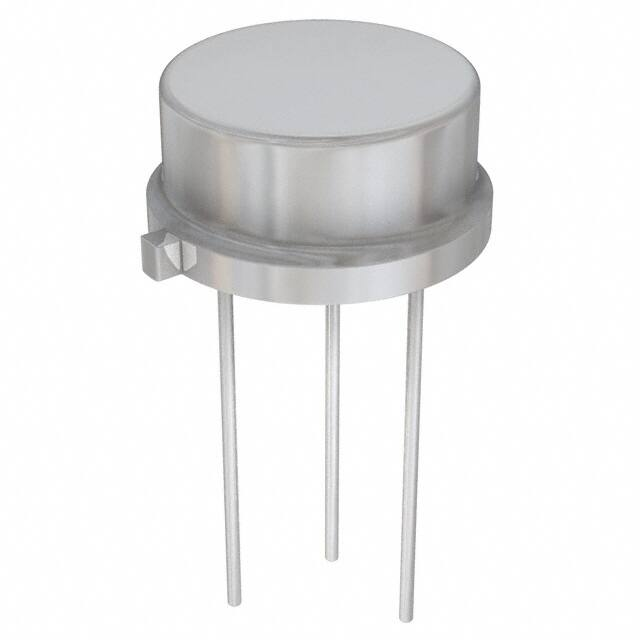
BOTTOM VIEW
INPUT
1
2
OUTPUT
3
GROUND
H PACKAGE
3-LEAD TO-39 METAL CAN
TJMAX = 150°C, θJA = 150°C/W, θJC = 45°C/W (LH0070)
TJMAX = 150°C, θJA = 150°C/W, θJC = 45°C/W (LT1031M)
TJMAX = 85°C, θJA = 150°C/W, θJC = 45°C/W (LT1031C)
ORDER PART NUMBER
LH0070-0H
LH0070-1H
LH0070-2H
LT1031BMH
LT1031DMH
LT1031BCH
LT1031CCH
LT1031DCH
ELECTRICAL CHARACTERISTICS
(LT1031) The ● denotes the specifications which apply over the full operating
temperature range, otherwise specifications are at TA = 25°C. VIN = 15V, IOUT = 0, Mil or Comm version, unless noted.
SYMBOL
PARAMETER
CONDITIONS
MIN
LT1031
TYP
MAX
VR
Output Voltage (Note 2)
LT1031B
LT1031C
LT1031D
9.995
9.990
9.980
10.000
10.000
10.000
10.005
10.010
10.020
∆VR
∆T
Output Voltage Temperature
Coefficient (Note 3)
TMIN ≤ TJ ≤ TMAX
LT1031B
LT1031C
LT1031D
3
6
10
5
15
25
ppm/°C
ppm/°C
ppm/°C
∆VR
∆VIN
Line Regulation (Note 4)
11.5V ≤ VIN ≤ 14.5V
1
4
6
ppm/V
ppm/V
0.5
2
4
ppm/V
ppm/V
12
25
40
ppm/mA
ppm/mA
50
100
150
ppm/mA
ppm/mA
1.2
1.7
2.0
mA
mA
1.1
1.5
mA
4.5V ≤ VIN ≤ 40V
●
●
●
●
●
0 ≤ IOUT ≤ 10mA
(Note 4)
●
1.7mA ≤ ISHUNT ≤ 10mA
(Notes 4, 5)
●
UNITS
V
V
V
∆VR
∆IO
Load Regulation (Sourcing Current)
∆VR
∆IO
Load Regulation (Shunt Mode)
IQ
Series Mode Supply Current
IMIN
Shunt Mode Minimum Current
VIN is Open
Output Short-Circuit Current
11V ≤ VIN ≤ 35V
Minimum Input Voltage (Note 7)
lOUT ≤ 1mA
en
Output Voltage Noise
0.1Hz ≤ f ≤ 10Hz
10Hz ≤ f ≤ 10kHz
6
11
µVP-P
µVRMS
∆VR
∆Time
Long Term Stability of
Output Voltage
∆t = 1000 Hrs
Non-Cumulative
15
ppm
Temperature Hysteresis of Output
∆T = 50°C
5
●
30
10.8
mA
11.0
V
ppm
1031fb
2
�LT1031/LH0070
ELECTRICAL CHARACTERISTICS
(LH0070) The ● denotes the specifications which apply over the full
operating temperature range. VIN = 15V, RL = 10kΩ, – 55°C ≤ TA ≤ 125°C, unless noted.
SYMBOL
PARAMETER
CONDITIONS
VR
Output Voltage
TA = 25°C
∆VR
Output Accuracy
– 0, –1
–2
TA = 25°C
Output Accuracy
– 0, –1
–2
TA = –55°C, 125°C
Output Voltage Change
with Temperature
–0
–1
–2
Note 6
Line Regulation
– 0, –1
–2
13V ≤ VIN ≤ 33V, TA = 25°C
∆VR
∆VR
∆T
∆VR
∆VIN
MIN
LH0070
TYP
MAX
10.000
± 0.03
± 0.02
●
Input Voltage Range
V
± 0.1
± 0.05
%
%
0.3
0.2
%
%
± 0.02
± 0.01
± 0.2
± 0.1
± 0.04
%
%
%
0.006
0.006
0.1
0.03
%
%
40
V
●
●
●
●
UNITS
11.4
∆VR
∆IO
Load Regulation
0mA ≤ lOUT ≤ 5mA
●
0.01
0.03
%
IQ
Quiescent Current
13V ≤ VIN ≤ 33V
●
1.2
5
mA
∆lQ
∆VIN
Change in Quiescent Current
∆VIN = 20V from 13V TO 33V
●
0.1
1.5
mA
en
Output Noise Voltage
Ripple Rejection
rO
Output Resistance
∆VZ
∆Time
Long Term Stability
– 0, –1
–2
f = 120Hz
TA = 25°C (Note 8)
Note 1: Absolute Maximum Ratings are those values beyond which the life
of a device may be impaired.
Note 2: Output voltage is measured immediately after turn-on. Changes
due to chip warm-up are typically less than 0.005%.
Note 3: Temperature coefficient is measured by dividing the change in
output voltage over the temperature range by the change in temperature.
Separate tests are done for hot and cold: TMIN to 25°C and 25°C to TMAX.
Incremental slope is also measured at 25°C. For LT1031BMH, the
5ppm/°C drift specification is for – 25°C to 85°C. Drift over the full – 55°C
to 125°C range is guaranteed to 7ppm/°C.
6
µVP-P
●
0.001
%/VP-P
●
0.2
0.6
± 0.2
± 0.05
Ω
%/Yr
%/Yr
Note 4: Line and load regulation are measured on a pulse basis. Output
changes due to die temperature change must be taken into account
separately. Package thermal resistance is 150°C/W.
Note 5: Shunt mode regulation is measured with the input open. With the
input connected, shunt mode current can be reduced to 0mA. Load
regulation will remain the same.
Note 6: Temperature drift is guaranteed from –25°C to 85°C on LH0070.
Note 7: See curve for guaranteed minimum VIN versus IOUT.
Note 8: Guaranteed by design.
1031fb
3
�LT1031/LH0070
U
CROSS REFERENCE
The following cross reference guide may be used to select
LT1031 grades which meet or exceed output voltage,
temperature drift, load and line regulation, and output
current specifications of the AD581 reference. Parameters
such as noise, hysteresis, and long term stability will be
significantly better for all LT1031 grades compared to the
AD581.
CROSS REFERENCE GUIDE/LT1031 TO AD581
AD581J
order LT1031DCH
AD581K
order LT1031CCH
AD581L
order LT1031BCH
A0581S
order LT1031DMH
A0581U
order LT1031BMH
U W
TYPICAL PERFOR A CE CHARACTERISTICS
Ripple Rejection
115
Ripple Rejection
130
f = 150Hz
VIN = 15V
COUT = 0
120
110
Minimum Input Voltage
11.6
95
90
INPUT VOLTAGE (V)
REJECTION (dB)
REJECTION (dB)
100
100
90
80
0
5
10
15 20 25 30
INPUT VOLTAGE (V)
35
10.8
10.6
10.4
60
10.2
40
TJ = 25°C
11.0
70
10.0
50
85
TJ = –55°C
11.2
110
105
TJ = 125°C
GUARANTEED
CURVE-ALL
TEMPS
11.4
10
100
1k
FREQUENCY (Hz)
10k
0
2
4
6 8 10 12 14 16 18 20
OUTPUT CURRENT (mA)
LT1031 • TPC02
LT1031 • TPC01
LT1031 • TPC03
Start-Up (Series Mode)
12
Start-Up (Shunt Mode)
VIN = 0 TO 12V
400
350
10
OUTPUT VOLTAGE (V)
11
OUTPUT VOLTAGE (V)
Output Voltage Noise Spectrum
11
10
9
8
7
6
9
8
–12V
1k
VOUT
0V
7
OUT
NC
5
NOISE VOLTAGE (nV/√Hz)
13
IN
5
2
4
6
8
TIME (µs)
10
12
14
LT1031 • TPC04
200
150
100
50
4
0
250
GND
6
3
300
0
2
6
4
TIME (µs)
8
10
12
LT1031 • TPC05
0
10
100
1k
FREQUENCY (Hz)
10k
LT1031 • TPC06
1031fb
4
�LT1031/LH0070
U W
TYPICAL PERFOR A CE CHARACTERISTICS
Output Voltage Noise
Load Regulation
5
COUT = 0
FILTER = 1 POLE
fLOW = 0.1Hz
14
VIN = 12V
4
10.004
3
OUTPUT CHANGE (mV)
12
RMS NOISE (µV)
Output Voltage Temperature
10.006
10
8
6
4
OUTPUT VOLTAGE (V)
16
2
1
0
–1
–2
–3
2
10.002
10.000
9.998
9.996
–4
–5
–10 –8 –6 –4 –2 0 2 4 6 8
SOURCING
SINKING
OUTPUT CURRENT (mA)
0
10
100
1k
BANDWIDTH (Hz)
10k
LT1031 • TPC07
10
9.994
–50 –25
50
25
75
0
TEMPERATURE (˚C)
100
LT1031 • TPC09
LT1031 • TPC08
Input Supply Current
1.8
TJ = –55°C
60
INPUT PIN OPEN
1.6
TJ = 25°C
1.2
Shunt Mode Current Limit
TJ = 125°C
1.0
0.8
0.6
0.4
CURRENT INTO OUTPUT (mA)
IOUT = 0
1.4
1.4
TJ = –55°C
1.2
1.0
TJ = 25°C
0.8
0.6
0.4
TJ = 125°C
40
30
20
10
0.2
0.2
0
0
0
5
10
15
20
35
25 30
INPUT VOLTAGE (V)
0
2
4
6
10
8
OUTPUT TO GROUND VOLTAGE (V)
0
40
∆ISOURCE = 100µAp-p
VIN = 30V
∆POWER = 200mW
LOAD
REGULATION
THERMAL*
REGULATION
–1.5
ILOAD = 10mA
OUTPUT VOLTAGE CHANGE
ISOURCE = 0
0
–1.0
40 60 80 100 120 140
TIME (ms)
*INDEPENDENT OF TEMPERATURE COEFFICIENT
0
20
LT1031 • TPC13
2
4
6
8 10 12 14
OUTPUT VOLTAGE (V)
∆ISOURCE = 100µAp-p
ISOURCE = 0
ISINK = 0.8mA
–2
0
1
ISINK = 1.0mA
∆ISINK = 100µAp-p
ISINK = 0.8mA
20mV
5mV
ISINK = 1.2mA
ISOURCE = 0.5mA
ISOURCE = 2 TO 10mA
ISINK = 1.4mA
ISINK = 2 TO 10mA
ISINK = 2 TO 10mA
3 4 5 6 7 8
TIME (µs)
NOTE VERTICAL SCALE CHANGE
BETWEEN SOURCING AND SINKING
2
18
LT1031 • TPC12
∆ISINK = 100µAp-p
ISINK = 0.6mA
10mV
ISOURCE = 0.2mA
16
Load Transient Response
CLOAD = 1000pF
50mV
ISOURCE = 2 TO 10mA
–20
0
Load Transient Response
CLOAD = 0
Thermal Regulation
–0.5
12
LT1031 • TPC11
LT1031 • TPC10
OUTPUT CHANGE (mV)
INPUT PIN IS OPEN
50
OUTPUT VOLTAGE CHANGE
INPUT CURRENT (mA)
Shunt Characteristics
CURRENT INTO OUTPUT (mA)
1.8
1.6
125
9
LT1031 • TPC14
0
2
6 8 0 2 4 6
TIME (µs)
NOTE VERTICAL SCALE CHANGE
BETWEEN SOURCING AND SINKING
4
8
LT1031 • TPC15
1031fb
5
�LT1031/LH0070
U W
TYPICAL PERFOR A CE CHARACTERISTICS
Output Noise 0.1Hz to 10Hz
OUTPUT VOLTAGE NOISE (10µV/DIV)
FILTERING = 1 ZERO AT 0.1Hz
2 POLES AT 10Hz
10µV (1ppm)
0
1
4
3
2
TIME (MINUTES)
5
6
LT1031 • TPC16
U
W
U U
APPLICATIO S I FOR ATIO
Trimming Output Voltage
Effect of Reference Drift on System Accuracy
The LT1031 output can be trimmed by driving the ground
pin. The suggested method is shown in the illustration
below. A 5Ω resistor is inserted in series with the ground
pin. The top of the resistor is supplied current from a trim
potentiometer. This technique requires fairly high trim
current of up to 1.5mA from the LT1031 or 3.5mA from the
–15V supply; however it is necessary to maintain low drift
in the reference. Ground pin current changes in the LT1031,
with temperature, could be as high as 4µA/°C. This,
coupled with the 5Ω external resistor, creates up
to 2ppm/°C drift in the reference (5Ω • 4µA/°C = 20µV/°C
= 2ppm/°C). If induced drift higher than this can be
tolerated, all resistor values in the trim circuit can be raised
proportionately to reduce current drain.
A large portion of the temperature drift error budget in
many systems is the system reference voltage. The graph
below indicates the maximum temperature coefficient
allowable if the reference is to contribute no more than
1/2LSB error to the overall system performance. The
example shown is a 12-bit system designed to operate
over a temperature range from 25°C to 65°C. Assuming
the system calibration is performed at 25°C, the
temperature span is 40°C. The graph shows that the
temperature coefficient of the reference must be no worse
than 3ppm/°C if it is to contribute less than 1/2LSB error.
For this reason, the LT1031 has been optimized for low
drift.
LT1031
VIN
IN
OUT
VOUT
GND
R2*
4.3k
R3
50k
R1**
5Ω
–15V
*CAN BE INCREASED TO 5.6k FOR
LT1031B AND LH0070-2
**INCREASE TO 10Ω FOR LT1031D
LT1031 • TA04
MAXIMUM TEMPERATURE COEFFICIENT FOR
1/2LSB ERROR (ppm/°C)
Output Voltage Trimming
Maximum Allowable Reference Drift
100
8-BIT
10-BIT
10
12-BIT
14-BIT
1.0
10 20 30 40 50 60 70 80 90 100
TEMPERATURE SPAN (°C)
LT1031 • TA03
1031fb
6
�LT1031/LH0070
U
W
U U
APPLICATIO S I FOR ATIO
Series Mode with Boost Transistor
Capacitive Loading and Transient Response
The LT1031 is stable with all capacitive loads, but for
optimum settling with load transients, output capacitance
should be under 1000pF. The output stage of the reference
is class AB with a fairly low idling current. This makes
transient response worst-case at light load currents.
Because of internal current drain on the output, actual
worst-case occurs at I LOAD = 1.4mA (sinking).
Significantly better load transient response is obtained by
moving slightly away from these points. See Load
Transient Response curves for details. In general, best
transient response is obtained when the output is sourcing
current. In critical applications, a 10µF solid tantalum
capacitor with several ohms in series provides optimum
output bypass.
Kelvin Connections
The following circuits show proper hook-up to minimize
errors due to ground loops and line losses. Losses in the
output lead can be greatly reduced by adding a PNP boost
transistor if load currents are 5mA or higher. R2 can be
added to further reduce current in the output sense lead.
Standard Series Mode
LT1031
IN
OUT
R1
220Ω
2N3906
IN
LT1031
GND
OUT
R2*
5.6k
LOAD
GROUND
RETURN
*OPTIONAL—REDUCES CURRENT IN OUTPUT SENSE LEAD
LT1031 • TA06
Effects of Air Movement on Low Frequency Noise
Although the LT1031 does not have true force/sense
capability at its outputs, significant improvements in ground
loop and line loss problems can be achieved with proper
hook-up. In series mode operation, the ground pin of the
LT1031 carries only ≈1mA and can be used as a sense line,
greatly reducing ground loop and loss problems on the low
side of the reference. The high side supplies load current
so line resistance must be kept low. Twelve feet of
#22 gauge hook up wire or 1 foot of 0.025 inch printed
circuit trace will create 2mV loss at 10mA output current.
This is equivalent to 1LSB in a 10V, 12-bit system.
INPUT
INPUT
KEEP THIS LINE RESISTANCE LOW
+
GND
LOAD
GROUND
RETURN
LT1031 • TA05
The LT1031 has very low noise because of the buried zener
used in its design. In the 0.1Hz to 10Hz band, peak-to-peak
noise is about 0.5ppm of the DC output. To achieve this
low noise, however, care must be taken to shield the
reference from ambient air turbulence. Air movement can
create noise because of thermoelectric differences
between IC package leads (especially kovar lead TO-5) and
printed circuit board materials and/or sockets. Power
dissipation in the reference, even though it rarely exceeds
20mW, is enough to cause small temperature gradients in
the package leads. Variations in thermal resistance, caused
by uneven airflow, create differential lead temperatures,
thereby causing thermoelectric voltage noise at the output
of the reference. The XY plotter trace shown on the
following page dramatically illustrates this effect. The first
half of the plot was done with the LT1031 shielded from
ambient air with a small foam cup. The cup was then
removed for the second half of the trace. Ambient in both
cases was a lab environment with no excessive air turbulence from air conditioners, opening/closing doors, etc.
Removing the foam cup increases the output noise by
almost an order of magnitude in the 0.01Hz to 1Hz band!
The kovar leads of the TO-5 (H) package are the primary
culprit. Alloy 42 and copper lead frames used on dual-inline packages are not nearly as sensitive to thermally
generated noise because they are intrinsically matched.
1031fb
7
�LT1031/LH0070
U
W
U U
APPLICATIO S I FOR ATIO
(TO-5 PACKAGE)
f = 0.01Hz to 10Hz
OUTPUT VOLTAGE NOISE (20µV/DIV)
There is nothing magical about foam cups—any
enclosure which blocks air flow from the reference will do.
Smaller enclosures are better since they do not allow the
build-up of internally generated air movement. Naturally,
heat generating components external to the reference
itself should not be included inside the enclosure.
Noise Induced by Air Turbulence
(TO-5 Package)
20µV
0
FOAM CUP REMOVED
8
6
4
TIME (MINUTES)
2
10
12
LT1031 • TA07
U
APPLICATIO CIRCUITS
Negative Series Reference
Boosted Output Current with No Current Limit
V+ ≥ 11.8V
15V
R1
4.7k
IN
R2
4.7k
R1
220Ω
LT1031
2N2905
OUT
D1
15V
IN
GND
LT1031
–15V
–10V
AT 50mA
Q1
2N2905
OUT
+
GND
LT1031 • AC01
10V
AT 100mA
2µF
SOLID
TANT
LT1031 • AC02
Boosted Output Current with Current Limit
Handling Higher Load Currents
15V
V+ ≥ 12.8V
D1*
LED
R1
220Ω
8.2Ω
2N2905
GND
R1*
169Ω
IN
LT1031
VOUT = 10V
OUT
GND
IN
LT1031
30mA
RL
OUT
+
*GLOWS IN CURRENT LIMIT
DO NOT OMIT
10V
AT 100mA
2µF
SOLID
TANT
TYPICAL LOAD
CURRENT = 30mA
*SELECT R1 TO DELIVER TYPICAL LOAD CURRENT
LT1031 WILL THEN SOURCE OR SINK AS NECESSARY
TO MAINTAIN PROPER OUTPUT. DO NOT REMOVE LOAD,
AS OUTPUT WILL BE DRIVEN (UNREGULATED) HIGH. LINE
REGULATION IS DEGRADED IN THIS APPLICATION
LT1031 • AC04
LT1031 • AC03
1031fb
8
�LT1031/LH0070
U
APPLICATIO CIRCUITS
Strain Gauge Conditioner
for 350Ω Bridge
R1
357Ω
1/2W
28mA
LT1031
28.5mA
OUT
5V
350Ω STRAIN
GUAGE BRIDGE**
+
6
3
R2
20k
2
2
R4
20k
3
†
LM301A
1
100pF
–
R3
2MΩ
LT1012C
6
VOUT • 100
+
GND
–
IN
15V
R5
2M
8
R6
2MΩ*
–5V
357Ω
1/2W
–15V
*THIS RESISTOR PROVIDES POSITIVE FEEDBACK TO THE BRIDGE TO ELIMINATE
LOADING EFFECT OF THE AMPLIFIER. EFFECTIVE ZIN OF AMPLIFIER STAGE IS
≥ 1MΩ. IF R2–R5 ARE CHANGED, SET R6 = R3
**BRIDGE IS ULTRA LINEAR WHEN ALL LEGS ARE ACTIVE, TWO IN COMPRESSION
AND TWO IN TENSION, OR WHEN ONE SIDE IS ACTIVE WITH ONE COMPRESSED
AND ONE TENSIONED LEG
†
OFFSET AND DRIFT OF LM301A ARE VIRTUALLY ELIMINATED BY DIFERENTIAL
CONNECTION OF LT1012C
LT1031 • AC05
Ultralinear Platinum Temperature Sensor*
LT1031
OUT
IN
20V
GND
R2*
5k
R1**
253k
R9
100k
R14
5k
R10
182k
1%
R11
6.65M
1%
R15
10k
Rf**
654k
R8
10M
R12
1k
R4
4.75k
1%
R3**
5k
RS†
100Ω
AT 0°C
R7
392k
1%
–15V
R5
200k
1%
2
LT1001
3
R6
619k
1%
–
+
R13
24.3k
20V
7
6
VOUT = 100mV/°C
–50°C ≤ T ≤ 150°C
4
–15V
†
STANDARD INDUSTRIAL 100Ω PLATINUM 4-WIRE SENSOR, ROSEMOUNT 78S,
OR EQUIVALENT. α = 0.00385
TRIM R9 FOR VOUT = 0 AT 0°C
TRIM R12 FOR VOUT = 10V AT 100°C
TRIM R14 FOR VOUT = 5V AT 50°C
USE TRIM SEQUENCE AS SHOWN. TRIMS ARE NON-INTERACTIVE SO THAT ONLY ONE
TRIM SEQUENCE IS NORMALLY REQUIRED.
*FEEDBACK LINEARIZES OUTPUT TO ±0.005°C FROM – 50°C TO 150°C
**WIREWOUND RESISTORS WITH LOW TC
LT1031 • AC06
1031fb
9
�LT1031/LH0070
U
APPLICATIO CIRCUITS
2-Pole Lowpass Filtered Reference
MYLAR
1µF
VIN
–
R1
36k
LT1031
VIN
IN
LT1001
+
OUT
GND
+VREF
R2
36k
f = 10Hz
0.5µF
MYLAR
TOTAL NOISE
≤ 2µVRMS
1Hz ≤ f ≤ 10kHz
–VREF
LT1031 • AC07
Negative Shunt Reference Driven
by Current Source
LT1031
OUT
GND
–10V (ILOAD ≤ 1mA)
2.5mA
LM334
27Ω
–11V TO –40V
LT1031 • AC08
1031fb
10
�LT1031/LH0070
U
APPLICATIO CIRCUITS
Precision DAC Reference with System TC Trim
LT1031
15V
IN
OUT
8.87k
1%
GND
D1
IN457
50k
TC TRIM*
1.24k
1%
10k
1%
10k
1%
D2
IN457
50k
ROOM TEMP
TRIM
10.36k
1%
200k
1%
50k
8.45k
1mA
*TRIMS 1mA REFERENCE CURRENT
TC BY ± 40ppm/°C. THIS TRIM
SCHEME HAS VERY LITTLE EFFECT ON ROOM
TEMPERATURE CURRENT TO MINIMIZE ITERATIVE
TRIMMING.
DAC
LT1031 • AC09
W
U
EQUIVALENT SCHEMATIC
INPUT
Q3
D1
D2
OUTPUT
D3
R1
Q1
–
+
A1
R2
D4
6.3V
Q2
GND
LT1031 • ES01
1031fb
Information furnished by Linear Technology Corporation is believed to be accurate and reliable.
However, no responsibility is assumed for its use. Linear Technology Corporation makes no representation that the interconnection of its circuits as described herein will not infringe on existing patent rights.
11
�LT1031/LH0070
U
PACKAGE DESCRIPTIO
H Package
3-Lead TO-39 Metal Can
(Reference LTC DWG # 05-08-1330)
.350 – .370
(8.890 – 9.398)
.305 – .335
(7.747 – 8.509)
.050
(1.270)
MAX
.165 – .185
(4.191 – 4.699)
REFERENCE
PLANE
*
.016 – .019**
(0.406 – 0.483)
DIA
.500
(12.700)
MIN
.200
(5.080)
TYP
.100
(2.540)
PIN 1
.029 – .045
(0.737 – 1.143)
.100
(2.540)
.028 – .034
(0.711 – 0.864)
45°
H3(TO-39) 0801
*LEAD DIAMETER IS UNCONTROLLED BETWEEN THE REFERENCE PLANE
AND .050" BELOW THE REFERENCE PLANE
.016 – .024
**FOR SOLDER DIP LEAD FINISH, LEAD DIAMETER IS
(0.406 – 0.610)
1031fb
12
Linear Technology Corporation
LT 1105 REV B • PRINTED IN USA
1630 McCarthy Blvd., Milpitas, CA 95035-7417
(408) 432-1900 ● FAX: (408) 434-0507
●
www.linear.com
© LINEAR TECHNOLOGY CORPORATION 2005
�


 工商网监
湘ICP备2023018690号
工商网监
湘ICP备2023018690号
