LT1083/LT1084/LT1085
7.5A, 5A, 3A Low Dropout
Positive Adjustable Regulators
Features
Description
3-Terminal Adjustable
nn Output Current of 3A, 5A or 7.5A
nn Operates Down to 1V Dropout
nn Guaranteed Dropout Voltage at Multiple Current Levels
nn Line Regulation: 0.015%
nn Load Regulation: 0.1%
nn 100% Thermal Limit Functional Test
nn Fixed Versions Available
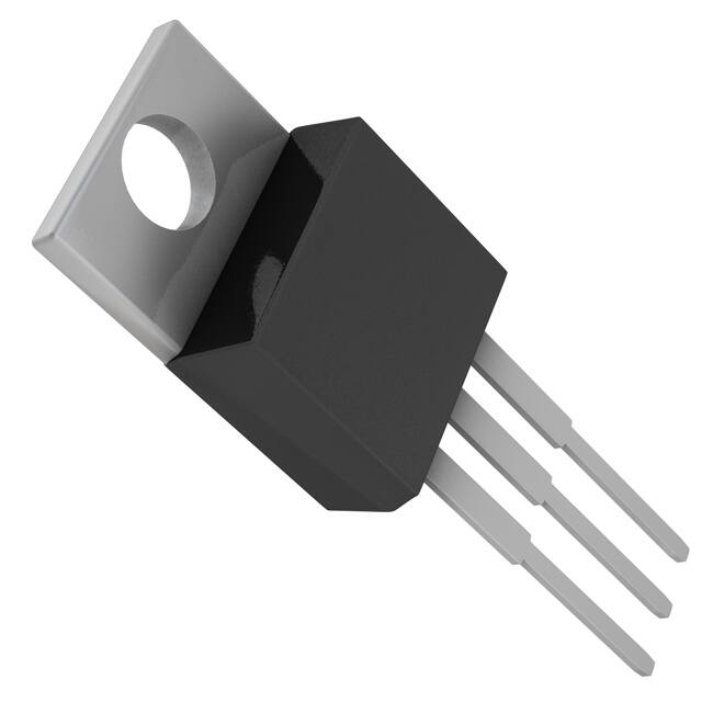
nn Available in 3-Lead Plastic TO-220 and DD Packages
The LT®1083 series of positive adjustable regulators are
designed to provide 7.5A, 5A and 3A with higher efficiency
than currently available devices. All internal circuitry is
designed to operate down to 1V input-to-output differential
and the dropout voltage is fully specified as a function of
load current. Dropout is guaranteed at a maximum of 1.5V
at maximum output current, decreasing at lower load currents. On-chip trimming adjusts the reference voltage to
1%. Current limit is also trimmed, minimizing the stress
on both the regulator and power source circuitry under
overload conditions.
nn
Applications
The LT1083/LT1084/LT1085 devices are pin compatible
with older 3-terminal regulators. A 10µF output capacitor
is required on these new devices. However, this is included
in most regulator designs.
High Efficiency Linear Regulators
nn Post Regulators for Switching Supplies
nn Constant Current Regulators
nn Battery Chargers
nn
DEVICE
OUTPUT CURRENT*
LT1083
LT1084
LT1085
7.5A
5.0A
3.0A
Unlike PNP regulators, where up to 10% of the output current is wasted as quiescent current, the LT1083 quiescent
current flows into the load, increasing efficiency.
L, LT, LTC, LTM, Linear Technology and the Linear logo are registered trademarks and
UltraFast and ThinSOT are trademarks of Linear Technology Corporation. All other trademarks
are the property of their respective owners.
*For a 1.5A low dropout regulator see the LT1086 data sheet.
Typical Application
5V, 7.5A Regulator
VIN ≥ 6.5V
IN
+
LT1083
ADJ
10µF
5V AT 7.5A
OUT
121Ω
1%
+
10µF*
TANTALUM
365Ω
1%
*REQUIRED FOR STABILITY
1083/4/5 ADJ TA01
INPUT/OUTPUT VOLTAGE DIFFERENTIAL (V)
Dropout Voltage vs Output Current
2
1
0
0
IFULL LOAD
OUTPUT CURRENT
1083/4/5 ADJ TA02
108345fh
For more information www.linear.com/LT1083
1
�LT1083/LT1084/LT1085
Absolute Maximum Ratings
(Note 1)
Power Dissipation................................ Internally Limited
Input-to-Output Voltage Differential
C-Grades................................................................30V
I-Grades.................................................................30V
M-Grades (OBSOLETE).........................................35V
Operating Junction Temperature Range (Note 9)
C-Grades: Control Section.................... 0°C to 125°C
Power Transistor.................. 0°C to 150°C
I-Grades: Control Section................– 40°C to 125°C
Power Transistor..............– 40°C to 150°C
M-Grades: (OBSOLETE)
Control Section................– 55°C to 150°C
Power Transistor.............. –55°C to 200°C
Storage Temperature Range...................– 65°C to 150°C
Lead Temperature (Soldering, 10 sec).................... 300°C
Preconditioning
100% thermal shutdown functional test.
Pin Configuration
TAB IS
OUTPUT
FRONT VIEW
TAB
IS
OUTPUT
3
VIN
3
VIN
2
VOUT
2
VOUT
ADJ
1
ADJ
1
P PACKAGE
3-LEAD PLASTIC TO-3P
θJA = 35°C/W
T PACKAGE
3-LEAD PLASTIC TO-220
θJA = 50°C/W
OBSOLETE PACKAGE
BOTTOM VIEW
FRONT VIEW
CASE IS
OUTPUT
VIN
2
TAB
IS
OUTPUT
1
K PACKAGE
2-LEAD TO-3 METAL CAN
θJA = 35°C/W
OBSOLETE PACKAGE
3
VIN
2
VOUT
1
ADJ
M PACKAGE
3-LEAD PLASTIC DD
ADJ
2
FRONT VIEW
θJA = 30°C/W*
*WITH PACKAGE SOLDERED TO 0.5IN2 COPPER AREA OVER
BACKSIDE GROUND PLANE OR INTERNAL POWER PLANE. θJA CAN VARY
FROM 20°C/W TO >40°C/W DEPENDING ON MOUNTING TECHNIQUE
108345fh
For more information www.linear.com/LT1083
�LT1083/LT1084/LT1085
Order Information
LEAD FREE FINISH
TAPE AND REEL
PART MARKING
PACKAGE DESCRIPTION
TEMPERATURE RANGE
LT1083CP#PBF
NA
LT1083CP
3-Lead Plastic TO-3P
Control: 0°C to 125°C
Power: 0°C to 150°C
LT1084CP#PBF
NA
LT1084CP
3-Lead Plastic TO-3P
Control: 0°C to 125°C
Power: 0°C to 150°C
LT1084CT#PBF
NA
LT1084CT
3-Lead Plastic TO-220
Control: 0°C to 125°C
Power: 0°C to 150°C
LT1084IT#PBF
NA
LT1084IT
3-Lead Plastic TO-220
Control: –40°C to 125°C
Power: –40°C to 150°C
LT1085CT#PBF
NA
LT1085CT
3-Lead Plastic TO-220
Control: 0°C to 125°C
Power: 0°C to 150°C
LT1085IT#PBF
NA
LT1085IT
3-Lead Plastic TO-220
Control: –40°C to 125°C
Power: –40°C to 150°C
LT1085CM#PBF
LT1085CM#TRPBF
LT1085CM
3-Lead Plastic DD
Control: 0°C to 125°C
Power: 0°C to 150°C
LT1085IM#PBF
LT1085IM#TRPBF
LT1085IM
3-Lead Plastic DD
Control: –40°C to 125°C
Power: –40°C to 150°C
OBSOLETE PACKAGE
LEAD BASED FINISH
TAPE AND REEL
PART MARKING
PACKAGE DESCRIPTION
TEMPERATURE RANGE
LT1083CP
NA
LT1083CP
3-Lead Plastic TO-3P
Control: 0°C to 125°C
Power: 0°C to 150°C
LT1084CP
NA
LT1084CP
3-Lead Plastic TO-3P
Control: 0°C to 125°C
Power: 0°C to 150°C
OBSOLETE PACKAGE
LT1084CT
NA
LT1084CT
3-Lead Plastic TO-220
Control: 0°C to 125°C
Power: 0°C to 150°C
LT1084IT
NA
LT1084IT
3-Lead Plastic TO-220
Control: –40°C to 125°C
Power: –40°C to 150°C
LT1085CT
NA
LT1085CT
3-Lead Plastic TO-220
Control: 0°C to 125°C
Power: 0°C to 150°C
LT1085IT
NA
LT1085IT
3-Lead Plastic TO-220
Control: –40°C to 125°C
Power: –40°C to 150°C
LT1085CM
LT1085CM#TR
LT1085CM
3-Lead Plastic DD
Control: 0°C to 125°C
Power: 0°C to 150°C
LT1085IM
LT1085IM#TR
LT1085IM
3-Lead Plastic DD
Control: –40°C to 125°C
Power: –40°C to 150°C
108345fh
For more information www.linear.com/LT1083
3
�LT1083/LT1084/LT1085
Order Information
LEAD BASED FINISH
TAPE AND REEL
PART MARKING
PACKAGE DESCRIPTION
TEMPERATURE RANGE
LT1083CK
NA
LT1083CK
2-Lead TO-3 Metal Can
Control: 0°C to 125°C
Power: 0°C to 150°C
LT1083MK
NA
LT1083MK
2-Lead TO-3 Metal Can
Control: –55°C to 150°C
Power: –55°C to 200°C
LT1084CK
NA
LT1084CK
2-Lead TO-3 Metal Can
Control: 0°C to 125°C
Power: 0°C to 150°C
LT1084MK
NA
LT1084MK
2-Lead TO-3 Metal Can
Control: –55°C to 150°C
Power: –55°C to 200°C
LT1085CK
NA
LT1085CK
2-Lead TO-3 Metal Can
Control: 0°C to 125°C
Power: 0°C to 150°C
LT1085MK
NA
LT1085MK
2-Lead TO-3 Metal Can
Control: –55°C to 150°C
Power: –55°C to 200°C
OBSOLETE PACKAGE
Consult LTC Marketing for parts specified with wider operating temperature ranges.
For more information on lead free part marking, go to: http://www.linear.com/leadfree/
For more information on tape and reel specifications, go to: http://www.linear.com/tapeandreel/
4
108345fh
For more information www.linear.com/LT1083
�LT1083/LT1084/LT1085
Electrical Characteristics
The l denotes the specifications which apply over the full operating
temperature range, otherwise specifications are at TA = 25°C.
PARAMETER
CONDITIONS
Reference Voltage
IOUT = 10mA, TJ = 25°C,
(VIN – VOUT) = 3V
10mA ≤ IOUT ≤ IFULL_LOAD
1.5V ≤ (VIN – VOUT) ≤ 25V (Notes 4, 6, 7)
Line Regulation
Load Regulation
Dropout Voltage
Current Limit
LT1083
LT1084
LT1085
MIN
TYP
MAX
UNITS
1.238
1.250
1.262
V
1.225
1.250
1.270
V
l
0.015
0.035
0.2
0.2
%
%
M-Grade: 15V ≤ (VIN – VOUT) ≤ 35V (Notes 2, 3)
l
0.05
0.5
%
C-, I-Grades: 15V ≤ (VIN – VOUT) ≤ 30V (Notes 2, 3)
l
0.05
0.5
%
(VIN – VOUT) = 3V, 10mA ≤ IOUT ≤ IFULL_LOAD, TJ = 25°C
(Notes 2, 3, 4, 6)
l
0.1
0.2
0.3
0.4
%
%
∆VREF = 1%, IOUT = IFULL_LOAD (Notes 5, 6, 8)
l
1.3
1.5
V
(VIN – VOUT) = 5V
(VIN – VOUT) = 25V
(VIN – VOUT) = 5V
(VIN – VOUT) = 25V
(VIN – VOUT) = 5V
(VIN – VOUT) = 25V
l
l
l
l
l
l
l
l
ILOAD = 10mA, 1.5V ≤ (VIN – VOUT) ≤ 15V, TJ = 25°C (Notes 2, 3)
Minimum Load Current
(VIN – VOUT) = 25V
Thermal Regulation
LT1083
LT1084
LT1085
TA = 25°C, 30ms Pulse
Ripple Rejection
f = 120Hz, CADJ = 25µF, COUT = 25µF Tantalum
IOUT = IFULL_LOAD, (VIN – VOUT) = 3V (Notes 6, 7, 8)
Adjust Pin Current
TJ = 25°C
l
8.0
0.4
5.5
0.3
3.2
0.2
60
5
10
mA
0.002
0.003
0.004
0.010
0.015
0.020
%/W
%/W
%/W
75
55
l
Adjust Pin Current Change
10mA ≤ IOUT ≤ IFULL_LOAD, 1.5V ≤ (VIN – VOUT) ≤ 25V (Note 6)
Temperature Stability
Long-Term Stability
TA = 125°C, 1000 Hrs
RMS Output Noise (% of VOUT)
TA = 25°C, 10Hz = ≤ f ≤ 10kHz
Thermal Resistance Junction-to-Case
LT1083
Control Circuitry/Power Transistor
K Package
P Package
K Package
P Package
T Package
K Package
M, T Package
LT1084
LT1085
A
A
A
A
A
A
9.5
1.0
6.5
0.6
4.0
0.5
l
0.2
l
0.5
0.3
dB
120
µA
µA
5
µA
%
1
0.003
%
%
0.6/1.6
0.5/1.6
0.75/2.3
0.65/2.3
0.65/2.7
0.9/3.0
0.7/3.0
°C/W
°C/W
°C/W
°C/W
°C/W
°C/W
°C/W
108345fh
For more information www.linear.com/LT1083
5
�LT1083/LT1084/LT1085
electrical characteristics
Note 1: Stresses beyond those listed under Absolute Maximum Ratings
may cause permanent damage to the device. Exposure to any Absolute
Maximum Rating condition for extended periods may affect device
reliability and lifetime.
Note 2: See thermal regulation specifications for changes in output voltage
due to heating effects. Load and line regulation are measured at a constant
junction temperature by low duty cycle pulse testing.
Note 3: Line and load regulation are guaranteed up to the maximum power
dissipation (60W for the LT1083, 45W for the LT1084 (K, P), 30W for the
LT1084 (T) and 30W for the LT1085). Power dissipation is determined by
the input/output differential and the output current. Guaranteed maximum
power dissipation will not be available over the full input/output voltage
range.
6
Note 4: IFULL_LOAD is defined in the current limit curves. The IFULL_LOAD
curve is defined as the minimum value of current limit as a function of
input-to-output voltage. Note that the 60W power dissipation for the
LT1083 (45W for the LT1084 (K, P), 30W for the LT1084 (T), 30W for the
LT1085) is only achievable over a limited range of input-to-output voltage.
Note 5: Dropout voltage is specified over the full output current range of
the device. Test points and limits are shown on the Dropout Voltage curve.
Note 6: For LT1083 IFULL_LOAD is 5A for – 55°C ≤ TJ < – 40°C and 7.5A for
TJ ≥ –40°C.
Note 7: 1.7V ≤ (VIN – VOUT) ≤ 25V for LT1084 at – 55°C ≤ TJ ≤ – 40°C.
Note 8: Dropout is 1.7V maximum for LT1084 at – 55°C ≤ TJ ≤ –40°C.
Note 9: The LT1083/LT1084/LT1085 regulators are tested and specified
under pulse load conditions such that TJ ≅ TA. The C-grade LT1083/
LT1084/LT1085 are 100% tested at 25°C.The I-grade LT1084/LT1085 are
guaranteed over the full –40°C to 125°C operating ambient temperature
range.
108345fh
For more information www.linear.com/LT1083
�LT1083/LT1084/LT1085
Typical Performance Characteristics
LT1083
Short-Circuit Current
12
INDICATES GUARANTEED TEST POINT
TJ = 150°C
TJ = 25°C
TJ = –55°C
1
2
3 4 5 6 7 8
OUTPUT CURRENT (A)
9
6
–55°C
4
2
0
10
150°C
8
IFULL LOAD
GUARANTEED
0
20
30
15
25
5
10
INPUT/OUTPUT DIFFERENTIAL (V)
LT1083/4/5 ADJ G01
SHORT-CIRCUIT CURRENT (A)
MINIMUN INPUT/OUTPUT DIFFERENTIAL (V)
TJ = –55°C
TJ = 25°C
1
3
4
2
OUTPUT CURRENT (A)
5
150°C
25°C
6
–55°C
5
4
3
2
0
6
IFULL LOAD
GUARANTEED
0
20
15
10
25
30
5
INPUT/OUTPUT DIFFERENTIAL (V)
–0.10
–0.15
TJ = –55°C
TJ = 25°C
3
2
1
OUTPUT CURRENT (A)
0
25 50 75 100 125 150
TEMPERATURE (°C)
LT1083/4/5 ADJ G06
LT1085
Load Regulation
0.10
∆I = 3A
SHORT-CIRCUIT CURRENT (A)
MINIMUM INPUT/OUTPUT DIFFERENTIAL (V)
–0.05
–0.20
–50 –25
35
6
–55°C ≤ TJ ≤ 150°C
0
0
LT1085
Short-Circuit Current
0°C ≤ TJ ≤ 125°C
0
0.05
LT1083/4/5 ADJ G05
INDICATES GUARANTEED TEST POINT
TJ = 150°C
LT1084
Load Regulation
8
7
LT1085
Dropout Voltage
1
25 50 75 100 125 150
TEMPERATURE (°C)
∆I = 5A
LT1083/4/5 ADJ G04
2
0
0.10
1
0
–0.15
9
0°C ≤ TJ ≤ 125°C
0
–0.10
LT1083/4/5 ADJ G03
10
–55°C ≤ TJ ≤ 150°C
TJ = 150°C
–0.05
LT1084
Short-Circuit Current
INDICATES GUARANTEED TEST POINT
1
0
LT1083/4/5 ADJ G02
LT1084
Dropout Voltage
2
0.05
–0.20
–50 –25
35
OUTPUT VOLTAGE DEVIATION (%)
0
25°C
10
OUTPUT VOLTAGE DEVIATION (%)
0°C ≤ TJ ≤ 125°C
0
0.10
∆I = 7.5A
–40°C ≤ TJ ≤ 150°C
1
LT1083
Load Regulation
4
LT1083/4/5 ADJ G07
OUTPUT VOLTAGE DEVIATION (%)
2
SHORT-CIRCUIT CURRENT (A)
MINIMUM INPUT/OUTPUT DIFFERENTIAL (V)
LT1083
Dropout Voltage
5
25°C
4
150°C
3
–55°C
2
IFULL LOAD
GUARANTEED
1
0
0
20
30
15
25
5
10
INPUT/OUTPUT DIFFERENTIAL (V)
35
LT1083/4/5 ADJ G08
0.05
0
–0.05
–0.10
–0.15
–0.20
–50 –25
0
25 50 75 100 125 150
TEMPERATURE (°C)
LT1083/4/5 ADJ G09
108345fh
For more information www.linear.com/LT1083
7
�LT1083/LT1084/LT1085
Typical Performance Characteristics
Minimum Operating Current
8
7
6
5
TJ = 150°C
4
TJ = 25°C
3
2
ADJUST PIN CURRENT (µA)
90
REFERENCE VOLTAGE (V)
1.26
1.25
1.24
TJ = –55°C
0
20
15
10
25
30
5
INPUT/OUTPUT DIFFERENTIAL (V)
35
0
60
40
30
CADJ = 200µF AT FREQUENCIES < 60Hz
CADJ = 25µF AT FREQUENCIES > 60Hz
IOUT = 7A
20
10
0
10
100
1k
10k
FREQUENCY (Hz)
100k
30
0
CADJ = 200µF AT FREQUENCIES < 60Hz
CADJ = 25µF AT FREQUENCIES > 60Hz
IOUT = 5A
10
100
1k
10k
FREQUENCY (Hz)
1083/4/5 ADJ G16
8
7
50 60 70 80 90 100 110 120 130 140 150
CASE TEMPERATURE (°C)
* AS LIMITED BY MAXIMUM JUNCTION TEMPERATURE
8
LT1083/4/5 ADJ G15
LT1084
Maximum Power Dissipation*
60
50
LT1084MK
fR = 20kHz
VRIPPLE ≤ 0.5VP-P
70
60
40
50
40
30
VOUT = 5V
CADJ = 25µF
COUT = 25µF
20
0
30
20
10
100k
LT1083CK
0
fR = 120Hz
VRIPPLE ≤ 3VP-P
90
RIPPLE REJECTION (dB)
30
LT1083CP
10
6
4
3
2
5
OUTPUT CURRENT (A)
1
80
40
10
40
LT1084
Ripple Rejection vs Current
(VIN – VOUT) ≥ VDROPOUT
20
50
20
100
50
LT1083MK
60
30
VOUT = 5V
CADJ = 25µF
COUT = 25µF
20
1083/4/5 ADJ G14
VRIPPLE ≤ 3VP-P VRIPPLE ≤ 0.5VP-P
60
0
70
40
0
100
70
25 50 75 100 125 150
TEMPERATURE (°C)
90
50
10
(VIN – VOUT) ≥ 3V
0
80
60
LT1084
Ripple Rejection
80
20
100
fR = 20kHz
VRIPPLE ≤ 0.5VP-P
70
1083/4/5 ADJ G13
90
30
LT1083
Maximum Power Dissipation*
80
(VIN – VOUT) ≥ VDROPOUT
50
40
LT1083/4/5 ADJ G12
fR = 120Hz
VRIPPLE ≤ 3VP-P
90
RIPPLE REJECTION (dB)
RIPPLE REJECTION (dB)
100
VRIPPLE
≤ 0.5VP-P
(VIN – VOUT) ≥ 3V
70
50
LT1083
Ripple Rejection vs Current
VRIPPLE ≤ 3VP-P
80
60
LT1083/4/5 ADJ G11
LT1083
Ripple Rejection
90
70
0
–50 –25
25 50 75 100 125 150
TEMPERATURE (°C)
LT1083/4/5 ADJ G10
100
80
10
1.23
–50 –25
POWER (W)
1
POWER (W)
MINIMUM OPERATING CURRENT (mA)
100
1.27
9
0
RIPPLE REJECTION (dB)
Adjust Pin Current
Temperature Stability
10
0
1
10
4
3
2
OUTPUT CURRENT (A)
5
1083/4/5 ADJ G17
LT1084CT
LT1084CP
LT1084CK
0
50 60 70 80 90 100 110 120 130 140 150
CASE TEMPERATURE (°C)
* AS LIMITED BY MAXIMUM JUNCTION TEMPERATURE
LT1083/4/5 ADJ G18
108345fh
For more information www.linear.com/LT1083
�LT1083/LT1084/LT1085
Typical Performance Characteristics
LT1085
Ripple Rejection
(VIN – VOUT) ≥ VDROPOUT
50
40
30
CADJ = 200µF AT FREQUENCIES < 60Hz
CADJ = 25µF AT FREQUENCIES > 60Hz
IOUT = 3A
20
10
10
100
1k
10k
FREQUENCY (Hz)
60
fR = 20kHz
VRIPPLE ≤ 0.5VP-P
50
40
VOUT = 5V
CADJ = 25µF
COUT = 25µF
20
10
0
100k
0
0.5
LT1085CK
2.0
1.0
1.5
OUTPUT CURRENT (A)
0.4
OUTPUT VOLTAGE
DEVIATION (V)
0.6
0.4
0
CIN = 1µF
COUT = 10µF TANTALUM
–0.4
LOAD CURRENT (A)
8
VOUT=10V
VIN=13V
PRELOAD=100mA
6
4
2
0
50
TIME (µs)
0
100
LOAD CURRENT (A)
OUTPUT VOLTAGE
DEVIATION (V)
0.6
–0.2
LT1083/4/5 ADJ G21
LT1085
Load Transient Response
0.3
CADJ = 1µF
0.2
0
–0.2
CIN = 1µF
COUT = 10µF TANTALUM
–0.4
–0.6
6
VOUT=10V
VIN=13V
PRELOAD=100mA
4
2
0
50
TIME (µs)
0
100
OUTPUT VOLTAGE
DEVIATION (mV)
CADJ = 1µF
50
0
–50
–100
VOUT = 10V
IIN = 0.2A
CIN = 1µF TANTALUM
COUT = 10µF TANTALUM
14
13
12
0
100
TIME (µs)
–0.1
200
1083/4/5 ADJ G25
CIN = 1µF
COUT = 10µF TANTALUM
–0.2
–0.3
3
VOUT=10V
VIN=13V
PRELOAD=100mA
2
1
0
50
TIME (µs)
0
100
LT1085
Line Transient Response
60
CADJ = 0
40
CADJ = 1µF
20
0
–20
–40
VOUT = 10V
IIN = 0.2A
CIN = 1µF TANTALUM
COUT = 10µF TANTALUM
–60
INPUT
DEVIATION (V)
–150
0
1083/4/5 ADJ G24
60
CADJ = 0
CADJ = 1µF
0.1
LT1084
Line Transient Response
150
100
CADJ = 0
0.2
1083/4/5 ADJ G23
LT1083
Line Transient Response
OUTPUT VOLTAGE
DEVIATION (mV)
50 60 70 80 90 100 110 120 130 140 150
CASE TEMPERATURE (°C)
* AS LIMITED BY MAXIMUM JUNCTION TEMPERATURE
3.0
CADJ = 0
1083/4/5 ADJ G22
INPUT
DEVIATION (V)
2.5
LT1084
Load Transient Response
CADJ = 1µF
LT1085CT
0
1083/4/5 ADJ G20
LT1083
Load Transient Response
0.2
20
10
1083/4/5 ADJ G19
CADJ = 0
LT1085MK
30
30
OUTPUT VOLTAGE
DEVIATION (mV)
0
40
fR = 120Hz
VRIPPLE ≤ 3VP-P
70
OUTPUT VOLTAGE
DEVIATION (V)
60
80
POWER (W)
(VIN – VOUT) ≥ 3V
70
50
90
14
13
12
0
100
TIME (µs)
CADJ = 0
40
CADJ = 1µF
20
0
–20
–40
VOUT = 10V
IIN = 0.2A
CIN = 1µF TANTALUM
COUT = 10µF TANTALUM
–60
INPUT
DEVIATION (V)
RIPPLE REJECTION (dB)
80
100
VRIPPLE
≤ 0.5VP-P
LOAD CURRENT (A)
VRIPPLE ≤ 3VP-P
90
RIPPLE REJECTION (dB)
100
LT1085
Maximum Power Dissipation*
LT1085
Ripple Rejection vs Current
200
1083/4/5 ADJ G26
14
13
12
0
100
TIME (µs)
200
1083/4/5 ADJ G27
108345fh
For more information www.linear.com/LT1083
9
�LT1083/LT1084/LT1085
Block Diagram
VIN
+
–
THERMAL
LIMIT
VOUT
1083/4/5 ADJ BD
VADJ
Applications Information
The LT1083 family of 3-terminal adjustable regulators is
easy to use and has all the protection features that are
expected in high performance voltage regulators. They are
short-circuit protected, and have safe area protection as
well as thermal shutdown to turn off the regulator should
the junction temperature exceed about 165°C.
These regulators are pin compatible with older 3-terminal
adjustable devices, offer lower dropout voltage and more
precise reference tolerance. Further, the reference stability
with temperature is improved over older types of regulators. The only circuit difference between using the LT1083
family and older regulators is that this new family requires
an output capacitor for stability.
Stability
The circuit design used in the LT1083 family requires the
use of an output capacitor as part of the device frequency
compensation. For all operating conditions, the addition of
a 150µF aluminium electrolytic or a 22µF solid tantalum
10
on the output will ensure stability. Normally, capacitors
much smaller than this can be used with the LT1083. Many
different types of capacitors with widely varying characteristics are available. These capacitors differ in capacitor
tolerance (sometimes ranging up to ±100%), equivalent
series resistance, and capacitance temperature coefficient.
The 150µF or 22µF values given will ensure stability.
When the adjustment terminal is bypassed to improve the
ripple rejection, the requirement for an output capacitor
increases. The value of 22µF tantalum or 150µF aluminum
covers all cases of bypassing the adjustment terminal.
Without bypassing the adjustment terminal, smaller
capacitors can be used with equally good results and the
table below shows approximately what size capacitors are
needed to ensure stability.
Recommended Capacitor Values
INPUT
OUTPUT
ADJUSTMENT
10µF
10µF
10µF Tantalum, 50µF Aluminum
22µF Tantalum, 150µF Aluminum
None
20µF
108345fh
For more information www.linear.com/LT1083
�LT1083/LT1084/LT1085
Applications Information
Normally, capacitor values on the order of 100µF are used
in the output of many regulators to ensure good transient
response with heavy load current changes. Output capacitance can be increased without limit and larger values of
output capacitor further improve stability and transient
response of the LT1083 regulators.
pin instantaneously shorted to ground, can damage occur.
A crowbar circuit at the input of the LT1083 can generate
those kinds of currents, and a diode from output to input is
then recommended. Normal power supply cycling or even
plugging and unplugging in the system will not generate
current large enough to do any damage.
Another possible stability problem that can occur in monolithic IC regulators is current limit oscillations. These can
occur because, in current limit, the safe area protection
exhibits a negative impedance. The safe area protection
decreases the current limit as the input-to-output voltage increases. That is the equivalent of having a negative
resistance since increasing voltage causes current to
decrease. Negative resistance during current limit is not
unique to the LT1083 series and has been present on all
power IC regulators. The value of the negative resistance
is a function of how fast the current limit is folded back
as input-to-output voltage increases. This negative resistance can react with capacitors or inductors on the input
to cause oscillation during current limiting. Depending
on the value of series resistance, the overall circuitry may
end up unstable. Since this is a system problem, it is not
necessarily easy to solve; however, it does not cause any
problems with the IC regulator and can usually be ignored.
The adjustment pin can be driven on a transient basis
± 25V, with respect to the output without any device degradation. Of course, as with any IC regulator, exceeding
the maximum input to output voltage differential causes
the internal transistors to break down and none of the
protection circuitry is functional.
Protection Diodes
In normal operation, the LT1083 family does not need
any protection diodes. Older adjustable regulators required protection diodes between the adjustment pin and
the output and from the output to the input to prevent
overstressing the die. The internal current paths on the
LT1083 adjustment pin are limited by internal resistors.
Therefore, even with capacitors on the adjustment pin, no
protection diode is needed to ensure device safety under
short-circuit conditions.
Diodes between input and output are usually not needed.
The internal diode between the input and the output pins
of the LT1083 family can handle microsecond surge currents of 50A to 100A. Even with large output capacitances,
it is very difficult to get those values of surge currents
in normal operations. Only with a high value of output
capacitors, such as 1000µF to 5000µF and with the input
D1
1N4002
(OPTIONAL)
VIN
IN
LT1083
OUT
ADJ
+
R1
CADJ
10µF
+
VOUT
COUT
150µF
R2
1083/4/5 ADJ F00
Overload Recovery
Like any of the IC power regulators, the LT1083 has safe
area protection. The safe area protection decreases the
current limit as input-to-output voltage increases and
keeps the power transistor inside a safe operating region
for all values of input-to-output voltage. The LT1083
protection is designed to provide some output current
at all values of input-to-output voltage up to the device
breakdown.
When power is first turned on, as the input voltage rises,
the output follows the input, allowing the regulator to start
up into very heavy loads. During the start-up, as the input
voltage is rising, the input-to-output voltage differential
remains small, allowing the regulator to supply large
output currents. With high input voltage, a problem can
occur wherein removal of an output short will not allow
the output voltage to recover. Older regulators, such as
the 7800 series, also exhibited this phenomenon, so it is
not unique to the LT1083.
108345fh
For more information www.linear.com/LT1083
11
�LT1083/LT1084/LT1085
Applications Information
The problem occurs with a heavy output load when the
input voltage is high and the output voltage is low, such
as immediately after removal of a short. The load line for
such a load may intersect the output current curve at two
points. If this happens, there are two stable output operating points for the regulator. With this double intersection,
the power supply may need to be cycled down to zero and
brought up again to make the output recover.
Ripple Rejection
The typical curves for ripple rejection reflect values for a
bypassed adjustment pin. This curve will be true for all
values of output voltage. For proper bypassing and ripple
rejection approaching the values shown, the impedance
of the adjust pin capacitor at the ripple frequency should
be less than the value of R1, (normally 100Ω to 120Ω).
The size of the required adjust pin capacitor is a function
of the input ripple frequency. At 120Hz the adjust pin
capacitor should be 25µF if R1 = 100Ω. At 10kHz only
0.22µF is needed.
For circuits without an adjust pin bypass capacitor, the
ripple rejection will be a function of output voltage. The
output ripple will increase directly as a ratio of the output
voltage to the reference voltage (VOUT/VREF). For example,
with the output voltage equal to 5V and no adjust pin capacitor, the output ripple will be higher by the ratio of 5V/1.25V
or four times larger. Ripple rejection will be degraded by
12dB from the value shown on the typical curve.
Output Voltage
12
OUT
LT1083
ADJ
VOUT
VREF
R1
IADJ
50µA
(
R2
)
VOUT = VREF 1 + R2 + IADJ R2
R1
1083/4/5 ADJ F01
Figure 1. Basic Adjustable Regulator
Load Regulation
Because the LT1083 is a 3-terminal device, it is not possible to provide true remote load sensing. Load regulation
will be limited by the resistance of the wire connecting
the regulator to the load. The data sheet specification for
load regulation is measured at the bottom of the package.
Negative side sensing is a true Kelvin connection, with the
bottom of the output divider returned to the negative side
of the load. Although it may not be immediately obvious,
best load regulation is obtained when the top of the resistor divider R1 is connected directly to the case not to the
load. This is illustrated in Figure 2. If R1 were connected
to the load, the effective resistance between the regulator
and the load would be:
⎛ R2+R1⎞
RP • ⎜
⎟,RP = Parasitic Line Resistance
⎝ R1 ⎠
VIN
The LT1083 develops a 1.25V reference voltage between
the output and the adjust terminal (see Figure 1). By
placing a resistor R1 between these two terminals, a
constant current is caused to flow through R1 and down
through R2 to set the overall output voltage. Normally this
current is the specified minimum load current of 10mA.
Because IADJ is very small and constant when compared
with the current through R1, it represents a small error
and can usually be ignored.
IN
VIN
IN
LT1083
OUT
RP
PARASITIC
LINE RESISTANCE
ADJ
R1*
RL
R2*
*CONNECT R1 TO CASE
CONNECT R2 TO LOAD
1083/4/5 ADJ F02
Figure 2. Connections for Best Load Regulation
108345fh
For more information www.linear.com/LT1083
�LT1083/LT1084/LT1085
Applications Information
Connected as shown, RP is not multiplied by the divider
ratio. RP is about 0.004Ω per foot using 16-gauge wire. This
translates to 4mV/ft at 1A load current, so it is important
to keep the positive lead between regulator and load as
short as possible and use large wire or PC board traces.
Thermal Considerations
The LT1083 series of regulators have internal power and
thermal limiting circuitry designed to protect the device
under overload conditions. For continuous normal load
conditions however, maximum junction temperature ratings must not be exceeded. It is important to give careful
consideration to all sources of thermal resistance from
junction to ambient. This includes junction-to-case, caseto-heat sink interface, and heat sink resistance itself. New
thermal resistance specifications have been developed to
more accurately reflect device temperature and ensure
safe operating temperatures. The data section for these
new regulators provides a separate thermal resistance and
maximum junction temperature for both the Control Section
and the Power Transistor. Previous regulators, with a single
junction-to-case thermal resistance specification, used
an average of the two values provided here and therefore
could allow excessive junction temperatures under certain
conditions of ambient temperature and heat sink resistance.
To avoid this possibility, calculations should be made for
both sections to ensure that both thermal limits are met.
Junction-to-case thermal resistance is specified from the
IC junction to the bottom of the case directly below the
die. This is the lowest resistance path for heat flow. Proper
mounting is required to ensure the best possible thermal
flow from this area of the package to the heat sink. Thermal
compound at the case-to-heat sink interface is strongly
recommended. If the case of the device must be electrically isolated, a thermally conductive spacer can be used,
as long as its added contribution to thermal resistance is
considered. Note that the case of all devices in this series
is electrically connected to the output.
For example, using an LT1083CK (TO-3, Commercial)
and assuming:
VIN (Max Continuous) = 9V, VOUT = 5V, IOUT = 6A,
TA = 75°C, θHEAT SINK = 1°C/W,
θCASE-TO-HEAT SINK = 0.2°C/W for K package with
thermal compound.
Power dissipation under these conditions is equal to:
PD = (VIN – VOUT )(IOUT) = 24W
Junction temperature will be equal to:
TJ = TA + PD (θHEAT SINK + θCASE-TO-HEAT SINK + θJC)
For the Control Section:
TJ = 75°C + 24W (1°C/W + 0.2°C/W + 0.6°C/W) = 118°C
118°C < 125°C = TJMAX (Control Section
Commercial Range)
For the Power Transistor:
TJ = 75°C + 24W (1°C/W + 0.2°C/W + 1.6°C/W) = 142°C
142°C < 150°C = TJMAX (Power Transistor
Commercial Range)
In both cases the junction temperature is below the maximum rating for the respective sections, ensuring reliable
operation.
108345fh
For more information www.linear.com/LT1083
13
�LT1083/LT1084/LT1085
Typical Application
7.5A Variable Regulator
T1
TRIAD
F-269U
L
1mH
C30B
20Ω
3
110VAC
20Ω
IN
T2
1
C1
50,000µF
750Ω*
16k*
560Ω
15V
15k
–15V
8
2
3
10k
+
4
LT1011
–
200k
7
2.7k
–15V
NC
15V
7
16k*
11k*
0.1µF
–
4
3
1
LT1011
+
1
10k
2
15K
GENERAL PURPOSE REGULATOR WITH SCR PREREGULATOR
TO LOWER POWER DISSIPATION. ABOUT 1.7V DIFFERENTIAL
IS MAINTAINED ACROSS THE LT1083 INDEPENDENT OF OUTPUT
VOLTAGE AND LOAD CURRENT
100pF
2N3904
8
–15V
14
LT1004-1.2
1
1N4148
* 1% FILM RESISTOR
L: DALE TO-5 TYPE
T2: STANCOR 11Z-2003
100µF
2k
OUTPUT
ADJUST
1N4003
82k
0V TO 35V
OA TO 7.5A
2
1N914
1µF
1.5k
+
LT1004-1.2
C30B
1N4003
OUT
ADJ
+
1N4003
LT1083
8
6
+
3
–
2
LM301A
7
4
–15V
15V
15V
1µF
11k*
LT1083/4/5 ADJ TA05
108345fh
For more information www.linear.com/LT1083
�LT1083/LT1084/LT1085
Typical Application
Paralleling Regulators
VIN
IN
LT1083
2 FEET #18 WIRE*
OUT
( )
ADJ
VOUT = 1.25V 1 + R2
R1
IOUT = 0A TO 15A
0.015Ω
IN
LT1083
OUT
*THE #18 WIRE ACTS
AS BALLAST RESISTANCE
INSURING CURRENT SHARING
BETWEEN BOTH DEVICES
ADJ
R1
120Ω
LT1083/4/5 ADJ TA03
R2
Improving Ripple Rejection
VIN
IN
+
LT1083
OUT
VOUT
5V
R1
121Ω
1%
ADJ
10µF
R2
365Ω
1%
+
+
150µF
C1
25µF*
*C1 IMPROVES RIPPLE REJECTION.
XC SHOULD BE < R1 AT RIPPLE FREQUENCY
1083/4/5 ADJ TA04
Remote Sensing
VIN
IN
LT1083
RP
(MAX DROP 300mV)
OUT
+
ADJ
25Ω
+
10µF
121Ω
VIN
100µF
7
6
–
LM301A
1
8
+
4
365Ω
VOUT
5V
100pF
2
3
1k
RL
5µF
+
25Ω
RETURN
RETURN
1083/4/5 ADJ TA07
108345fh
For more information www.linear.com/LT1083
15
�LT1083/LT1084/LT1085
Typical Application
High Efficiency Regulator with Switching Preregulator
1mH
VIN
28V
MR1122
IN
+
LT1083
ADJ
10,000µF
240Ω
470Ω
10k
1N914
28V
1k
1M
VOUT
OUT
2k
4N28
10k
+
1083/4/5 ADJ TA06
LT1011
10k
–
28V
1N914
1.2V to 15V Adjustable Regulator
VIN
IN
+
LT1083
R1
90.9Ω
ADJ
C1*
10µF
VOUT†
OUT
+
C2
100µF
R2
1k
*NEEDED IF DEVICE IS FAR FROM FILTER CAPACITORS
(
†V
R2
OUT = 1.25V 1 +
R1
)
1083/4/5 ADJ TA08
5V Regulator with Shutdown*
VIN
IN
+
TTL
LT1083
ADJ
10µF
1k
VOUT
5V
OUT
2N3904
121Ω
1%
+
365Ω
1%
100µF
1k
*OUTPUT SHUTS DOWN TO 1.3V
16
1083/4/5 ADJ TA09
108345fh
For more information www.linear.com/LT1083
�LT1083/LT1084/LT1085
Package Description
Please refer to http://www.linear.com/designtools/packaging/ for the most recent package drawings.
K Package
2-Lead TO-3 Metal Can
(Reference LTC DWG # 05-08-1310)
.320 – .350
(8.13 – 8.89)
1.177 – 1.197
(29.90 – 30.40)
.760 – .775
(19.30 – 19.69)
.655 – .675
(16.64 – 17.15)
.060 – .135
(1.524 – 3.429)
.420 – .480
(10.67 – 12.19)
.038 – .043
(0.965 – 1.09)
.210 – .220
(5.33 – 5.59)
.425 – .435
(10.80 – 11.05)
.151 – .161
(3.86 – 4.09)
DIA, 2PLCS
.167 – .177
(4.24 – 4.49)
R
.067 – .077
(1.70 – 1.96)
.490 – .510
(12.45 – 12.95)
R
K2 (TO-3) 0801
OBSOLETE PACKAGE
108345fh
For more information www.linear.com/LT1083
17
�LT1083/LT1084/LT1085
Package Description
Please refer to http://www.linear.com/designtools/packaging/ for the most recent package drawings.
M Package
M Package
3-Lead
Plastic
DD DD
PakPak
3-Lead
Plastic
(Reference
LTC LTC
DWGDWG
# 05-08-1460
RevRev
F) F)
(Reference
# 05-08-1460
.256
(6.502)
.060
(1.524)
TYP
.060
(1.524)
.390 – .415
(9.906 – 10.541)
.165 – .180
(4.191 – 4.572)
.045 – .055
(1.143 – 1.397)
15°
.060
(1.524)
.183
(4.648)
.330 – .370
(8.382 – 9.398)
+.008
.004 –.004
+0.203
0.102 –0.102
(
.059
(1.499)
)
.095 – .115
(2.413 – 2.921)
.075
(1.905)
.300
(7.620)
+.012
.143 –.020
+0.305
3.632 –0.508
(
BOTTOM VIEW OF DD PAK
HATCHED AREA IS SOLDER PLATED
COPPER HEAT SINK
)
DETAIL A
.050
(1.270)
.100
(2.54)
BSC
.013 – .023
(0.330 – 0.584)
.050 ±.012
(1.270 ±0.305)
DETAIL A
0° – 7° TYP
.080
.420
.350
0° – 7° TYP
.420
.276
.325
.205
.585
.585
.320
.090
.100
.100
.070
RECOMMENDED SOLDER PAD LAYOUT
NOTE:
1. DIMENSIONS IN INCH/(MILLIMETER)
2. DRAWING NOT TO SCALE
18
.090
.070
M (DD3) 0212 REV F
RECOMMENDED SOLDER PAD LAYOUT
FOR THICKER SOLDER PASTE APPLICATIONS
108345fh
For more information www.linear.com/LT1083
�LT1083/LT1084/LT1085
Package Description
Please refer to http://www.linear.com/designtools/packaging/ for the most recent package drawings.
P Package
P Package
3-Lead Plastic TO-3P
(Similar to TO-247)
3-Lead
Plastic
to Rev
TO-247))
(Reference
LTC TO-3P
DWG # (Similar
05-08-1450
A)
(Reference LTC DWG # 05-08-1450 Rev A)
.515 – .580
(13.08 – 14.73)
.305 – .370
(7.75 – 9.40)
.560 – .620
(14.22 – 15.75)
.187 – .207
(4.75 – 5.26)
.620 – .640
(15.75 – 16.26)
.265 – .293
(6.73 – 7.44)
MOUNTING HOLE
18° – 22°
.115 – .145
(2.92 – 3.68)
DIA
.819 – .870
(20.80 – 22.10)
.635 – .720
(16.13 – 18.29)
.060 – .081
(1.52 – 2.06)
.170 – .215
(4.32 – 5.46)
EJECTOR PIN MARKS
.105 – .125
(2.67 – 3.18)
DIA
.580 – .600
(14.73 – 15.24)
3° – 7°
.104 – .145
(2.64 – 3.68)
.170
(4.32)
MAX
.780 – .800
(19.81 – 20.32)
BOTTOM VIEW OF TO-3P
HATCHED AREA IS SOLDER PLATED
COPPER HEAT SINK
NOTE:
1. DIMENSIONS IN INCH/(MILLIMETER)
2. DRAWING NOT TO SCALE
3. DIMENSIONS ARE INCLUSIVE OF PLATING
4. DIMENSIONS ARE EXCLUSIVE OF MOLD FLASH AND METAL BURR
5. MOLD FLASH SHALL NOT EXCEED .030" (.762mm)
.042 – .052
(1.07 – 1.32)
.074 – .084
(1.88 – 2.13)
.215
(5.46)
BSC
.113 – .123
(2.87 – 3.12)
.087 – .102
(2.21 – 2.59)
.020 – .040
(0.51 – 1.02)
P3 0512 REV A
OBSOLETE PACKAGE
108345fh
For more information www.linear.com/LT1083
19
�LT1083/LT1084/LT1085
Package Description
Please refer to http://www.linear.com/designtools/packaging/ for the most recent package drawings.
T Package
3-Lead
Plastic TO-220
T Package
(Reference
DWG #TO-220
05-08-1420)
3-LeadLTC
Plastic
(Reference LTC DWG # 05-08-1420)
.147 – .155
(3.734 – 3.937)
DIA
.390 – .415
(9.906 – 10.541)
.165 – .180
(4.191 – 4.572)
.045 – .055
(1.143 – 1.397)
.230 – .270
(5.842 – 6.858)
.460 – .500
(11.684 – 12.700)
.570 – .620
(14.478 – 15.748)
.330 – .370
(8.382 – 9.398)
.980 – 1.070
(24.892 – 27.178)
.520 – .570
(13.208 – 14.478)
.100
(2.540)
BSC
20
.028 – .038
(0.711 – 0.965)
.218 – .252
(5.537 – 6.401)
.050
(1.270)
TYP
.013 – .023
(0.330 – 0.584)
.095 – .115
(2.413 – 2.921)
T3 (TO-220) 0801
108345fh
For more information www.linear.com/LT1083
�LT1083/LT1084/LT1085
Revision History
(Revision history begins at Rev H)
REV
DATE
DESCRIPTION
H
06/15
Obsolete TO-3P package.
PAGE NUMBER
2, 19
108345fh
Information furnished by Linear Technology Corporation is believed to be accurate and reliable.
However, no responsibility is assumed for its use. Linear Technology Corporation makes no representation that the interconnection
of its circuits
as described
herein will not infringe on existing patent rights.
For more
information
www.linear.com/LT1083
21
�LT1083/LT1084/LT1085
Typical Applications
Automatic Light Control
Protected High Current Lamp Driver
12V
5A
VIN
IN
LT1083
OUT
ADJ
+
OUT
1.2k
100µF
10µF
LT1083
15V
IN
ADJ
TTL OR
CMOS
1083/4/5 ADJ TA11
10k
1083/4/5 ADJ TA10
Related Parts
PART NUMBER DESCRIPTION
COMMENTS
LT1129
700mA Micropower Low Dropout Regulator
50µA Quiescent Current
LT1175
500mA Negative Low Dropout Micropower Regulator
45µA IQ, 0.26V Dropout Voltage, SOT-223 Package
LT1185
3A Negative Low Dropout Regulator
VIN: –4.5V to –35V, 0.8V Dropout Voltage, DD-Pak and TO-220 Packages
LT1529
3A Low Dropout Regulator with 50µA IQ
500mV Dropout Voltage
LT1580
7A, Very Low Dropout Regulator
0.54V Dropout at 7A, Fixed 2.5VOUT and Adjustable
LT1581
10A, Very Low Dropout Regulator
0.63V Dropout at 10A, Fixed 2.5VOUT and Adjustable
LT1584/
LT1585/
LT1587
7A/4.6A/3A Fast Response LDOs
Fast Transient Response for Microprocessor Applications
LT1761 Series
100mA, Low Noise, Low Dropout Micropower Regulators
in SOT-23
20µA Quiescent Current, 20µVRMS Noise, SOT-23 Package
LT1762 Series
150mA, Low Noise, LDO Micropower Regulators
25µA Quiescent Current, 20µVRMS Noise, MSOP Package
LT1763 Series
500mA, Low Noise LDO Micropower Regulators
30µA Quiescent Current, 20µVRMS Noise, SO-8 Package
LT1764
3A Low Noise Fast Transient Response LDO
40µVRMS Noise, 5-Lead DD Package
LT1962
300mA, Low Noise LDO Micropower Regulator
20µVRMS Noise, MSOP Package
LT1963
1.5A, Low Noise, Fast Transient Response LDO
40µVRMS Noise, SOT-223 Package
LT1964
200mA, Low Noise, Negative LDO
340mV Dropout Voltage, Low Noise 30µVRMS, VIN = –1.8V to –20V,
ThinSOT™ and 3mm × 3mm DFN-8 Packages
LT3015
1.5A, Low Noise, Negative Linear Regulator with Precision
Current Limit
VIN: –1.8V to –30V, VOUT: –1.22V to –29.5V, Dropout Voltage: 310mV,
Precision Current Limit with Foldback, Low Output Noise: 60μVRMS (10Hz
to 100kHz), TO-220, DD-Pak, DFN and MSOP Packages
LT3080/
LT3080-1
1.1A, Parallelable, Low Noise, Low Dropout Linear Regulator 300mV Dropout Voltage (2-Supply Operation), Low Noise: 40µVRMS,
VIN: 1.2V to 36V, VOUT: 0V to 35.7V, Stable with Ceramic Caps, TO-220,
DD-Pak, SOT-223, MS8E and 3mm × 3mm DFN-8 Packages; "-1" Version
Has Integrated Internal Ballast Resistor
LT3090
600mA Low Noise Negative LDO with Programmable ILIMIT
22 Linear Technology Corporation
300mV Dropout Voltage, 18µVRMS Output Voltage Noise, Parallelable
50μA SET Pin Current: ±1% Initial Accuracy, Positive/Negative Current
Monitors Wide Input Voltage Range: –1.5V to –36V, Rail-to-Rail Output
Voltage Range: 0V to –32V
1630 McCarthy Blvd., Milpitas, CA 95035-7417
For more information www.linear.com/LT1083
(408) 432-1900 ● FAX: (408) 434-0507
●
www.linear.com/LT1083
108345fh
LT 0615 REV H • PRINTED IN USA
LINEAR TECHNOLOGY CORPORATION 1994
�


 工商网监
湘ICP备2023018690号
工商网监
湘ICP备2023018690号

