LT1208/LT1209
Dual and Quad
45MHz, 400V/µs Op Amps
U
DESCRIPTIO
FEATURES
■
■
■
■
■
■
■
■
■
■
45MHz Gain-Bandwidth
400V/µs Slew Rate
Unity-Gain Stable
7V/mV DC Gain, RL = 500Ω
3mV Maximum Input Offset Voltage
±12V Minimum Output Swing into 500Ω
Wide Supply Range: ±2.5V to ±15V
7mA Supply Current per Amplifier
90ns Settling Time to 0.1%, 10V Step
Drives All Capacitive Loads
The LT1208/LT1209 are dual and quad very high speed
operational amplifiers with excellent DC performance. The
LT1208/LT1209 feature reduced input offset voltage and
higher DC gain than devices with comparable bandwidth
and slew rate. Each amplifier is a single gain stage with
outstanding settling characteristics. The fast settling time
makes the circuit an ideal choice for data acquisition
systems. Each output is capable of driving a 500Ω load to
±12V with ±15V supplies and a 150Ω load to ±3V on ±5V
supplies. The amplifiers are also capable of driving large
capacitive loads which make them useful in buffer or cable
driver applications.
UO
APPLICATI
■
■
■
■
■
■
S
The LT1208/LT1209 are members of a family of fast, high
performance amplifiers that employ Linear Technology
Corporation’s advanced bipolar complementary
processing.
Wideband Amplifiers
Buffers
Active Filters
Video and RF Amplification
Cable Drivers
Data Acquisition Systems
UO
TYPICAL APPLICATI
1MHz, 4th Order Butterworth Filter
Inverter Pulse Response
909Ω
1.1k
909Ω
2.67k
VIN
220pF
–
47pF
1/2
LT1208
+
1.1k
2.21k
470pF
–
22pF
1/2
LT1208
+
VOUT
1208/09 TA01
1208/09 TA02
1
�LT1208/LT1209
W W
W
AXI U
U
ABSOLUTE
RATI GS
Total Supply Voltage (V + to V –) .............................. 36V
Differential Input Voltage ........................................ ±6V
Input Voltage ........................................................... ±VS
Output Short-Circuit Duration (Note 1) ........... Indefinite
Operating Temperature Range
LT1208C/LT1209C .......................... – 40°C to 85°C
Maximum Junction Temperature
Plastic Package ............................................. 150°C
Storage Temperature Range ................ – 65°C to 150°C
Lead Temperature (Soldering, 10 sec)................. 300°C
W
U
U
PACKAGE/ORDER I FOR ATIO
TOP VIEW
OUT A 1
8
V+
–IN A 2
7
OUT B
A
+IN A 3
V
–
B
4
–IN B
6
ORDER PART
NUMBER
OUT A 1
–IN A 2
LT1208CN8
TOP VIEW
–IN A 2
+IN A 3
14 OUT D
A
D
+IN B 5
–IN B 6
OUT B 7
11
B
C
CONTACT FACTORY FOR
MILITARY/883B PARTS
ORDER PART
NUMBER
8
OUT A 1
–IN A 2
V–
+IN A 3
LT1209CN
D
A
+IN B 5
–IN B 6
–IN C
OUT C
CONDITIONS
VOS
Input Offset Voltage
VS = ±5V (Note 2)
0°C to 70°C
VS = ±15V (Note 2)
0°C to 70°C
2
LT1209CS
B
C
12 +IN C
11 –IN C
10 OUT C
9
NC
VS = ±15V, TA = 25°C, RL = 1k, VCM = 0V, unless otherwise noted.
PARAMETER
Input Noise Voltage
Input Noise Current
15 –IN D
TJMAX = 150°C, θJA = 100°C/W
SYMBOL
Input Bias Current
ORDER PART
NUMBER
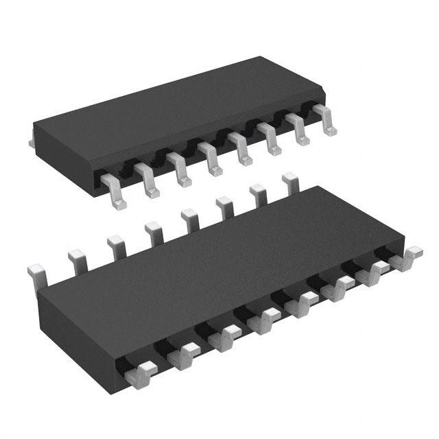
S PACKAGE
16-LEAD PLASTIC SOIC
ELECTRICAL CHARACTERISTICS
Input VOS Drift
Input Offset Current
1208
13 V –
OUT B 7
TJMAX = 150°C, θJA = 70°C/W
en
in
S8 PART MARKING
14 +IN D
V+ 4
N PACKAGE
14-LEAD PLASTIC DIP
IB
+IN B
16 OUT D
NC 8
IOS
5
LT1208CS8
TOP VIEW
10 +IN C
9
–IN B
TJMAX = 150°C, θJA = 150°C/W
13 –IN D
12 +IN D
V+ 4
OUT B
6
S8 PACKAGE
8-LEAD PLASTIC SOIC
TJMAX = 150°C, θJA = 100°C/W
OUT A 1
7
B
V– 4
N8 PACKAGE
8-LEAD PLASTIC DIP
8
V+
A
+IN A 3
+IN B
5
ORDER PART
NUMBER
TOP VIEW
VS = ±5V and VS = ±15V
0°C to 70°C
VS = ±5V and VS = ±15V
0°C to 70°C
f = 10kHz
f = 10kHz
MIN
TYP
MAX
UNITS
0.5
3.0
4.0
5.0
6.0
mV
mV
mV
mV
µV/°C
nA
nA
µA
µA
nV/√Hz
pA/√Hz
●
1.0
●
25
100
●
4
●
22
1.1
400
600
8
9
�LT1208/LT1209
ELECTRICAL CHARACTERISTICS
VS = ±15V, TA = 25°C, RL = 1k, VCM = 0V, unless otherwise noted.
SYMBOL
PARAMETER
CONDITIONS
MIN
TYP
RIN
Input Resistance
VCM = ±12V
Differential
20
CIN
CMRR
Input Capacitance
Common-Mode Rejection Ratio
40
250
2
98
PSRR
Power Supply Rejection Ratio
Input Voltage Range
AVOL
Large-Signal Voltage Gain
VOUT
Output Swing
IOUT
Output Current
SR
Slew Rate
GBW
Full Power Bandwidth
Gain-Bandwidth
tr, tf
Rise Time, Fall Time
Overshoot
Propagation Delay
ts
Settling Time
Differential Gain
Differential Phase
RO
IS
Output Resistance
Crosstalk
Supply Current
VS = ±15V, VCM = ±12V; VS = ±5V,
VCM = ±2.5V, 0°C to 70°C
VS = ±5V to ±15V
0°C to 70°C
VS = ±15V
VS = ±5V
VS = ±15V, VOUT = ±10V, RL = 500Ω
0°C to 70°C
VS = ± 5V, VOUT = ±2.5V, RL = 500Ω
0°C to 70°C
VS = ± 5V, VOUT = ±2.5V, RL = 150Ω
VS = ±15V, RL = 500Ω, 0°C to 70°C
VS = ±5V, RL = 150Ω, 0°C to 70°C
VS = ±15V, VOUT = ±12V, 0°C to 70°C
VS = ± 5V, VOUT = ± 3V, 0°C to 70°C
VS = ±15V, AVCL = – 2, (Note 3)
0°C to 70°C
VS = ±5V, AVCL = – 2, (Note 3)
0°C to 70°C
10V Peak, (Note 4)
VS = ±15V, f = 1MHz
VS = ±5V, f = 1MHz
VS = ±15V, AVCL = 1, 10% to 90%, 0.1V
VS = ± 5V, AVCL = 1, 10% to 90%, 0.1V
VS = ± 15V, AVCL = 1, 0.1V
VS = ± 5V, AVCL = 1, 0.1V
VS = ± 15V, 50% VIN to 50%VOUT
VS = ± 5V, 50% VIN to 50%VOUT
VS = ± 15V, 10V Step, VS = ±5V,
5V Step, 0.1%
f = 3.58MHz, RL = 150Ω
f = 3.58MHz, RL = 1k
f = 3.58MHz, RL = 150Ω
f = 3.58MHz, RL = 1k
AVCL = 1, f = 1MHz
VOUT = ±10V, RL = 500Ω
Each Amplifier, VS = ±5V and VS = ±15V
0°C to 70°C
The ● denotes the specifications which apply over the full operating
temperature range.
Note 1: A heat sink may be required to keep the junction temperature
below absolute maximum when the output is shorted indefinitely.
Note 2: Input offset voltage is tested with automated test equipment and is
exclusive of warm-up drift.
●
●
●
●
●
●
●
●
●
●
86
83
76
75
±12
±2.5
3.3
2.5
2.5
2.0
12.0
3.0
24
20
250
200
150
130
MAX
MΩ
kΩ
pF
dB
dB
dB
dB
V
V
V/mV
V/mV
V/mV
V/mV
V/mV
±V
±V
mA
mA
V/µs
V/µs
V/µs
V/µs
MHz
MHz
MHz
ns
ns
%
%
ns
ns
ns
84
±13
±3
7
7
3
13.3
3.3
40
40
400
250
6.4
45
34
5
7
30
20
5
7
90
1.30
0.09
1.8
0.1
2.5
–100
7
●
UNITS
– 94
9
10.5
%
%
Deg
Deg
Ω
dB
mA
mA
Note 3: Slew rate is measured in a gain of –2. For ±15V supplies measure
between ±10V on the output with ±6V on the input. For ±5V supplies
measure between ±2V on the output with ±1.75V on the input.
Note 4: Full power bandwidth is calculated from the slew rate
measurement: FPBW = SR/2πVP.
3
�LT1208/LT1209
U W
TYPICAL PERFOR A CE CHARACTERISTICS
Input Common-Mode Range vs
Supply Voltage
Supply Current vs Supply Voltage
and Temperature
20
10
SUPPLY CURRENT (mA)
15
10
+VCM
125°C
–VCM
5
8
OUTPUT VOLTAGE SWING (V)
MAGNITUDE OF INPUT VOLTAGE (V)
20
12
TA = 25°C
∆VOS < 1mV
25°C
6
–55°C
4
2
0
0
0
5
10
15
SUPPLY VOLTAGE (±V)
20
15
10
VS = ±5V
100
1k
LOAD RESISTANCE (Ω)
10k
4.5
TA = 25°C
90
2
4.0
3.5
4.00
3.75
3.50
–50 –25
25
75
0
50
TEMPERATURE (°C)
100
125
1208/09 G07
15
10
100
1k
LOAD RESISTANCE (Ω)
Input Noise Spectral Density
10000
100
VS = ±15V
TA = 25°C
AV = 101
RS = 100k
VS = ±5V
50
45
40
SOURCE
SINK
35
30
25
–50
10k
1208/09 G06
INPUT VOLTAGE NOISE (nV/√Hz)
OUTPUT SHORT-CIRCUIT CURRENT (mA)
4.25
VS = ±5V
–25
25
75
0
50
TEMPERATURE (°C)
100
125
1208/09 G08
in
1000
10
en
100
1
10
10
100
1k
10k
FREQUENCY (Hz)
0.1
100k
1208/09 G09
INPUT CURRENT NOISE (pA/√Hz)
4.50
70
50
–10
–5
0
5
10
INPUT COMMON-MODE VOLTAGE (V)
55
2
VS = ±15V
80
60
Output Short-Circuit Current
vs Temperature
5.00
4
Open-Loop Gain vs
Resistive Load
1208/09 G05
Input Bias Current vs Temperature
20
100
1208/09 G04
VS = ±15V
IB+ + IB–
IB =
5
10
15
SUPPLY VOLTAGE (±V)
1208/09 G03
VS = ±15V
TA = 25°C
I + + IB –
IB = B
3.0
–15
0
4.75
5
0
OPEN-LOOP GAIN (dB)
INPUT BIAS CURRENT (µA)
OUTPUT VOLTAGE SWING (VP-P)
VS = ±15V
10
–VSW
20
5.0
TA = 25°C
∆VOS = 30mV
5
+VSW
10
Input Bias Current vs Input
Common-Mode Voltage
30
20
15
1208/09 G02
Output Voltage Swing vs
Resistive Load
25
TA = 25°C
RL = 500Ω
∆VOS = 30mV
0
5
10
15
SUPPLY VOLTAGE (±V)
0
1208/09 G01
INPUT BIAS CURRENT (µA)
Output Voltage Swing vs
Supply Voltage
�LT1208/LT1209
U W
TYPICAL PERFOR A CE CHARACTERISTICS
Power Supply Rejection Ratio
vs Frequency
Crosstalk vs Frequency
100
CROSSTALK (dB)
–50
–60
–70
VS = ±5V
RL = 500Ω
–80
–90
VS = ±15V
RL = 1k
–100
–110
–120
100k
1M
10M
FREQUENCY (Hz)
120
VS = ±15V
TA = 25°C
80
+PSRR
60
–PSRR
40
20
0
100
100M
1k
10k 100k
1M
FREQUENCY (Hz)
Voltage Gain and Phase vs
Frequency
100
VS = ±5V
40
VS = ±5V
40
VS = ±15V
1k
6
AV = 1
AV = 1
–4
–6
0
100M
AV = –1
AV = –1
VS = ±15V
TA = 25°C
10mV SETTLING
4
C = 100pF
2
C = 50pF
0
–2
C=0
–4
C = 500pF
–6
C = 1000pF
–8
25
0
75
100
50
SETTLING TIME (ns)
1M
125
Slew Rate vs Temperature
500
VS = ±15V
450
0.1
46
45
44
100M
1208/09 G16
42
–50
400
+SR
350
300
250
43
1M
10M
FREQUENCY (Hz)
VS = ±15V
AV = –2
–SR
SLEW RATE (V/µs)
GAIN-BANDWIDTH (MHz)
47
1
100M
1208/09 G15
Gain-Bandwidth vs Temperature
VS = ±15V
TA = 25°C
AV = +1
10M
FREQUENCY (Hz)
1208/09 G14
48
100k
VS = ±15V
TA = 25°C
AV = –1
–10
–10
100
100M
10M
Frequency Response vs
Capacitive Load
6
–8
10M
100k
1M
FREQUENCY (Hz)
10k
1208/09 G12
8
–2
Closed-Loop Output Impedance
vs Frequency
0.01
10k
20
8
1208/09 B13
10
40
0
100M
0
TA = 25°C
1M
10k 100k
FREQUENCY (Hz)
60
10
2
20
0
1k
80
10
4
OUTPUT SWING (V)
60
PHASE MARGIN (DEG)
VOLTAGE GAIN (dB)
80
VS = ±15V
–20
100
100
Output Swing vs Settling Time
80
20
VS = ±15V
TA = 25°C
1208/09 G11
1208/09 G10
60
10M
VOLTAGE MAGNITUDE (dB)
–40
POWER SUPPLY REJECTION RATIO (dB)
TA = 25°C
VIN = 0dBm
AV = 1
–30
COMMON-MODE REJECTION RATIO (dB)
–20
OUTPUT IMPEDANCE (Ω)
Common-Mode Rejection Ratio
vs Frequency
–25
25
75
0
50
TEMPERATURE (°C)
100
125
1208/09 G17
200
–50
–25
25
75
0
50
TEMPERATURE (°C)
100
125
1208/09 G18
5
�LT1208/LT1209
U W
TYPICAL PERFOR A CE CHARACTERISTICS
Gain-Bandwidth and Phase Margin
vs Supply Voltage
62
TA = 25°C
TA = 25°C
AV = –1
60
55
PHASE MARGIN
58
45
56
40
54
35
52
50
30
500
GAIN BANDWIDTH
SLEW RATE (V/µs)
50
PHASE MARGIN (DEG)
GAIN-BANDWIDTH (MHz)
0.01
600
–SR
400
TOTAL HARMONIC DISTORTION (%)
60
Total Harmonic Distortion
vs Frequency
Slew Rate vs Supply Voltage
+SR
300
200
25
48
20
46
TA = 25°C
VOUT = 3VRMS
RL = 500Ω
AV = –1
AV = 1
0
10
5
15
SUPPLY VOLTAGE (±V)
20
100
10
5
15
SUPPLY VOLTAGE (±V)
0
100
1k
10k
FREQUENCY (Hz)
100k
1208/09 G21
1208/09 G19
1208/09 G20
U
W
U
UO
APPLICATI
20
0.001
10
S I FOR ATIO
Layout and Passive Components
Capacitive Loading
As with any high speed operational amplifier, care must be
taken in board layout in order to obtain maximum performance. Key layout issues include: use of a ground plane,
minimization of stray capacitance at the input pins, short
lead lengths, RF-quality bypass capacitors located close
to the device (typically 0.01µF to 0.1µF), and use of low
ESR bypass capacitors for high drive current applications
(typically 1µF to 10µF tantalum). Sockets should be
avoided when maximum frequency performance is required, although low profile sockets can provide reasonable performance up to 50MHz. For more details see
Design Note 50. The parallel combination of the feedback
resistor and gain setting resistor on the inverting input
combine with the input capacitance to form a pole which
can cause peaking. If feedback resistors greater than 5k
are used, a parallel capacitor of value
The LT1208/LT1209 amplifiers are stable with capacitive
loads. This is accomplished by sensing the load induced
output pole and adding compensation at the amplifier gain
node. As the capacitive load increases, both the bandwidth
and phase margin decrease so there will be peaking in the
frequency domain and in the transient response. The
photo of the small-signal response with 1000pF load
shows 50% peaking. The large-signal response with a
10,000pF load shows the output slew rate being limited by
the short-circuit current. To reduce peaking with capacitive loads, insert a small decoupling resistor between the
output and the load, and add a capacitor between the
output and inverting input to provide an AC feedback path.
Coaxial cable can be driven directly, but for best pulse
fidelity the cable should be doubly terminated with a
resistor in series with the output.
CF ≥ RG × CIN/RF
should be used to cancel the input pole and optimize
dynamic performance. For unity-gain applications where
a large feedback resistor is used, CF should be greater than
or equal to CIN.
6
�LT1208/LT1209
U
W
U
UO
APPLICATI
S I FOR ATIO
caused by a second pole beyond the unity-gain crossover.
This is reflected in the 50° phase margin and shows up as
overshoot in the unity-gain small-signal transient response. Higher noise gain configurations exhibit less
overshoot as seen in the inverting gain of one response.
Small-Signal Capacitive Loading
AV = –1
CL = 1000pF
1208/09 AI01
The large-signal response in both inverting and noninverting gain show symmetrical slewing characteristics.
Normally the noninverting response has a much faster
rising edge due to the rapid change in input commonmode voltage which affects the tail current of the input
differential pair. Slew enhancement circuitry has been
added to the LT1208/LT1209 so that the falling edge slew
rate is balanced.
Large-Signal Capacitive Loading
Small-Signal Transient Response
AV = 1
CL = 10,000pF
1208/09 AI02
AV = 1
1208/09 AI03
Input Considerations
Small-Signal Transient Response
Resistors in series with the inputs are recommended for
the LT1208/LT1209 in applications where the differential
input voltage exceeds ±6V continuously or on a transient
basis. An example would be in noninverting configurations with high input slew rates or when driving heavy
capacitive loads. The use of balanced source resistance at
each input is recommended for applications where DC
accuracy must be maximized.
Transient Response
The LT1208/LT1209 gain-bandwidth is 45MHz when measured at 100kHz. The actual frequency response in unitygain is considerably higher than 45MHz due to peaking
AV = –1
1208/09 AI04
7
�LT1208/LT1209
U
W
U
UO
APPLICATI
S I FOR ATIO
Power Dissipation
Large-Signal Transient Response
The LT1208/LT1209 combine high speed and large output
current drive in small packages. Because of the wide
supply voltage range, it is possible to exceed the maximum junction temperature under certain conditions.
Maximum junction temperature (TJ) is calculated from the
ambient temperature (TA) and power dissipation (PD) as
follows:
AV = 1
1208/09 AI04
Large-Signal Transient Response
LT1208CN8:
LT1208CS8:
LT1209CN:
LT1209CS:
TJ = TA + (PD × 100°C/W)
TJ = TA + (PD × 150°C/W)
TJ = TA + (PD × 70°C/W)
TJ = TA + (PD × 100°C/W)
Maximum power dissipation occurs at the maximum
supply current and when the output voltage is at 1/2 of
either supply voltage (or the maximum swing if less than
1/2 supply voltage).
For each amplifier PDMAX is as follows:
PDMAX = (V + – V –)(ISMAX) +
(0.5V+)2
RL
Example: LT1208 in S8 at 70°C, VS = ±10V, RL = 500Ω
PDMAX = (20V)(10.5mA) +
AV = –1
(5V)2
= 260mW
500Ω
1208/09 AI06
TJ = 70°C + (2 × 260mW)(150°C/W) = 148°C
Low Voltage Operation
DAC Current-to-Voltage Converter
The LT1208/LT1209 are functional at room temperature
with only 3V of total supply voltage. Under this condition,
however, the undistorted output swing is only 0.8VP-P . A
more realistic condition is operation at ±2.5V supplies (or
5V and ground). Under these conditions, at room temperature, the typical input common-mode range is 1.9V to
–1.3V (for a VOS change of 1mV), and a 5MHz, 2VP-P sine
wave can be faithfully reproduced. With 5V total supply
voltage the gain-bandwidth is reduced to 26MHz and the
slew rate is reduced to 135V/µs.
The wide bandwidth, high slew rate and fast settling time
of the LT1208/LT1209 make them well-suited for currentto-voltage conversion after current output D/A converters.
A typical application with a DAC-08 type converter (fullscale output of 2mA) uses a 5k feedback resistor. A 7pF
compensation capacitor across the feedback resistor is
used to null the pole at the inverting input caused by the
DAC output capacitance. The combination of the LT1208/
LT1209 and DAC settles to less than 40mV (1LSB) in
140ns for a 10V step.
8
�LT1208/LT1209
UO
TYPICAL APPLICATI
S
Cable Driving
DAC Current-to-Voltage Converter
7pF
+
VIN
R3
75Ω
1/2
LT1208
5k
VOUT
–
DAC-08
TYPE
1/2
LT1208
VOUT
R2
1k
+
0.1µF
R4
75Ω
R1
1k
–
75Ω CABLE
1208/09 TA06
5k
1 LSB SETTLING = 140ns
1208/09 TA04
Instrumentation Amplifier
R5
220Ω
R1
10k
R2
1k
R3
1k
–
1/2
LT1208
–
VIN
AV =
R4
10k
–
1/2
LT1208
+
+
R4
1+ 1
R3
2
VOUT
+
( R2R1 + R3R4 ) + R2R5+ R3
= 102
TRIM R5 FOR GAIN
TRIM R1 FOR COMMON-MODE REJECTION
BW = 430kHz
1208/09 TA03
Full-Wave Rectifier
1N4148
1k
VIN
–
1/2
LT1208
+
1k
1N4148
1k
500Ω
–
1/2
LT1208
1k
VOUT
+
1208/09 TA05
9
�LT1208/LT1209
W
W
SI PLIFIED SCHE ATIC
V+
BIAS 1
+IN
–IN
BIAS 2
OUT
V–
1208/09 SS
U
PACKAGE DESCRIPTIO
Dimensions in inches (millimeters) unless otherwise noted.
N8 Package
8-Lead Plastic DIP
0.300 – 0.320
(7.620 – 8.128)
0.045 – 0.065
(1.143 – 1.651)
(
0.130 ± 0.005
(3.302 ± 0.127)
8
7
6
+0.025
0.325 –0.015
0.250 ± 0.010
(6.350 ± 0.254)
0.125
(3.175)
MIN
0.045 ± 0.015
(1.143 ± 0.381)
)
0.100 ± 0.010
(2.540 ± 0.254)
0.020
(0.508)
MIN
1
2
0.010 – 0.020
× 45°
(0.254 – 0.508)
0.018 ± 0.003
(0.457 ± 0.076)
N8 0392
0.189 – 0.197
(4.801 – 5.004)
8
0.053 – 0.069
(1.346 – 1.752)
0.014 – 0.019
(0.355 – 0.483)
0.050
(1.270)
BSC
6
5
0.228 – 0.244
(5.791 – 6.197)
0.150 – 0.157
(3.810 – 3.988)
1
10
7
0.004 – 0.010
(0.101 – 0.254)
0.008 – 0.010
(0.203 – 0.254)
0°– 8° TYP
4
3
S8 Package
8-Lead Plastic SOIC
0.016 – 0.050
0.406 – 1.270
5
0.065
(1.651)
TYP
0.009 – 0.015
(0.229 – 0.381)
+0.635
8.255
–0.381
0.400
(10.160)
MAX
2
3
4
SO8 0392
�LT1208/LT1209
U
PACKAGE DESCRIPTIO
Dimensions in inches (millimeters) unless otherwise noted.
N Package
14-Lead Plastic DIP
0.770
(19.558)
MAX
14
13
12
11
10
9
8
1
2
3
4
5
6
7
0.260 ± 0.010
(6.604 ± 0.254)
0.300 – 0.325
(7.620 – 8.255)
0.045 – 0.065
(1.143 – 1.651)
0.130 ± 0.005
(3.302 ± 0.127)
0.015
(0.380)
MIN
0.065
(1.651)
TYP
0.009 – 0.015
(0.229 – 0.381)
+0.025
0.325 –0.015
(
8.255
+0.635
–0.381
)
0.125
(3.175)
MIN
0.075 ± 0.015
(1.905 ± 0.381)
0.018 ± 0.003
(0.457 ± 0.076)
0.100 ± 0.010
(2.540 ± 0.254)
N14 0392
S Package
16-Lead Plastic SOIC
0.386 – 0.394*
(9.804 – 10.008)
16
15
14
13
12
11
10
9
0.150 – 0.157*
(3.810 – 3.988)
0.228 – 0.244
(5.791 – 6.197)
0.010 – 0.020
× 45°
(0.254 – 0.508)
1
2
3
4
5
6
7
0.004 – 0.010
(0.101 – 0.254)
0.008 – 0.010
(0.203 – 0.254)
0° – 8° TYP
0.016 – 0.050
0.406 – 1.270
8
0.053 – 0.069
(1.346 – 1.752)
0.014 – 0.019
(0.355 – 0.483)
0.050
(1.270)
TYP
SO16 0392
*THESE DIMENSIONS DO NOT INCLUDE MOLD FLASH OR PROTRUSIONS.
MOLD FLASH OR PROTRUSIONS SHALL NOT EXCEED 0.006 INCH (0.15mm).
Information furnished by Linear Technology Corporation is believed to be accurate and reliable.
However, no responsibility is assumed for its use. Linear Technology Corporation makes no representation that the interconnection of its circuits as described herein will not infringe on existing patent rights.
11
�LT1208/LT1209
U.S. Area Sales Offices
NORTHEAST REGION
Linear Technology Corporation
One Oxford Valley
2300 E. Lincoln Hwy.,Suite 306
Langhorne, PA 19047
Phone: (215) 757-8578
FAX: (215) 757-5631
SOUTHEAST REGION
Linear Technology Corporation
17060 Dallas Parkway
Suite 208
Dallas, TX 75248
Phone: (214) 733-3071
FAX: (214) 380-5138
SOUTHWEST REGION
Linear Technology Corporation
22141 Ventura Blvd.
Suite 206
Woodland Hills, CA 91364
Phone: (818) 703-0835
FAX: (818) 703-0517
Linear Technology Corporation
266 Lowell St., Suite B-8
Wilmington, MA 01887
Phone: (508) 658-3881
FAX: (508) 658-2701
CENTRAL REGION
Linear Technology Corporation
Chesapeake Square
229 Mitchell Court, Suite A-25
Addison, IL 60101
Phone: (708) 620-6910
FAX: (708) 620-6977
NORTHWEST REGION
Linear Technology Corporation
782 Sycamore Dr.
Milpitas, CA 95035
Phone: (408) 428-2050
FAX: (408) 432-6331
International Sales Offices
FRANCE
Linear Technology S.A.R.L.
Immeuble "Le Quartz"
58 Chemin de la Justice
92290 Chatenay Malabry
France
Phone: 33-1-41079555
FAX: 33-1-46314613
KOREA
Linear Technology Korea Branch
Namsong Building, #505
Itaewon-Dong 260-199
Yongsan-Ku, Seoul
Korea
Phone: 82-2-792-1617
FAX: 82-2-792-1619
GERMANY
Linear Techonolgy GMBH
Untere Hauptstr. 9
D-8057 Eching
Germany
Phone: 49-89-3197410
FAX: 49-89-3194821
SINGAPORE
Linear Technology Pte. Ltd.
101 Boon Keng Road
#02-15 Kallang Ind. Estates
Singapore 1233
Phone: 65-293-5322
FAX: 65-292-0398
TAIWAN
Linear Technology Corporation
Rm. 801, No. 46, Sec. 2
Chung Shan N. Rd.
Taipei, Taiwan, R.O.C.
Phone: 886-2-521-7575
FAX: 886-2-562-2285
UNITED KINGDOM
Linear Technology (UK) Ltd.
The Coliseum, Riverside Way
Camberley, Surrey GU15 3YL
United Kingdom
Phone: 44-276-677676
FAX: 44-276-64851
JAPAN
Linear Technology KK
5F YZ Bldg.
Iidabashi, Chiyoda-Ku
Tokyo, 102 Japan
Phone: 81-3-3237-7891
FAX: 81-3-3237-8010
World Headquarters
Linear Technology Corporation
1630 McCarthy Blvd.
Milpitas, CA 95035-7487
Phone: (408) 432-1900
FAX: (408) 434-0507
03/10/93
12
Linear Technology Corporation
LT/GP 0493 10K REV 0
1630 McCarthy Blvd., Milpitas, CA 95035-7487
(408) 432-1900 ● FAX: (408) 434-0507 ● TELEX: 499-3977
LINEAR TECHNOLOGY CORPORATION 1993
�