LT1941
Triple Monolithic
Switching Regulator
FEATURES
DESCRIPTION
n
The LT®1941 is a triple current mode DC/DC converter
with internal power switches. Two of the regulators are
step-down converters with 3A and 2A power switches.
The third regulator can be configured as a boost, inverter
or SEPIC converter and has a 1.5A power switch. All
three converters are synchronized to a 1.1MHz oscillator.
The two step-down converters run with opposite phase,
reducing input ripple current. The output voltages are
set with external resistor dividers and each regulator
has independent shutdown and soft-start circuits. Each
regulator generates a power good signal when its output
is in regulation, easing power supply sequencing and
interfacing with microcontrollers and DSPs.
n
n
n
n
n
n
n
n
Wide Input Range: 3.5V to 25V
Three Switching Regulators with Internal Power
Switches: 3A Step-Down, 2A Step-Down,
1.5A Inverting/Boost
Antiphase Switching Reduces Ripple
Independent Shutdown/Soft-Start Pins
Independent Power Good Indicators Ease Supply
Sequencing
Input Voltage Power Good Indicators Monitor Input
Supply
Uses Small Inductors and Ceramic Capacitors
Constant 1.1MHz Switching Frequency
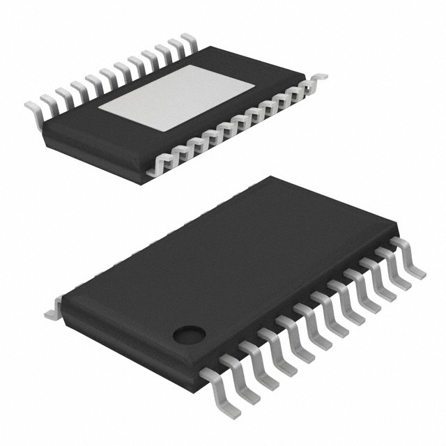
Thermally Enhanced 28-Lead TSSOP Package
The high switching frequency offers several advantages
by permitting the use of small inductors and ceramic
capacitors, leading to a very small triple output solution.
The constant switching frequency, combined with low
impedance ceramic capacitors, result in low, predictable
output ripple. With its wide input voltage range of 3.5V to
25V, the LT1941 regulates a broad array of power sources
from 4-cell batteries and 5V logic rails to unregulated wall
transformers, lead acid batteries and distributed-power
supplies.
APPLICATIONS
n
n
n
n
n
n
Cable Modems
DSL Modems
Distributed Power Regulation
Wall Transformer Regulation
Disk Drives
DSP Power
L, LT, LTC and LTM are registered trademarks of Linear Technology Corporation. All other
trademarks are the property of their respective owners.
TYPICAL APPLICATION
VOUT1
VIN
4.7V TO 14V
130k
100k
5GOOD
VIN
PGOOD1
PGOOD3
3300pF
7.32k
22μH
VOUT3
–12V
350mA*
10μF
3.3k
1.5nF
1μF
22μH
133k
0.22μF
SW1
SW2
FB1
FB2
VC1
VC2
SW3
BIAS1
NFB
BIAS2
10μF
3.3μH
VOUT2
3.3V
1.4A
10.7k
1000pF
10k
RUNSS1 RUNSS2
22μF
2.49k
1.5nF
FB3
RUNSS3
GND
1.5nF
RUN/SS
2V/DIV
VOUT1
2V/DIV
VOUT2
5V/DIV
VOUT3
10V/DIV
22nF
IVIN(AVE)
1A/DIV
PGOOD2
5V/DIV
VC3
13.7k
Start-Up Waveforms
with Sequencing
BOOST2
LT1941
13.7k
33μF
PGOOD1
12GOOD PGOOD3
0.22μF
3μH
100k
PGOOD2
BOOST1
VOUT1
1.8V
2.4A
100k
PGOOD2
5GOOD
12GOOD
100k
VOUT2
1.5k
2ms/DIV
1941 F01b
1941 F01
*240mA AT VIN = 5V, 550mA AT VIN = 12V
Figure 1. Triple Output Power Supply: 3.3V, 1.8V, –12V
1941fb
1
�LT1941
ABSOLUTE MAXIMUM RATINGS
PIN CONFIGURATION
(Note 1)
TOP VIEW
VIN Pin ........................................................(–0.3V), 25V
BOOST Pin Voltage ...................................................35V
BOOST Above SW Pin ...............................................25V
BIAS1, BIAS2 Pins ....................................................25V
PGOOD, 5GOOD, 12GOOD Pins.................................25V
RUN/SS, VC, FB, NFB Pins ..........................................3V
SW1, SW2 Voltage .....................................................VIN
SW3 Voltage .............................................................40V
Maximum Junction Temperature (Note 6) ............ 125°C
Operating Ambient Temperature Range
(Note 2)....................................................–40°C to 85°C
Storage Temperature Range .................. –65°C to 150°C
Lead Temperature (Soldering, 10 sec)................... 300°C
VIN
1
28 BIAS2
VIN
2
27 SW3
SW1
3
26 PGND
SW1
4
25 VIN
BOOST1
5
24 BOOST2
PGOOD1
6
23 SW2
VC1
7
FB1
8
PGOOD2
9
20 FB3
VC2 10
19 NFB
FB2 11
18 VC3
29
22 VIN
21 PGOOD3
RUN/SS1 12
17 5GOOD
RUN/SS2 13
16 12GOOD
RUN/SS3 14
15 BIAS1
FE PACKAGE
28-LEAD PLASTIC TSSOP
TJMAX = 125°C, θJA = 25°C/W
EXPOSED PAD (PIN 29) IS GND, MUST BE SOLDERED TO PCB
ORDER INFORMATION
LEAD FREE FINISH
TAPE AND REEL
PART MARKING
PACKAGE DESCRIPTION
TEMPERATURE RANGE
LT1941EFE#PBF
LT1941EFE#TRPBF
LT1941EFE
28-LEAD PLASTIC TSSOP
–40°C to 85°C
LEAD BASED FINISH
TAPE AND REEL
PART MARKING
PACKAGE DESCRIPTION
TEMPERATURE RANGE
LT1941EFE
LT1941EFE#TR
LT1941EFE
28-LEAD PLASTIC TSSOP
–40°C to 85°C
Consult LTC Marketing for parts specified with wider operating temperature ranges.
For more information on lead free part marking, go to: http://www.linear.com/leadfree/
For more information on tape and reel specifications, go to: http://www.linear.com/tapeandreel/
ELECTRICAL CHARACTERISTICS
The l denotes the specifications which apply over the full operating temperature
range, otherwise specifications are at TA = 25°C. VIN, VBIAS1, VBIAS2 = 5V, VBOOST1, VBOOST2 = 8V, unless otherwise noted. (Note 2)
PARAMETER
CONDITIONS
MIN
l
TYP
MAX
UNITS
3.3
3.5
V
VIN Quiescent Current
Not Switching
2
3.5
mA
BIAS1 Quiescent Current
Not Switching
5
7.5
mA
BIAS2 Quiescent Current
Not Switching
1.6
2.2
mA
Shutdown Current
VRUNSS1,2,3 = 0V
50
75
μA
Minimum Operating Voltage
Reference Voltage Line Regulation
5V < VIN < 25V
0.01
%/V
VC Source Current
VC = 0.6V
100
μA
VC Sink Current
VC = 0.6V
100
μA
VC Clamp Voltage
Switching Frequency
1.7
l
0.9
1.1
V
1.35
MHz
1941fb
2
�LT1941
ELECTRICAL CHARACTERISTICS
The l denotes the specifications which apply over the full operating temperature
range, otherwise specifications are at TA = 25°C. VIN, VBIAS1, VBIAS2 = 5V, VBOOST1, VBOOST2 = 8V, unless otherwise noted. (Note 2)
PARAMETER
CONDITIONS
MIN
TYP
MAX
UNITS
Switching Phase
SW1 to SW2
SW1 to SW3
150
–30
180
0
210
30
Deg
Deg
Foldback Frequency
VFB = 0V
200
RUN/SS Current
RUN/SS Threshold
1
2
0.4
kHz
3
μA
0.6
V
5GOOD Threshold
VIN Rising
4.5
V
5GOOD Voltage Output Low
I5GOOD = 125μA, VIN = 4V
0.2
0.4
V
5GOOD Leakage
V5GOOD = 2V
10
400
nA
12GOOD Threshold
VIN Rising
10.8
V
12GOOD Voltage Output Low
I12GOOD = 125μA
0.2
0.4
V
12GOOD Leakage
V12GOOD = 2V, VIN = 12V
10
400
nA
PGOOD Voltage Output Low
IPGOOD = 200μA
0.2
0.4
V
PGOOD Pin Leakage
VPGOOD = 2V
10
400
nA
628
638
638
mV
mV
50
500
nA
3A Step-Down
FB1 Voltage
l
l
FB1 Pin Bias Current
PGOOD1 Threshold Offset
618
613
VFB Rising
54
mV
Frequency Shift Threshold on FB1
0.35
V
Error Amplifier Transconductance
1700
μMhos
Error Amplifier Voltage Gain
500
V/V
VC Switching Threshold
0.9
V
VC1 to Switch Current Gain
5
Switch 1 Current Limit (Note 3)
VIN = 12V, VBOOST1, VBOOST2 = 15V
Switch 1 VCESAT (Note 7)
BOOST1 Pin Current
l
3
A/V
4.3
6
ISW = 2.5A
400
600
mV
ISW = 2.5A
40
60
mA
0.01
10
μA
1.8
2.5
Switch 1 Leakage Current
Minimum Boost Voltage Above Switch (Note 4)
Maximum Duty Cycle
l
78
88
l
618
613
628
638
638
50
500
A
V
%
2A Step-Down
FB2 Voltage
l
FB2 Pin Bias Current
PGOOD2 Threshold Offset
VFB Rising
54
mV
mV
nA
mV
Frequency Shift Threshold on FB2
0.35
V
Error Amplifier Transconductance
1700
μMhos
Error Amplifier Voltage Gain
500
V/V
VC Switching Threshold
0.9
V
VC2 to Switch Current Gain
3.6
A/V
Switch 2 Current Limit (Note 3)
VIN = 12V, VBOOST1, VBOOST2 = 15V
Switch 2 VCESAT (Note 7)
BOOST2 Pin Current
l
2
2.9
4.1
A
ISW = 1.5A
450
600
mV
ISW = 1.5A
26
40
mA
1941fb
3
�LT1941
ELECTRICAL CHARACTERISTICS
The l denotes the specifications which apply over the full operating temperature
range, otherwise specifications are at TA = 25°C. VIN, VBIAS1, VBIAS2 = 5V, VBOOST1, VBOOST2 = 8V, unless otherwise noted. (Note 2)
PARAMETER
CONDITIONS
MIN
Switch 2 Leakage Current
Minimum Boost Voltage Above Switch (Note 4)
Maximum Duty Cycle
TYP
MAX
0.01
10
UNITS
μA
1.8
2.5
V
l
78
88
l
1.23
1.22
1.25
1.27
1.27
V
V
800
1400
nA
%
1.5A Inverting/Boost
FB3 Voltage
FB3 Pin Bias Current
l
NFB Voltage
l
NFB Pin Bias Current
l
NFB3 Voltage (VFB3-VNFB)
–15
0
15
mV
60
500
nA
1.258
1.260
V
V
l
1.212
1.205
1.24
l
150
350
μA
120
mV
Error Amplifier Transconductance
800
μMhos
Error Amplifier Voltage Gain
150
V/V
VC Switching Threshold
1.1
V
FB3 Pin Output Current
VFB3 = 1.35V, VNFB = –0.1V
PGOOD3 Threshold Offset
VFB Rising
VC3 to Switch Current Gain
5
Frequency Shift Threshold on FB3
A/V
0.65
l
Switch 3 Current Limit (Note 5)
1.5
V
2
2.9
A
Switch 3 VCESAT
ISW = 1A
240
320
mV
BIAS2 Pin Current
ISW = 1A
30
45
mA
0.01
10
μA
Switch 3 Leakage Current
Maximum Duty Cycle
Note 1: Stresses beyond those listed under Absolute Maximum Ratings
may cause permanent damage to the device. Exposure to any Absolute
Maximum Rating condition for extended periods may affect device
reliability and lifetime.
Note 2: The LT1941E is guaranteed to meet performance specifications
from 0°C to 70°C. Specifications over the –40°C to 85°C operating
temperature range are assured by design, characterization and correlation
with statistical process controls.
Note 3: Current limit is guaranteed by design and/or correlation to static
test. Slope compensation reduces current limit at higher duty cycles.
l
77
86
%
Note 4: This is the minimum voltage across the boost capacitor needed to
guarantee full saturation of the internal power switch.
Note 5: Current limit is guaranteed by design and/or correlation to static
test.
Note 6: This IC includes overtemperature protection that is intended
to protect the device during momentary overload conditions. Junction
temperature will exceed 125°C when overtemperature protection is active.
Continuous operation above the specified maximum operating junction
temperature may impair device reliability.
Note 7: Guaranteed by design, not 100% tested.
1941fb
4
�LT1941
TYPICAL PERFORMANCE CHARACTERISTICS
Efficiency, VOUT1 = 1.8V
90
Efficiency, VOUT2 = 3.3V
90
VIN = 5V
TA = 25°C
70
60
60
0
0.5
1.5
1
LOAD CURRENT (A)
2
50
0
0.25
1.25
0.5
0.75
1
LOAD CURRENT (A)
600
100
400
300
200
0.5
1
1.5
2
SWITCH CURRENT (A)
2.5
0
3
0.5
1
1.5
SWITCH CURRENT (A)
0
1941 G02
SW1 Current Limit vs Duty Cycle
200
2.5
CURRENT LIMIT (A)
MINIMUM
2.5
2.0
1.5
1.0
0.25
0.5
0.75
1
1.25
SWITCH CURRENT (A)
TYPICAL
2.0
1.5
BOOST2 Pin Current
40
BOOST CURRENT (mA)
TYPICAL
3.5
0
1941 G10
SW2 Current Limit vs Duty Cycle
4.0
3.0
300
0
2
3.0
4.5
TA = 25°C
1941 G09
5.0
300
100
100
0
250
400
SWITCH VOLTAGE (mV)
SWITCH VOLTAGE (mV)
200
100
150
200
LOAD CURRENT (mA)
SW3 VCESAT
500
500
400
300
50
1941 G08
TA = 25°C
TA = 25°C
SWITCH VOLTAGE (mV)
0
SW2 VCESAT
SW1 VCESAT
500
CURRENT LIMIT (A)
1.5
1941 G07
1941 G01
0
70
60
50
2.5
VIN = 5V
TA = 25°C
80
EFFICIENCY (%)
70
50
VIN = 5V
TA = 25°C
80
EFFICIENCY (%)
EFFICIENCY (%)
80
Efficiency, VOUT3 = –12V
90
MINIMUM
1.5
1.0
TA = 25°C
30
20
10
0.5
0.5
0
0
0
20
60
40
DUTY CYCLE (%)
80
100
1941 G03
0
20
40
60
DUTY CYCLE (%)
80
100
1941 G06
0
0
1
1.5
0.5
SW2 PIN CURRENT (A)
2
1941 G11
1941fb
5
�LT1941
TYPICAL PERFORMANCE CHARACTERISTICS
BOOST1 Pin Current
VFB3 vs Temperature
TA = 25°C
BOOST CURRENT (mA)
40
0.645
1.265
0.635
VFB (V)
30
VFB1, VFB2 vs Temperature
1.280
VFB (V)
50
1.250
0.625
20
1.235
0.615
10
0
0.5
1
1.5
2
SW1 PIN CURRENT (A)
2.5
3
1.220
–50
–25
75
0
25
50
TEMPERATURE (°C)
100
1941 G04
1.2
1.1
1.0
100
TA = 25°C
0.8
0.6
0.4
0
20
40
60
80
% OF FEEDBACK VOLTAGE
1941 G13
8.0
1.2
7.5
MINIMUM INPUT VOLTAGE (V)
RUN/SS THRESHOLDS (V)
1.5
1.0
0
–50
100
1941 G14
1.0
TO SWITCH
0.8
0.6
TO RUN
0.4
0.2
100
125
1941 G16
7.0
6.5
BOOST DIODE
TIED TO
OUTPUT
BOOST DIODE
TIED TO
INPUT
6.0
VIN TO RUN
5.5
5.0
1
10
100
LOAD CURRENT (mA)
75
0
25
50
TEMPERATURE (°C)
100
125
Minimum Input Voltage
VOUT2 = 3.3V
6.0
DBOOST = CMDSH-3
TA = 25°C
VIN TO START
–25
1941 G15
Minimum Input Voltage
VOUT2 = 5V
1.4
50
25
75
0
TEMPERATURE (°C)
2.0
0.5
0.2
RUN/SS Thresholds
vs Temperature
125
2.5
1.0
125
100
IRUN/SS vs Temperature
0
75
0
25
50
TEMPERATURE (°C)
75
0
25
50
TEMPERATURE (°C)
3.0
RUN/SS CURRENT (μA)
SWITCHING FREQUENCY (MHz)
FREQUENCY (MHz)
1.2
–25
1941 G12
Switching Frequency
vs % of Feedback Voltage
1.3
0
–50 –25
0.605
–50
1941 G05
Frequency vs Temperature
0.9
–50 –25
125
1000
1941 G17
MINIMUM INPUT VOLTAGE (V)
0
DBOOST = CMDSH-3
TA = 25°C
5.5
VIN TO START
5.0
BOOST DIODE
TIED TO
OUTPUT
BOOST DIODE
TIED TO
INPUT
4.5
VIN TO RUN
4.0
3.5
3.0
1
10
100
LOAD CURRENT (mA)
1000
1941 G18
1941fb
6
�LT1941
PIN FUNCTIONS
VIN (Pins 1, 2, 22, 25): The VIN pins supply current to
the LT1941’s internal circuitry and to the internal power
switches. These pins must be tied to the same source and
locally bypassed.
BIAS1 (Pin 15): The BIAS1 pin supplies the current to
the LT1941’s internal regulator. Tie this pin to the lowest
available voltage source above 2.35V (Either VIN, VOUT or
any other available supply).
SW1, SW2, SW3 (Pins 3, 4, 23, 27): The SW pins are
the outputs of the internal power switches. Connect these
pins to the inductors and switching diodes.
12GOOD (Pin 16): The 12GOOD pin is the open-collector
output of an internal comparator. 12GOOD remains low until
VIN is within 10% of 12V. The pin pulls low when the part
is in shutdown. Leave this pin unconnected if unused.
BOOST1, BOOST2 (Pins 5, 24): The BOOST pins are used
to provide drive voltages, higher than the input voltage,
to the internal bipolar NPN power switches. Tie through
a diode from VOUT or from VIN.
PGOOD1, PGOOD2, PGOOD3 (Pins 6, 9, 21): The PGOOD
pins are the open-collector outputs of an internal comparator. PGOOD remains low until the FB pin is within 10% of
the final regulation voltage. As well as indicating output
regulation, the PGOOD pins can sequence the switching
regulators. Leave these pins unconnected if unused. The
PGOOD outputs are valid when VIN is greater than 3.5V
and any of the RUN/SS pins are high. They are not valid
when all RUN/SS pins are low.
VC1, VC2, VC3 (Pins 7, 10, 18): The VC pins are the outputs
of the internal error amps. The voltages on these pins
control the peak switch currents. These pins are normally
used to compensate the control loops. Each switching
regulator can be shut down by pulling its respective VC
pin to ground with an NMOS or NPN transistor.
FB1, FB2, FB3 (Pins 8, 11, 20): The LT1941 regulates each
feedback pin to either 0.628V (FB1, FB2) or 1.25V (FB3).
Connect the feedback resistor divider taps to these pins.
5GOOD (Pin 17): The 5GOOD pin is the open-collector
output of an internal comparator. 5GOOD remains low until
VIN is within 10% of 5V. The pin pulls low when the part is
in shutdown. Leave this pin unconnected if unused.
NFB (Pin 19): The LT1941 contains an op amp configured
with an output at FB3, noninverting terminal at GND and
an inverting terminal at NFB. Connect the feedback resistor
network virtual ground at this node if regulating negative
voltages. Otherwise, tie this node to FB3.
PGND (Pin 26): Tie directly to local ground plane.
BIAS2 (Pin 28): The BIAS2 pin supplies the current to
the driver of SW3. Tie this pin to the lowest available
voltage source above 2.5V (Either VIN, VOUT or any other
available supply).
Exposed Pad (Pin 29): Ground. The underside Exposed
Pad metal of the package provides both electrical contact
to ground and good thermal contact to the printed circuit
board. The Exposed Pad must be soldered to the circuit
board ground for proper operation.
RUN/SS1, RUN/SS2, RUN/SS3 (Pins 12, 13, 14): The
RUN/SS pins are used to shut down the individual switching
regulators and the internal bias circuits. They also provide
a soft-start function. To shut down either regulator, pull
the RUN/SS pin to ground with an open drain or collector. Tie a capacitor from this pin to ground to limit switch
current during start-up. If neither feature is used, leave
these pins unconnected.
1941fb
7
�LT1941
BLOCK DIAGRAM
The LT1941 is a constant frequency, current mode, triple
output regulator with internal power switches. The three
regulators share common circuitry including input source,
voltage reference and oscillator, but are otherwise independent. Operation can be best understood by referring
to the Block Diagram.
If the RUN/SS pins are tied to ground, the LT1941 is shut
down and draws 50μA from the input source tied to VIN.
Internal 2μA current sources charge external soft-start
capacitors, generating voltage ramps at these pins. If any
of the RUN/SS pins exceed 0.6V, the internal bias circuits
turn on, including the internal regulator, reference and
1.1MHz master oscillator. Each switching regulator will
only begin to operate when its corresponding RUN/SS pin
reaches ≈1V. The master oscillator generates three clock
signals, with the two signals for the step-down regulators
out of phase by 180°.
The three switchers are current mode regulators. Instead
of directly modulating the duty cycle of the power switch,
the feedback loop controls the peak current in the switch
during each cycle. Compared to voltage mode control, current mode control improves loop dynamics and provides
cycle-by-cycle current limit.
The Block Diagram shows only one of the two step-down
switching regulators. A pulse from the slave oscillator
sets the RS flip-flop and turns on the internal NPN bipolar power switch. Current in the switch and the external
inductor begins to increase. When this current exceeds a
level determined by the voltage at VC, current comparator
C1 resets the flip-flop, turning off the switch. The current
in the inductor flows through the external Schottky diode
and begins to decrease. The cycle begins again at the next
pulse from the oscillator. In this way, the voltage on the
VC pin controls the current through the inductor to the
output. The internal error amplifier regulates the output
voltage by continually adjusting the VC pin voltage. The
threshold for switching on the VC pin is ≈1V and an active
clamp of 1.7V limits the output current. The RUN/SS pin
voltage also clamps the VC pin voltage. As the internal
current source charges the external soft-start capacitor,
the current limit increases slowly. An internal op amp
allows the part to regulate negative voltages using only
two external resistors.
Each switcher contains an extra, independent oscillator to
perform frequency foldback during overload conditions.
This slave oscillator is normally synchronized to the master
oscillator. A comparator senses when VFB is less than 50%
of its regulated value and switches the regulator from the
master oscillator to a slower slave oscillator. The VFB pin is
less than 50% of its regulated value during start-up, short
circuit and overload conditions. Frequency foldback helps
limit switch current under these conditions.
The switch drivers for SW1 and SW2 operate either
from VIN or from the BOOST pin. An external capacitor
and diode are used to generate a voltage at the BOOST
pin that is higher than the input supply. This allows the
driver to saturate the internal bipolar NPN power switch
for efficient operation.
The BIAS1 pin allows the internal circuitry to draw its
current from a lower voltage supply than the input, also
reducing power dissipation and increasing efficiency. If
the voltage on the BIAS1 pin falls below 2.35V, then its
quiescent current will flow from VIN.
The BIAS2 pin allows the driver for SW3 to draw its
current from a lower voltage supply than the input. This
reduces power dissipation within the part and increases
efficiency. If the voltage on the BIAS2 pin falls below ≈2V,
then SW3 will lock out and will not be able to turn on until
BIAS2 rises above ≈2.1V.
A power good comparator trips when the FB pin is at
91% of its regulated value. The PGOOD output is an
open-collector transistor that is off when the output is in
regulation, allowing an external resistor to pull the PGOOD
pin high. Power good is valid when the LT1941 is enabled
and VIN > 3.5V.
Input power good comparators monitor the input supply.
The 5GOOD and 12GOOD pins are open-collector outputs
of internal comparators. The 5GOOD pin remains low until
the input is within 10% of 5V. The 12GOOD pin remains
low until the input is within 10% of 12V. The 5GOOD and
12GOOD pins are valid as long as VIN is greater than
1.1V. Both the 5GOOD and 12GOOD pins will sink current
when the part is in shutdown, independent of the voltage
at VIN.
1941fb
8
�LT1941
BLOCK DIAGRAM
VIN
5GOOD
+
BIAS1
VIN
RUN/SS1
4.5V
2μA
INT REG
AND REF
One of Two Step-Down Switching Regulators
RUN/SS2
RUN/SS3
CLK1
CLK2
CLK3
MASTER
OSC
–
12GOOD
+
2μA
10.8V
–
VIN
2μA
VIN
CIN
+
0.9V
–
+
¤
BOOST
SLOPE
–
S
C1
SLAVE
OSC
CLK
D2
R
Q
C3
SW
L1
OUT
+
–
0.35V
FB
R1
–
VC
ERROR
AMP
RC
–
RUN/SS
CC
+
CF
C1
D1
ILIMIT
CLAMP
+
R2
0.628V
54mV
1.7V
PGOOD
+
GND
–
VIN
BIAS2
BOOST
VC3
L3
SW3
–
RUN/SS
C2
VOUT3
DRIVER
C4
Q1
R S Q
+
ERROR
AMP
FB3
FB3
NFB
0.4V
L4A
–VOUT3
SW3
+
–
C5
D4
C6
SLAVE
OSCILLATOR
CLK3
+
R3
(EXTERNAL)
NFB
R4
(EXTERNAL)
0.6V
NFB
–VOUT3
INVERTING
PGND
L4B
FB3
FOR
NEGATIVE
OUTPUTS
VIN
0.01Ω
RAMP
GENERATOR
R3
(EXTERNAL)
R4
(EXTERNAL)
3
–
VOUT3
FOR
POSITIVE
OUTPUTS
+
–
1.25V
+
Inverting/Boost Switching Regulator
D3
SW3
–
–
+
PGOOD3
+
1.12V
–
1941 F02
Figure 2. Block Diagram of the LT1941 with Associated External Components
1941fb
9
�LT1941
APPLICATIONS INFORMATION
STEP-DOWN CONSIDERATIONS
FB Resistor Network
The output voltage is programmed with a resistor divider
(refer to the Block Diagram) between the output and the
FB pin. Choose the resistors according to
R1 = R2(VOUT/628mV – 1)
R2 should be 10k or less to avoid bias current errors.
Input Voltage Range
The minimum operating voltage is determined either by the
LT1941’s undervoltage lockout of ~3.3V or by its maximum
duty cycle. The duty cycle is the fraction of time that the
internal switch is on and is determined by the input and
output voltages:
DC = (VOUT + VF)/(VIN – VSW + VF)
where VF is the forward voltage drop of the catch diode
(~0.4V) and VSW is the voltage drop of the internal switch
(~0.3V at maximum load). This leads to a minimum input
voltage of:
VIN(MIN) = (VOUT + VF)/DCMAX – VF + VSW
with DCMAX = 0.78.
The maximum operating voltage is determined by the
absolute maximum ratings of the VIN and BOOST pins
and by the minimum duty cycle DCMIN = 0.15:
VIN(MAX) = (VOUT + VF)/DCMIN – VF + VSW
This limits the maximum input voltage to ~14V with
VOUT = 1.8V and ~19V with VOUT = 2.5. Note that this is
a restriction on the operating input voltage; the circuit
will tolerate input voltage transients up to the Absolute
Maximum Rating.
Inductor Selection and Maximum Output Current
A good first choice for the inductor value is
where VF is the voltage drop of the catch diode (~0.4V) and
L is in μH. With this value the maximum load current will
be 2.1A for SW1 and 1.4A for SW2, independent of input
voltage. The inductor’s RMS current rating must be greater
than the maximum load current and its saturation current
should be at least 30% higher. For highest efficiency, the
series resistance (DCR) should be less than 0.1Ω. Table 1
lists several vendors and types that are suitable.
Table 1. Inductors
VALUE
(μH)
ISAT
(A)
DCR
(Ω)
HEIGHT
(mm)
CR43-1R4
1.4
2.52
0.056
3.5
CR43-2R2
2.2
1.75
0.071
3.5
CDRH3D16-1R5
1.5
1.55
0.040
1.8
CDRH4D28-3R3
3.3
1.57
0.049
3.0
CDRH4D18-1R0
1.0
1.70
0.035
2.0
CDC5D23-2R2
2.2
2.50
0.03
2.5
CDRH5D28-2R6
2.6
2.60
0.013
3.0
DO1606T-152
1.5
2.10
0.060
2.0
DO1606T-222
2.2
1.70
0.070
2.0
DO1608C-152
1.5
2.60
0.050
2.9
DO1608C-222
2.2
2.30
0.070
2.9
DO1608C-332
3.3
2.00
0.080
2.9
DO1608C-472
4.7
1.50
0.090
2.9
MOS6020-222
2.2
2.15
0.035
2.0
MOS6020-332
3.3
1.8
0.046
2.0
PART NUMBER
Sumida
Coilcraft
MOS6020-472
4.7
1.5
0.050
2.0
DO3314-222
2.2
1.6
0.200
1.4
(D62F)847FY-2R4M
2.4
2.5
0.037
2.7
(D73LF)817FY-2R2M
2.2
2.7
0.03
3.0
Toko
The optimum inductor for a given application may differ
from the one indicated by this simple design guide. A
larger value inductor provides a slightly higher maximum
load current and will reduce the output voltage ripple. If
L = (VOUT + VF)/1.6 for SW1
L = (VOUT + VF)/1.1 for SW2
1941fb
10
�LT1941
APPLICATIONS INFORMATION
your load is lower than the maximum load current, then
you can relax the value of the inductor and operate with
higher ripple current. This allows you to use a physically
smaller inductor or one with a lower DCR resulting in
higher efficiency. Be aware that if the inductance differs
from the simple rule above, then the maximum load current
will depend on input voltage. In addition, low inductance
may result in discontinuous mode operation, which further
reduces maximum load current. For details of maximum
output current and discontinuous mode operation, see
Linear Technology’s Application Note AN44. Finally, for
duty cycles greater than 50% (VOUT/VIN > 0.5), a minimum
inductance is required to avoid subharmonic oscillations.
See AN19.
The current in the inductor is a triangle wave with an average
value equal to the load current. The peak switch current
is equal to the output current plus half the peak-to-peak
inductor ripple current. The LT1941 limits its switch current in order to protect itself and the system from overload
faults. Therefore, the maximum output current that the
LT1941 will deliver depends on the switch current limit,
the inductor value and the input and output voltages.
When the switch is off, the potential across the inductor
is the output voltage plus the catch diode drop. This gives
the peak-to-peak ripple current in the inductor:
ΔIL = (1 – DC)(VOUT + VF)/(L • f)
where f is the switching frequency of the LT1941 and L
is the value of the inductor. The peak inductor and switch
current is:
ISWPK = ILPK = IOUT + ΔIL/2
To maintain output regulation, this peak current must be
less than the LT1941’s switch current limit ILIM. For SW1,
ILIM is at least 3A at low duty cycles and decreases linearly
to 2.4A at DC = 0.8. For SW2, ILIM is at least 2A for at low
duty cycles and decreases linearly to 1.6A at DC = 0.8.
The maximum output current is a function of the chosen
inductor value:
IOUT(MAX) = ILIM – ΔIL/2
= 3 • (1 – 0.25 • DC) – ΔIL/2 for SW1
= 2 • (1 – 0.25 • DC) – ΔIL/2 for SW2
Choosing an inductor value so that the ripple current is
small will allow a maximum output current near the switch
current limit.
One approach to choosing the inductor is to start with the
simple rule given above, look at the available inductors
and choose one to meet cost or space goals. Then use
these equations to check that the LT1941 will be able to
deliver the required output current. Note again that these
equations assume that the inductor current is continuous. Discontinuous operation occurs when IOUT is less
than ΔIL/2.
Output Capacitor Selection
For 5V and 3.3V outputs, a 10μF, 6.3V ceramic capacitor
(X5R or X7R) at the output results in very low output voltage ripple and good transient response. For lower voltages,
10μF is adequate for ripple requirements but increasing
COUT will improve transient performance. Other types and
values will also work; the following discusses tradeoffs in
output ripple and transient performance.
The output capacitor filters the inductor current to generate
an output with low voltage ripple. It also stores energy in
order to satisfy transient loads and stabilize the LT1941’s
control loop. Because the LT1941 operates at a high
frequency, minimal output capacitance is necessary. In
addition, the control loop operates well with or without
the presence of output capacitor series resistance (ESR).
Ceramic capacitors, which achieve very low output ripple
and small circuit size, are therefore an option.
1941fb
11
�LT1941
APPLICATIONS INFORMATION
You can estimate output ripple with the following
equations:
VRIPPLE = ΔIL/(8 • f • COUT) for ceramic capacitors
and
Table 2. Low ESR Surface Mount Capacitors
VENDOR
TYPE
SERIES
Taiyo-Yuden
Ceramic
AVX
Ceramic
Tantalum
TPS
VRIPPLE = ΔIL • ESR for electrolytic capacitors (tantalum
and aluminum)
Kemet
Tantalum
Tantalum Organic
Aluminum Organic
T491,T494,T495
T520
A700
where ΔIL is the peak-to-peak ripple current in the inductor.
The RMS content of this ripple is very low so the RMS
current rating of the output capacitor is usually not of
concern. It can be estimated with the formula:
Sanyo
Tantalum or Aluminum Organic
POSCAP
Aluminum Organic
SP CAP
IC(RMS) = ΔIL/√12
Another constraint on the output capacitor is that it must
have greater energy storage than the inductor; if the stored
energy in the inductor transfers to the output, the resulting
voltage step should be small compared to the regulation
voltage. For a 5% overshoot, this requirement indicates:
COUT > 10 • L • (ILIM/VOUT)2
The low ESR and small size of ceramic capacitors make
them the preferred type for LT1941 applications. Not all
ceramic capacitors are the same, however. Many of the
higher value capacitors use poor dielectrics with high
temperature and voltage coefficients. In particular, Y5V
and Z5U types lose a large fraction of their capacitance
with applied voltage and at temperature extremes.
Because loop stability and transient response depend on
the value of COUT, this loss may be unacceptable. Use
X7R and X5R types.
Electrolytic capacitors are also an option. The ESRs of
most aluminum electrolytic capacitors are too large to
deliver low output ripple. Tantalum, as well as newer,
lower-ESR organic electrolytic capacitors intended for
power supply use are suitable. Chose a capacitor with a
low enough ESR for the required output ripple. Because
the volume of the capacitor determines its ESR, both the
size and the value will be larger than a ceramic capacitor
that would give similar ripple performance. One benefit
is that the larger capacitance may give better transient
response for large changes in load current. Table 2 lists
several capacitor vendors.
Panasonic
TDK
Ceramic
Diode Selection
The catch diode (D1 from Figure 2) conducts current only
during switch off time. Average forward current in normal
operation can be calculated from:
ID(AVG) = IOUT (VIN – VOUT)/VIN
The only reason to consider a diode with a larger current
rating than necessary for nominal operation is for the
worst-case condition of shorted output. The diode current
will then increase to the typical peak switch current.
Peak reverse voltage is equal to the regulator input voltage.
Use a diode with a reverse voltage rating greater than the
input voltage. Table 3 lists several Schottky diodes and
their manufacturers.
Table 3. Schottky Diodes
PART
NUMBER
VR
(V)
IAVE
(A)
VF AT 1A
(mV)
VF AT 2A
(mV)
On Semiconductor
MBRM120E
MBRM140
20
40
1
1
530
550
595
Diodes Inc.
B120
B130
B220
B230
20
30
20
30
1
1
2
2
500
500
International Rectifier
10BQ030
20BQ030
30
30
1
2
420
500
500
470
470
1941fb
12
�LT1941
APPLICATIONS INFORMATION
Boost Pin Considerations
The capacitor and diode tied to the BOOST pin generate
a voltage that is higher than the input voltage. In most
cases, a 0.18μF capacitor and fast switching diode (such
as the CMDSH-3 or MMSD914LT1) will work well. Figure 3
shows four ways to arrange the boost circuit. The BOOST
pin must be more than 2.5V above the SW pin for full
efficiency. For outputs of 3.3V and higher, the standard
circuit (Figure 3a) is best. For outputs between 2.8V and
3.3V, use a small Schottky diode (such as the BAT-54).
For lower output voltages, the boost diode can be tied to
the input (Figure 3b). The circuit in Figure 3a is more ef
ficient because the boost pin current comes from a lower
voltage source. Finally, as shown in Figure 3c, the anode
of the boost diode can be tied to another source that is
at least 3V. For example, if you are generating 3.3V and
1.8V and the 3.3V is on whenever the 1.8V is on, the 1.8V
boost diode can be connected to the 3.3V output. In any
case, be sure that the maximum voltage at the BOOST pin
is less than 35V and the voltage difference between the
BOOST and SW pins is less than 25V.
The boost circuit can also run directly from a DC voltage
that is higher than the input voltage by more than 2.5V + VF,
as in Figure 3d. The diode prevents damage to the LT1941
in case VIN2 is held low while VIN is present. The circuit
saves several components (both BOOST pins can be tied
to D2). However, efficiency may be lower and dissipation
in the LT1941 may be higher. Also, if VIN2 is absent the
LT1941 will still attempt to regulate the output, but will
do so with low efficiency and high dissipation because
the switch will not be able to saturate, dropping 1.5V to
2V in conduction.
The minimum operating voltage of an LT1941 application
is limited by the undervoltage lockout (3.5V) and by the
maximum duty cycle. The boost circuit also limits the
minimum input voltage for proper start-up. If the input
voltage ramps slowly, or the LT1941 turns on when the
output is already in regulation, the boost capacitor may
not be fully charged. Because the boost capacitor charges
with the energy stored in the inductor, the circuit will rely
on some minimum load current to get the boost circuit
running properly. This minimum load will depend on input
and output voltages, and on the arrangement of the boost
circuit. The minimum load current generally goes to zero
once the circuit has started. Even without an output load
current, in many cases the discharged output capacitor will
present a load to the switcher that will allow it to start.
D2
D2
C3
BOOST
LT1941
LT1941
VIN
VIN
VOUT
SW
VIN
VIN
SW
VBOOST – VSW VIN
MAX VBOOST 2VIN
VBOOST – VSW VOUT
MAX VBOOST VIN + VOUT
(3b)
(3a)
D2
D2
VIN2
>VIN + 3V
VIN2 > 3V
BOOST
BOOST
C3
LT1941
VIN
VOUT
GND
GND
VIN
C3
BOOST
LT1941
SW
VOUT
VIN
VIN
GND
SW
VOUT
GND
VBOOST – VSW VIN2
MAX VBOOST VIN2 + VIN
MINIMUM VALUE FOR VIN2 = 3V
MAX VBOOST – VSW VIN2
MAX VBOOST VIN2
MINIMUM VALUE FOR VIN2 = VIN + 3V
(3c)
1941 F03
(3d)
Figure 3. Generating the Boost Voltage
1941fb
13
�LT1941
APPLICATIONS INFORMATION
Converter with Backup Output Regulator
Regulating Negative Output Voltages
There is another situation to consider in systems where the
output will be held high when the input to the LT1941 is
absent. If the VIN and one of the RUN/SS pins are allowed
to float, then the LT1941’s internal circuitry will pull its
quiescent current through its SW pin. This is acceptable if
the system can tolerate a few mA of load in this state. With
both RUN/SS pins grounded, the LT1941 enters shutdown
mode and the SW pin current drops to ~50mA. However, if
the VIN pin is grounded while the output is held high, then
parasitic diodes inside the LT1941 can pull large currents
from the output through the SW pin and the VIN pin. A
Schottky diode in series with the input to the LT1941, as
shown in Figure 4, will protect the LT1941 and the system
from a shorted or reversed input.
The LT1941 contains an inverting op-amp with its noninverting terminal tied to ground and its output connected
to the FB3 pin. Use this op-amp to generate a voltage at
FB3 that is proportional to VOUT. Choose the resistors
according to:
R4 =
R3 • VOUT
1.24V
–VOUT
R4
R3
NFB
FB3
1941 AI02
PARASITIC DIODE
D4
VIN
Use 10k or larger, up to 20k for R3.
VIN
SW
VOUT
LT1941
1941 F04
Figure 4. Diode D4 Prevents a Shorted Input from
Discharging a Backup Battery Tied to the Output
INVERTER/BOOST CONSIDERATIONS
Regulating Positive Output Voltages
The output voltage is programmed with a resistor divider
between the output and the FB pin. Choose the resistors
according to:
⎛ V
⎞
R3 = R4 ⎜ OUT – 1⎟
⎝ 1.25V ⎠
Duty Cycle Range
The maximum duty cycle (DC) of the LT1941 inverter/boost
regulator is 77%. The duty cycle for a given application
using the inverting topology is:
DC =
VOUT
VIN + VOUT
The duty cycle for a given application using the boost
topology is:
V
–V
DC = OUT IN
VOUT
The LT1941 can still be used in applications where the
DC, as calculated above, is above 77%; however, the part
must be operated in discontinuous mode so that the actual
duty cycle is reduced.
R4 should be 10k or less to avoid bias current errors.
Inductor Selection
NFB should be tied to FB3.
VOUT
R3
R4
FB3
Several inductors that work well with the LT1941 inverter/
boost regulator are listed in Table 4. Besides these, many
other inductors will work. Consult each manufacturer
for detailed information and for their entire selection of
related parts. Use ferrite core inductors to obtain the best
efficiency. When using coupled inductors, choose one that
1941 AI01
1941fb
14
�LT1941
APPLICATIONS INFORMATION
can handle at least 1.5A of current without saturating and
ensure that the inductor has a low DCR (copper-wire resistance) to minimize I2R power losses. If using uncoupled
inductors, each inductor need only handle one-half of the
total switch current so that 0.75A per inductor is sufficient.
A 4.7μH to 15μH coupled inductor or two 15μH to 20μH
uncoupled inductors will usually be the best choice for
most LT1941 inverter designs. A 4.7μH to 15μH inductor
will be the best choice for most LT1941 boost designs. In
this case, the single inductor must carry the entire 1.5A
peak switch current.
Table 4. Inductors
VALUE
(μH)
ISAT(DC)
(A)
DCR
(Ω)
HEIGHT
(mm)
TP3-4R7
4.7
1.5
0.181
2.2
TP4-100
10
1.5
0.146
3.0
CDRH6D38NP-6R2
6.2
2.5
20m
3.8
CDRH6D38NP-7R4
7.4
2.3
23m
3.8
CDRH6D38NP-100
10
2.0
28m
3.8
PART NUMBER
Coiltronics
Sumida
Output Capacitor Selection
Use low ESR (equivalent series resistance) capacitors at
the output to minimize the output ripple voltage. Multilayer
ceramic capacitors are an excellent choice; they have an
extremely low ESR and are available in very small packages. X7R dielectrics are preferred, followed by X5R, as
these materials retain their capacitance over wide voltage
and temperature ranges. A 4.7μF to 20μF output capacitor
is sufficient for most LT1941 applications. Solid tantalum
or OS-CON capacitors will work but they will occupy more
board area and will have a higher ESR than a ceramic
capacitor. Always use a capacitor with a sufficient voltage rating.
Diode Selection
A Schottky diode is recommended for use with the LT1941
inverter/boost regulator. The Microsemi UPS120 is a very
good choice. Where the input to output voltage differential
exceeds 20V, use the UPS140 (a 40V diode). These diodes
are rated to handle an average forward current of 1A. For
applications where the average forward current of the
diode is less than 0.5A, use an ON Semiconductor
MBR0520L diode. The load current for boost, SEPIC and
inverting configurations is equal to the average diode
current.
BIAS2 Pin Considerations
The BIAS2 pin provides the drive current for the inverter/
boost switch. The voltage source on the BIAS2 line should
be able to supply the rated current and be at a minimum
of 2.5V. For highest efficiency, use the lowest voltage
source possible (VOUT = 3.3V, for example) to minimize
the VBIAS2 • IBIAS2 power loss inside the part.
INPUT CAPACITOR SELECTION
Bypass the input of the LT1941 circuit with a 10μF or
higher ceramic capacitor of X7R or X5R type. A lower
value or a less expensive Y5V type will work if there is
additional bypassing provided by bulk electrolytic capacitors, or if the input source impedance is low. The following
paragraphs describe the input capacitor considerations
in more detail.
Step-down regulators draw current from the input supply in pulses with very fast rise and fall times. The input
capacitor is required to reduce the resulting voltage ripple
at the LT1941 input and to force this switching current
into a tight local loop, minimizing EMI. The input capacitor must have low impedance at the switching frequency
to do this effectively and it must have an adequate ripple
current rating. With two switchers operating at the same
frequency but with different phases and duty cycles, calculating the input capacitor RMS current is not simple;
however, a conservative value is the RMS input current
for the channel that is delivering the most power (VOUT
times IOUT):
CIN(RMS) = IOUT •
VOUT ( VIN – VOUT )
VIN
<
IOUT
2
1941fb
15
�LT1941
APPLICATIONS INFORMATION
and is largest when VIN = 2 VOUT (50% duty cycle). As
the second, lower power channel draws input current, the
input capacitor’s RMS current actually decreases as the
out-of-phase current cancels the current drawn by the
higher power channel. The ripple current contribution
from the third channel will be minimal. Considering that
the maximum load current from a single channel is ~2.8A,
RMS ripple current will always be less than 1.4A.
The high frequency of the LT1941 reduces the energy
storage requirements of the input capacitor, so that the
capacitance required is often less than 10μF. The combination of small size and low impedance (low equivalent
series resistance or ESR) of ceramic capacitors makes
them the preferred choice. The low ESR results in very
low voltage ripple. Ceramic capacitors can handle larger
magnitudes of ripple current than other capacitor types
of the same value. Use X5R and X7R types.
An alternative to a high value ceramic capacitor is a lower
value along with a larger electrolytic capacitor, for example
a 1μF ceramic capacitor in parallel with a low ESR tantalum
capacitor. For the electrolytic capacitor, a value larger than
10μF will be required to meet the ESR and ripple current
requirements. Because the input capacitor is likely to see
high surge currents when the input source is applied, tantalum capacitors should be surge rated. The manufacturer
may also recommend operation below the rated voltage
of the capacitor. Be sure to place the 1μF ceramic as close
as possible to the VIN and GND pins on the IC for optimal
noise immunity.
A final caution is in order regarding the use of ceramic
capacitors at the input. A ceramic input capacitor can
combine with stray inductance to form a resonant tank
circuit. If power is applied quickly (for example by plugging
the circuit into a live power source), this tank can ring,
doubling the input voltage and damaging the LT1941. The
solution is to either clamp the input voltage or dampen the
tank circuit by adding a lossy capacitor in parallel with the
ceramic capacitor. For details, see Application Note 88.
Frequency Compensation
The LT1941 uses current mode control to regulate the
output. This simplifies loop compensation. In particular, the
LT1941 does not depend on the ESR of the output capacitor
for stability so you are free to use ceramic capacitors to
achieve low output ripple and small circuit size.
The components tied to the VC pin provide frequency
compensation. Generally, a capacitor and a resistor in
series to ground determine loop gain. In addition, there
is a lower value capacitor in parallel. This capacitor filters
noise at the switching frequency and is not part of the
loop compensation.
Loop compensation determines the stability and transient
performance. Designing the compensation network is a bit
complicated and the best values depend on the application
and the type of output capacitor. A practical approach is to
start with one of the circuits in this data sheet that is similar
to your application and tune the compensation network
to optimize the performance. Check stability across all
operating conditions, including load current, input voltage
and temperature. The LT1375 data sheet contains a more
thorough discussion of loop compensation and describes
how to test the stability using a transient load. Application
Note 76 is an excellent source as well.
Figure 5 shows an equivalent circuit for the LT1941 control
loop. The error amp is a transconductance amplifier with
finite output impedance. The power section, consisting of
the modulator, power switch and inductor is modeled as
a transconductance amplifier generating an output current proportional to the voltage at the VC pin. Note that
the output capacitor integrates this current and that the
capacitor on the VC pin (CC) integrates the error amplifier output current, resulting in two poles in the loop. In
most cases, a zero is required and comes either from the
output capacitor ESR or from a resistor in series with CC.
This model works well as long as the inductor current
ripple is not too low (ΔIRIPPLE > 5% IOUT ) and the loop
crossover frequency is less than ƒSW/5. A phase lead
capacitor (CPL) across the feedback divider may improve
the transient response.
The equivalent circuit for the LT1941 inverter control loop
is slightly different than is shown in Figure 5. The feedback
resistors are connected as shown for negative outputs in
Figure 2. The operational amplifier is fast enough to have
minimal effect on the loop dynamics.
1941fb
16
�LT1941
APPLICATIONS INFORMATION
Table 5. Converter Equivalent Model Parameters
STEP-DOWN1 STEP-DOWN2
BOOST
INVERTER
VFB
0.628V
0.628V
1.25
1.24
RO
500kΩ
500kΩ
500kΩ
500kΩ
gma
1700μmho
1700μmho
800μmho
800μmho
gmp
5mho
3.6mho
VIN • 5mho
VOUT
VIN • 5mho
–|VOUT|
LT1941
VSW
ERROR
AMPLIFIER
FB
+
VFB
gma
500k
GND
VC
RC
OUTPUT
R1
–
CURRENT MODE
POWER STAGE
gmp
CPL
ESR
C1
+
C1
CF
POLYMER
R2
OR
TANTALUM
CERAMIC
CC
1941 F05
Figure 5. Model for Loop Response
SOFT-START AND SHUTDOWN
single capacitor providing soft-start. The internal current
sources will charge these pins to ~2V.
The RUN/SS pins provide a soft-start function that limits
peak input current to the circuit during start-up. This helps
to avoid drawing more current than the input source can
supply or glitching the input supply when the LT1941 is
enabled. The RUN/SS pins do not provide an accurate
delay to start or an accurately controlled ramp at the
output voltage, both of which depend on the output capacitance and the load current. However, the power good
indicators can be used to sequence the three outputs, as
described below.
POWER GOOD INDICATORS
The PGOOD pin is the open-collector output of an internal
comparator. PGOOD remains low until the FB pin is within
10% of the final regulation voltage. Tie the PGOOD to any
supply with a pull-up resistor that will supply less than
200μA. Note that this pin will be open when the LT1941
is in shutdown mode (all three RUN/SS pins at ground)
regardless of the voltage at the FB pin. PGOOD is valid
when the LT1941 is enabled (any RUN/SS pin is high) and
VIN is greater than ~3.5V.
The RUN/SS (Run/Soft-Start) pins are used to place the
individual switching regulators and the internal bias circuits in shutdown mode. They also provide a soft-start
function. To shut down a regulator, pull its RUN/SS pin to
ground with an open drain or collector. If all three RUN/SS
pins are pulled to ground, the LT1941 enters its shutdown
mode with all regulators off and quiescent current reduced
to ~50mA. Internal 2μA current sources pull up on each
pin. If any RUN/SS pin reaches ~0.6V, the internal bias
circuits start and the quiescent currents increase to their
nominal levels.
The 5GOOD and 12GOOD pins are also open-collector
outputs of internal comparators. The 5GOOD pin remains
low until the input is within 10% of 5V. Tie the 5GOOD and
12GOOD pins to any supply with a pull-up resistor that will
supply less than 100μA. The 12GOOD pin remains low until
the input is within 10% of 12V. The 5GOOD and 12GOOD
pins are valid as long as VIN is greater than 1.1V. Both the
5GOOD and 12GOOD pins will sink current when the part
is in shutdown, independent of the voltage at VIN.
If a capacitor is tied from the RUN/SS pin to ground, then
the internal pull-up current will generate a voltage ramp on
this pin. This voltage clamps the VC pin, limiting the peak
switch current and therefore input current during start-up.
A good value for the soft-start capacitor is COUT/10,000,
where COUT is the value of the output capacitor.
The PG and RUN/SS pins can be used to sequence the
three outputs. Figure 6 shows several circuits to do this.
The techniques shown to sequence two channels can be
extended to sequence the third. In each case channel 1
starts first. Note that these circuits sequence the outputs
during start-up. When shut down the three channels turn
off simultaneously.
The RUN/SS pins can be left floating if the shutdown
feature is not used. They can also be tied together with a
Output Sequencing
1941fb
17
�LT1941
APPLICATIONS INFORMATION
In Figure 6a, a larger capacitor on RUN/SS2 delays channel
2 with respect to channel 1. The soft-start capacitor on
RUN/SS2 should be at least twice the value of the capacitor
on RUN/SS1. A larger ratio may be required, depending
on the output capacitance and load on each channel. Make
sure to test the circuit in the system before deciding on
final values for these capacitors.
The circuit in Figure 6b requires the fewest components,
with both channels sharing a single soft-start capacitor.
The power good comparator of channel 1 disables channel 2 until output 1 is in regulation.
For independent control of channel 2, use the circuit in
Figure 6c. The capacitor on RUN/SS1 is smaller than the
capacitor on RUN/SS2. This allows the LT1941 to start up
and enable its power good comparator before RUN/SS2
gets high enough to allow channel 2 to start switching.
Channel 2 only operates when it is enabled with the external
control signals and output 1 is in regulation.
The circuit in Figure 6a leaves both power good indicators free. However, the circuits in Figures 6b and 6c have
another advantage. As well as sequencing the two outputs
at start-up, they also disable channel 2 if output 1 falls
out of regulation (due to a short circuit or a collapsing
input voltage).
Finally, be aware that the circuit in Figure 6d does not
work, because the power good comparators are disabled
in shutdown.
PCB LAYOUT
For proper operation and minimum EMI, care must be taken
during printed circuit board (PCB) layout. Figure 7 shows
the high current paths in the step-down regulator circuit.
Note that in the step-down regulators large, switched
currents flow in the power switch, the catch diode and
the input capacitor. In the inverter/boost regulator large,
switched currents flow through the power switch, the
switching diode, and either the output capacitor in boost
configuration, or the tank capacitor in the inverter configuration. The loop formed by these components should
be as small as possible. Place these components, along
with the inductor and output capacitor, on the same side
of the circuit board and connect them on that layer. Place
a local, unbroken ground plane below these components
and tie this ground plane to system ground at one location, ideally at the ground terminal of the output capacitor
C2. Additionally, keep the SW and BOOST nodes as small
as possible.
RUN/SS1
RUN/SS1
OFF ON
1nF
OFF ON
VC2
1nF
LT1941
LT1941
RUN/SS2
GND
RUN/SS2 PG1
GND
2.2nF
(6a) Channel 2 is Delayed
(6b) Fewest Components
RUN/SS1
OFF ON
OFF2 ON2
LT1941
1nF
RUN/SS1
OFF ON
LT1941
1nF
PG1
PG1
RUN/SS2
GND
RUN/SS2
GND
1.5nF
(6c) Independent Control of Channel 2
1.5nF
1941 F06
(6d) Doesn't Work !
Figure 6. Several Methods of Sequencing Two Ouputs. Channel 1 Starts First
1941fb
18
�LT1941
APPLICATIONS INFORMATION
VIN
VIN
SW
GND
SW
GND
(a)
(b)
VSW
VIN
IC1
C1
L1
SW
D1
GND
C2
1941 F07
(c)
Figure 7. Subtracting the Current when the Switch is ON (a) From the Current when the Switch is OFF (b) Reveals the Path
of the High Frequency Switching Current (c) Keep This Loop Small. The Voltage on the SW and BOOST Nodes will also be
Switched; Keep these Nodes as Small as Possible. Finally, Make Sure the Circuit is Shielded with a Local Ground Plane
C9
GND
VIN
L3
L4
C12
VOUT3
C10
GND
CIN1
D3
VOUT1
D2
C11
D1 C8
D5
C7
U1
VOUT2
L1
CIN2
GND
D4
GND
1941 F08
PLACE VIAS UNDER GROUND PAD
TO GROUND PLANE FOR GOOD
THERMAL CONDUCTIVITY
Figure 8. Power Path Components and Topside Layout
THERMAL CONSIDERATIONS
The PCB must provide heat sinking to keep the LT1941
cool. The Exposed Pad on the bottom of the package must
be soldered to a ground plane. This ground should be tied
to other copper layers below with thermal vias; these layers will spread the heat dissipated by the LT1941. Place
additional vias near the catch diodes. Adding more copper
to the top and bottom layers and tying this copper to the
internal planes with vias can reduce thermal resistance
further. With these steps, the thermal resistance from die
(or junction) to ambient can be reduced to θJA = 25°C/W
or less. With 100 LFPM airflow, this resistance can fall
by another 25%. Further increases in airflow will lead to
lower thermal resistance.
Because of the large output current capability of the LT1941,
it is possible to dissipate enough heat to raise the junction
temperature beyond the absolute maximum of 125°C. If
two of the channels are running at full output current, the
third channel may have reduced output current capability,
limited by the maximum junction temperature. The output
1941fb
19
�LT1941
APPLICATIONS INFORMATION
current capability of the third channel can be calculated
from the output currents and voltages of the other channels, the switching regulator efficiency (η), the ambient
temperature (TA), the maximum junction temperature
(TJMAX) and the thermal resistance from junction to ambient (θJA) as follows:
PDISS =
TJMAX – TA
θ JA
Note that decreasing θJA increases the power output
capability. The power output capability of the individual
channels can be calculated from the following:
Channel 1 Output Power (P1) = V1 • I1
Channel 2 Output Power (P2) = V2 • I2
Channel 3 Output Power (P3) = V3 • I3
Total Output Power (P123) = PDISS/η = P1 + P2 + P3
Figure 9 shows power output capability if overall system
efficiency (η) is 75% and maximum allowable power
dissipation (PDISS) is either 1W or 2W. For example, if allowable power dissipation is 2W, Channel 3 output power
is 2W and Channel 2 output power is 1W, then Channel 1
output power can be up to 5W.
P
P3 = DISS – V1• I1 – V2 • I2
1– η
P3
I3 =
V3
Example: LT1941 at V1 = 2.5V, I1 = 2A, V2 = 3.3V, I2 =
1A, V3 = 12V, η = 80%, TA = 75°C, TJMAX = 125°C, θJA =
25°C/W:
125°C – 75°C
PDISS =
= 2W
25°C/ W
2W
P3 =
– 2.5V • 2A – 3.3V • 1A = 1.7 W
1– 0.8
1.7 W
I3 =
= 0.141A
12V
Power Output Capability for PDISS = 2W, η = 0.75
RELATED LINEAR TECHNOLOGY PUBLICATIONS
Application notes 19, 35, 44, 76 and 88 contain more
detailed descriptions and design information for buck
regulators and other switching regulators. The LT1375
data sheet has a more extensive discussion of output
ripple, loop compensation, and stability testing. Design
Notes 100 and 318 show how to generate a dual polarity
output supply using a buck regulator.
Power Output Capability for PDISS = 1W, η = 0.75
3.0
CHANNEL 2 OUTPUT POWER (WATTS)
CHANNEL 2 OUTPUT POWER (WATTS)
6
CHANNEL 3
OUTPUT POWER (P3)
P3 = 2W
5
4
3
P3 = 4W
2
P3 = 6W
1
0
0
5
2
3
4
1
CHANNEL 1 OUTPUT POWER (WATTS)
6
1941 F09a
CHANNEL 3
OUTPUT POWER (P3)
P3 = 1W
2.5
2.0
1.5
P3 = 2W
1.0
P3 = 3W
0.5
0
0
1
2
CHANNEL 1 OUTPUT POWER (WATTS)
3
1941 F09b
Figure 9. Power Output Capability of an Individual Channel Depends on the Output Power of the Other Channels
1941fb
20
�LT1941
APPLICATIONS INFORMATION
SLIC Power Supply
–21.6V, –65V, 3.3V and 1.8V with Soft-Start
VOUT1
VIN
5V
R2
130k
R1
100k
5GOOD
5GOOD
12GOOD
R8
100k
R9
100k
PGOOD1
PGOOD1
PGOOD2
PGOOD2
12GOOD PGOOD3
D1
BOOST1
C1
0.22μF
L1 3μH
VOUT1
1.8V
2.4A
R3
100k
VIN
VOUT2
R7
13.7k
D3
C3
33μF
R6
7.32k
L3
2.7μH
R15
1Ω
C5
1μF
35V
C6
10μF
C12 3300pF
R4
3.3k
R13
178k
C2
0.22μF
LT1941
C14
1.5nF
SW1
SW2
FB1
FB2
VC1
VC2
RUNSS1 RUNSS2
SW3
BIAS1
NFB
BIAS2
R5
10.2k
PGOOD3
D2
BOOST2
L2 3.3μH
R12
10.7k
C13 1000pF
C15
1.5nF
R10
10k
R11
2.49k
D4
VOUT2
3.3V
1.4A
C4
22μF
C16 4700pF
VC3
FB3
PGND
RUNSS3
GND
C17
1.5nF
R14
15k
1941 TA01
D5
VOUT3
–21.6V
72mA
C7
4.7μF
25V
D6
C8
1μF
35V
D7
C10
1μF
35V
C9
4.7μF
25V
C11
4.7μF
25V
NOTE: TOTAL OUTPUT POWER OF VOUT3 AND VOUT4 NOT TO EXCEED 1.9W
C1 TO C11: X5R OR X7R
D1, D2: CMDSH-3
D3: B220A
D4: MBRM120L
D5 TO D7: BAV99 OR EQUIVALENT
VOUT4
–65V
30mA
1941fb
21
�LT1941
TYPICAL APPLICATIONS
Quadruple Output Power Supply:
±12V, 3.3V and 2.5V with Soft-Start
VOUT1
VIN
5V
R2
130k
R1
100k
5GOOD
12GOOD
C10 1000pF
D3
C3
33μF
R6
3.4k
R4
10k
C11
1.5nF
PGOOD1
PGOOD2
PGOOD2
C9
D5 4.7μF
1Ω
R13
118k
C5
4.7μF
SW2
C2
0.22μF
FB1
FB2
VC1
VC2
SW3
BIAS1
NFB
BIAS2
L2 3.3μH
R12
10.7k
C12 1000pF
C13
1.5nF
C4
22μF
D4
R11
2.49k
R10
10k
VOUT2
3.3V
1.4A
C14 6800pF
VC3
D8
C7
10μF
SW1
PGOOD3
D2
RUNSS1 RUNSS2
L3 10μH
R5
13.7k
D7
RUNSS3
GND
FB3
PGND
R14
2.2k
C15
1.5nF
1941 TA02
C8
10μF
VOUT4
–12V
100mA
R9
100k
PGOOD1
LT1941
R7
10.2k
C6
10μF
R8
100k
BOOST2
BOOST1
C1
0.22μF
L1 3μH
VOUT3
12V
100mA
VOUT3
12GOOD PGOOD3
D1
VOUT1
2.5V
2.3A
R3
100k
VIN
5GOOD
VOUT2
D6
C1 TO C9: X5R OR X7R
D1, D2: CMDSH-3
D3: B220A
D4: MBRM120L
D5 TO D8: MBR0540
Triple Output Power Supply: 3.3V, 1.8V and –12V
VOUT1
VIN
4.7V TO 14V
130k
100k
5GOOD
C8 3300pF
7.32k
C6
10μF
C9
1.5nF
C5
1μF
22μH
VOUT3
–12V
350mA*
3.3k
22μH
133k
C7
10μF
*240mA AT VIN = 5V, 550mA AT VIN = 12V
100k
PGOOD1
PGOOD2
PGOOD3
BOOST2
C2
0.22μF
LT1941
13.7k
C3
33μF
100k
12GOOD PGOOD3
BOOST1
C1
0.22μF
3μH
100k
PGOOD2
5GOOD
12GOOD
VOUT1
1.8V
2.4A
VIN
PGOOD1
VOUT2
SW1
SW2
FB1
FB2
VC1
VC2
RUNSS1 RUNSS2
SW3
BIAS1
NFB
BIAS2
3.3μH
VOUT2
3.3V
1.4A
10.7k
C10 1000pF
C11
1.5nF
10k
C4
22μF
2.49k
C12 22nF
VC3
13.7k
FB3
RUNSS3
GND
C13
1.5nF
1.5k
1941 F01
C1-C7: X5R OR X7R
D1, D2: CMDSH-3
D3: B220A
D4: UPS120
D5: B130
1941fb
22
�LT1941
PACKAGE DESCRIPTION
FE Package
28-Lead Plastic TSSOP (4.4mm)
(Reference LTC DWG # 05-08-1663)
Exposed Pad Variation EB
9.60 – 9.80*
(.378 – .386)
4.75
(.187)
4.75
(.187)
28 2726 25 24 23 22 21 20 19 18 1716 15
6.60 ±0.10
2.74
(.108)
4.50 ±0.10
SEE NOTE 4
0.45 ±0.05
EXPOSED
PAD HEAT SINK
ON BOTTOM OF
PACKAGE
6.40
2.74
(.252)
(.108)
BSC
1.05 ±0.10
0.65 BSC
RECOMMENDED SOLDER PAD LAYOUT
4.30 – 4.50*
(.169 – .177)
0.09 – 0.20
(.0035 – .0079)
0.50 – 0.75
(.020 – .030)
NOTE:
1. CONTROLLING DIMENSION: MILLIMETERS
2. DIMENSIONS ARE IN MILLIMETERS
(INCHES)
3. DRAWING NOT TO SCALE
1 2 3 4 5 6 7 8 9 10 11 12 13 14
0.25
REF
1.20
(.047)
MAX
0° – 8°
0.65
(.0256)
BSC
0.195 – 0.30
(.0077 – .0118)
TYP
0.05 – 0.15
(.002 – .006)
FE28 (EB) TSSOP 0204
4. RECOMMENDED MINIMUM PCB METAL SIZE
FOR EXPOSED PAD ATTACHMENT
*DIMENSIONS DO NOT INCLUDE MOLD FLASH. MOLD FLASH
SHALL NOT EXCEED 0.150mm (.006") PER SIDE
1941fb
Information furnished by Linear Technology Corporation is believed to be accurate and reliable.
However, no responsibility is assumed for its use. Linear Technology Corporation makes no representation that the interconnection of its circuits as described herein will not infringe on existing patent rights.
23
�LT1941
RELATED PARTS
PART NUMBER
DESCRIPTION
COMMENTS
LT1613
550mA (ISW), 1.4MHz, High Efficiency Step-Up DC/DC Converter
VIN: 0.9V to 10V, VOUT(MAX) = 34V, IQ = 3mA, ISD < 1μA,
ThinSOT™ Package
LT1615/LT1615-1
300mA/80mA (ISW), High Efficiency Step-Up DC/DC Converter
VIN: 1V to 15V, VOUT(MAX) = 34V, IQ = 20μA, ISD < 1μA,
ThinSOT Package
LT1617/LT1617-1
300mA/100mA (ISW), 1.2MHz/2.2MHz, High Efficiency Inverting
DC/DC Converter
VIN: 1.2V to 15V, VOUT(MAX) = –34V, IQ = 20μA, ISD < 1μA,
ThinSOT Package
LT1618
1.5A (ISW), 1.25MHz, High Efficiency Step-Up DC/DC Converter
VIN: 1.6V to 18V, VOUT(MAX) = 35V, IQ = 1.8mA, ISD < 1μA,
MS10 Package
LT1930/LT1930A
1A (ISW), 1.2MHz/2.2MHz, High Efficiency Step-Up
DC/DC Converter
VIN: 2.6V to 16V, VOUT(MAX) = 34V, IQ = 4.2mA/5.5mA, ISD < 1μA,
ThinSOT Package
LT1931/LT1931A
1A (ISW), 1.2MHz/2.2MHz, High Efficiency Inverting
DC/DC Converter
VIN: 2.6V to 16V, VOUT(MAX) = –34V, IQ = 5.8mA, ISD < 1μA,
ThinSOT Package
LT1943
Quad Output, 2.6A Buck, 2.6A Boost, 0.3A Boost, 0.4A Inverter
1.2MHz TFT DC/DC Converter
VIN: 4.5V to 22V, VOUT(MAX) = 40V, IQ = 10mA, ISD < 35μA,
TSSOP28E Package
LT1944-1
Dual Output 150mA (ISW), Constant Off-Time, High Efficiency
Step-Up DC/DC Converter
VIN: 1.2V to 15V, VOUT(MAX) = 34V, IQ = 20μA, ISD < 1μA,
MS10 Package
LT1944
Dual Output 350mA (ISW), Constant Off-Time, High Efficiency
Step-Up DC/DC Converter
VIN: 1.2V to 15V, VOUT(MAX) = 34V, IQ = 20μA, ISD < 1μA,
MS10 Package
LT1945
Dual Output Pos/Neg 350mA (ISW), Constant Off-Time, High
Efficiency Step-Up DC/DC Converter
VIN: 1.2V to 15V, VOUT(MAX) = ±34V, IQ = 20μA, ISD < 1μA,
MS10 Package
LT1946/LT1946A
1.5A (ISW), 1.2MHz/2.7MHz, High Efficiency Step-Up
DC/DC Converter
VIN: 2.45V to 16V, VOUT(MAX) = 34V, IQ = 3.2mA, ISD < 1μA,
MS8 Package
LT1961
1.5A (ISW), 1.25MHz, High Efficiency Step-Up DC/DC Converter
VIN: 3V to 25V, VOUT(MAX) = 35V, IQ = 0.9mA, ISD < 6μA,
MS8E Package
LT3436
3A (ISW), 1MHz, 34V Step-Up DC/DC Converter
VIN: 3V to 25V, VOUT(MAX) = 34V, IQ = 0.9mA, ISD < 6μA,
TSSOP16E Package
LT3461/LT3461A
300mA (ISW), High Efficiency Step-Up DC/DC Converter with
Integrated Schottky and Soft-Start
VIN: 2.5V to 16V, VOUT(MAX) = 38V, IQ = 2.8mA, ISD < 1μA,
ThinSOT Package
LT3463
Dual Output Pos/Neg 250mA (ISW), Constant Off-Time, High
Efficiency Step-Up DC/DC Converter with Integrated Schottkys
VIN: 2.4V to 15V, VOUT(MAX) = ±40V, IQ = 40μA, ISD < 1μA,
3mm × 3mm DFN10 Package
LT3464
85mA (ISW), High Efficiency Step-Up DC/DC Converter with
Integrated Schottky and PNP Disconnect
VIN: 2.3V to 10V, VOUT(MAX) = 34V, IQ = 25μA, ISD < 1μA,
ThinSOT Package
ThinSOT is a trademark of Linear Technology Corporation.
1941fb
24 Linear Technology Corporation
LT 0409 REV B • PRINTED IN USA
1630 McCarthy Blvd., Milpitas, CA 95035-7417
(408) 432-1900 ● FAX: (408) 434-0507
●
www.linear.com
© LINEAR TECHNOLOGY CORPORATION 2004
�


 工商网监
湘ICP备2023018690号
工商网监
湘ICP备2023018690号

