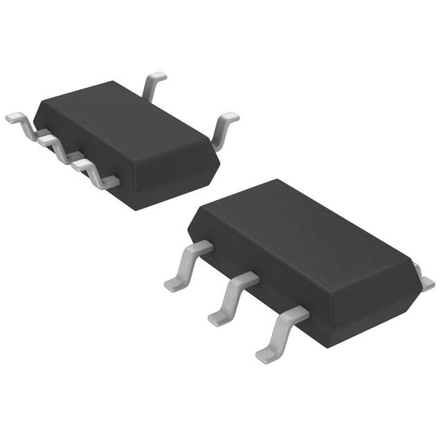
LT3001
36V 4W No-Opto Isolated
Flyback Converter
FEATURES
DESCRIPTION
4V to 36V Input Voltage Range
nn 1.2A, 65V Internal DMOS Power Switch
nn Low Quiescent Current
nn Boundary Mode Operation at Heavy Load
nn Low-Ripple Burst Mode® Operation at Light Load
nn Minimum Load VSW(MAX)
VSW(MAX) = VIN(MAX) + VZENER(MAX)
Example:
VIN(HYS) = 2.5µA • R1
Example:
Choose 2V of hysteresis,
R1 = 806k
Determine the UVLO thresholds and calculate R2
resistor value:
VREVERSE > 53V
A 100V, 0.25A diode from Central Semiconductor
(CMHD4448) is chosen.
VIN(UVLO+) =
1.242V • (R1+R2)
R2
Example:
Set VIN UVLO rising threshold to 7.5V,
Step 6: Select the RFB Resistor.
R2 = 232k
Use the following equation to calculate the starting value
for RFB:
VIN(UVLO+) = 7.5V
R FB =
NPS • (VOUT + VF )
100µA
3 • (5V + 0.3V)
100µA
VIN(UVLO–) = 5.5V
Step 8: Ensure minimum load.
The theoretical minimum load can be approximately estimated as:
Example:
R FB =
+ 2.5µA • R1
= 159k
Depending on the tolerance of standard resistor values,
the precise resistor value may not exist. For 1% standard values, a 158k resistor should be close enough.
The final RFB value should be adjusted on the measured
output voltage.
I LOAD(MIN) =
40µH • (360mA)2 • 10.6kHz
2 • 5V
= 5.5mA
Remember to check the minimum load requirement in
real application. The minimum load occurs at the point
where the output voltage begins to climb up as the converter delivers more energy than what is consumed at
the output. The real minimum load for this application is
about 6mA. In this example, a 820Ω resistor is selected
as the minimum load.
Rev. 0
Information furnished by Analog Devices is believed to be accurate and reliable. However, no responsibility is assumed by Analog
Devices for its use, nor for any infringements of patents or other rights of third parties that may result from its use. Specifications
Forismore
information
www.analog.com
subject to change without notice. No license
granted
by implication
or otherwise under any patent or patent rights of Analog Devices.
9
�LT3001
PACKAGE DESCRIPTION
S5 Package
5-Lead Plastic TSOT-23
(Reference LTC DWG # 05-08-1635 Rev B)
0.62
MAX
0.95
REF
2.90 BSC
(NOTE 4)
1.22 REF
1.4 MIN
3.85 MAX 2.62 REF
2.80 BSC
1.50 – 1.75
(NOTE 4)
PIN ONE
RECOMMENDED SOLDER PAD LAYOUT
PER IPC CALCULATOR
0.30 – 0.45 TYP
5 PLCS (NOTE 3)
0.95 BSC
0.80 – 0.90
0.20 BSC
0.30 – 0.50 REF
0.09 – 0.20
(NOTE 3)
NOTE:
1. DIMENSIONS ARE IN MILLIMETERS
2. DRAWING NOT TO SCALE
3. DIMENSIONS ARE INCLUSIVE OF PLATING
4. DIMENSIONS ARE EXCLUSIVE OF MOLD FLASH AND METAL BURR
5. MOLD FLASH SHALL NOT EXCEED 0.254mm
6. JEDEC PACKAGE REFERENCE IS MO-193
10
0.01 – 0.10
1.00 MAX
DATUM ‘A’
1.90 BSC
S5 TSOT-23 0302 REV B
Rev. 0
08/19
www.analog.com
For more information www.analog.com
ANALOG DEVICES, INC. 2019
�
很抱歉,暂时无法提供与“LT3001ES5#TRPBF”相匹配的价格&库存,您可以联系我们找货
免费人工找货