LT3033
3A, 0.95V to 10V, Very Low Dropout Linear
Regulator with Programmable Current Limit
FEATURES
DESCRIPTION
Single Supply VIN Range: 0.95V to 10V
nn Dropout Voltage: 95mV Typical
nn Output Current: 3A
nn Adjustable Output Voltage: 200mV to 9.7V
nn Single Capacitor Soft-Starts Reference and Lowers
Output Noise
nn Stable with Low ESR, Ceramic Output Capacitors
nn 0.075% Typical Load Regulation from 1mA to 3A
nn Quiescent Current: 1.9mA Typical
nn Quiescent Current in Shutdown: 22μA Typical
nn Power Good (PWRGD) Flag (Status Valid in Shutdown)
nn Current Limit Protection with Foldback
nn Programmable Current Limit
nn Output Current Monitor: I
OUT/2650
nn Thermal Limiting with Hysteresis
nn Reverse Battery, Reverse Output, and Reverse
Current Protection
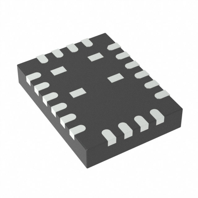
nn 20-Lead 3mm × 4mm QFN Package
The LT®3033 is a very low dropout voltage (VLDO™) linear
regulator that operates from a single input supply down to
0.95V. The device supplies 3A output current with 95mV
typical dropout voltage. The LT3033 is ideal for low input
voltage to low output voltage applications, providing
comparable electrical efficiency to a switching regulator.
nn
APPLICATIONS
The LT3033 optimizes stability and transient response
with low ESR ceramic output capacitors as small as 10μF.
Other features include programmable current limit, an
output current monitor and a power good flag to indicate
output voltage regulation. In shutdown, quiescent current typically drops to 22μA. Internal protection circuitry
includes reverse-battery protection, current limiting with
foldback, thermal limiting with hysteresis and reversecurrent protection.
The LT3033 is available as an adjustable device with an
output voltage down to the 200mV reference. The device
is available in a thermally enhanced, low profile 3mm ×
4mm × 0.75mm QFN package.
All registered trademarks and trademarks are the property of their respective owners.
High Efficiency Linear Regulators
nn Battery-Powered Systems
nn Logic Supplies
nn Post Regulator for Switching Supplies
nn Wireless Modems
nn FPGA Core Supplies
nn
TYPICAL APPLICATION
Minimum Input Voltage vs
Temperature
1.2
1.2V to 0.9V, 3A VLDO Regulator
IN
100k
13.7k
1%
LT3033
SHDN
10µF
IMON
442Ω
GND
10nF
VOUT
0.9V
10µF 3A
ADJ
3.92k
1%
PWRGD
500mV AT
IOUT = 3A
1.1
OUT
ILIM
REF/BYP
10nF
MINIMUM INPUT VOLTAGE (V)
VIN
1.2V
IL = 3A
1.0
0.9
0.8
0.7
0.6
0.5
0.4
0.3
0.2
0.1
0
–75 –50 –25 0 25 50 75 100 125 150 175
TEMPERATURE (°C)
3033 TA01b
3033 TA01a
Rev. A
Document Feedback
For more information www.analog.com
1
�LT3033
ABSOLUTE MAXIMUM RATINGS
PIN CONFIGURATION
(Note 1)
OUT
OUT
OUT
OUT
TOP VIEW
20 19 18 17
IN
21
IN
22
OUT
23
OUT
24
IN 1
IN 2
OUT 3
OUT 4
16 IN
15 IN
14 OUT
13 OUT
12 SHDN
GND 5
11 PWRGD
9 10
ADJ
8
REF/BYP
7
ILIM
GND 6
IMON
IN Pin Voltage..........................................................±10V
OUT Pin Voltage.......................................................±10V
Input-to-Output Differential Voltage.........................±10V
ADJ Pin Voltage.......................................................±10V
REF/BYP Pin Voltage........................................ 1V, –0.3V
SHDN Pin Voltage....................................................±10V
PWRGD Pin Voltage....................................... 10V, –0.3V
ILIM Pin Voltage....................................................... ±7V
IMON Pin Voltage.....................................................±10V
Output Short-Circuit Duration........................... Indefinite
Operating Junction Temperature (Notes 2, 3)
E-/I-grades..........................................–40°C to 125°C
Storage Temperature Range
QFN Package.......................................–65°C to 150°C
UDC PACKAGE
20-LEAD (3mm × 4mm) QFN, IN/OUT EXPOSED PADS
TJMAX = 125°C, θJA = 38°C/W, θJC = 3.4°C/W
ORDER INFORMATION
LEAD FREE FINISH
TAPE AND REEL
PART MARKING*
PACKAGE DESCRIPTION
TEMPERATURE RANGE
LT3033EUDC#PBF
LT3033EUDC#TRPBF
LGVQ
20-Lead (3mm × 4mm) Plastic QFN
–40°C to 125°C
LT3033IUDC#PBF
LT3033IUDC#TRPBF
LGVQ
20-Lead (3mm × 4mm) Plastic QFN
–40°C to 125°C
Contact the factory for parts specified with wider operating temperature ranges. *The temperature grade is identified by a label on the shipping container.
Tape and reel specifications. Some packages are available in 500 unit reels through designated sales channels with #TRMPBF suffix.
2
Rev. A
For more information www.analog.com
�LT3033
ELECTRICAL CHARACTERISTICS
The l denotes the specifications which apply over the full operating
temperature range, otherwise specifications are at TA = 25°C.
PARAMETER
CONDITIONS
MIN
Minimum Input Voltage (Notes 4, 6)
ILOAD = 3A, TA > 0°C
ILOAD = 3A, TA ≤ 0°C
ADJ Pin Voltage (Notes 5, 6, 7)
VIN = 1.5V, ILOAD = 1mA
1.14V < VIN < 10V, 1mA < ILOAD < 3A
l
Line Regulation (Note 13)
VIN = 1.14V to 10V, ILOAD = 1mA
l
Load Regulation (Note 13)
VIN = 1.14V, ILOAD = 1mA to 3A
197
194
TYP
MAX
UNITS
0.95
0.95
1.05
1.14
V
V
200
200
203
206
mV
mV
0.1
1.25
mV
0.15
1
2
mV
mV
45
70
165
mV
mV
55
85
175
mV
mV
70
105
195
mV
mV
95
135
240
mV
mV
1.9
2
3.2
6
13
27
3.5
3.8
7
14
36
60
mA
mA
mA
mA
mA
mA
l
Dropout Voltage
VIN = VOUT(NOMINAL)
(Notes 8, 9)
ILOAD = 100mA
ILOAD = 100mA
l
ILOAD = 500mA
ILOAD = 500mA
l
ILOAD = 1.5A
ILOAD = 1.5A
l
ILOAD = 3A
ILOAD = 3A
l
GND Pin Current
VIN = VOUT(NOMINAL) + 0.4V
(Notes 9, 10)
ILOAD = 0mA
ILOAD = 1mA
ILOAD = 100mA
ILOAD = 500mA
ILOAD = 1.5A
ILOAD = 3A
l
l
l
l
l
l
Output Voltage Noise
COUT = 10μF, ILOAD = 3A, BW = 10Hz to 100kHz,
CREF/BYP = 10nF, VOUT = 1.2V, CFF = 10nF
60
ADJ Pin Bias Current (Notes 9, 11)
VADJ = 0.2V, VIN = 1.5V
5
40
nA
Shutdown Threshold
VOUT = Off to On
VOUT = On to Off
l
l
0.65
0.63
0.95
V
V
SHDN Pin Current (Note 12)
VSHDN = 0V, VIN = 10V
VSHDN = 10V, VIN = 10V
l
l
5.8
±1
15
µA
µA
Quiescent Current in Shutdown
VIN = 6V, VSHDN = 0V
22
37
µA
PWRGD Trip Point
% of Nominal Output Voltage, Output Rising
92
95
%
PWRGD Trip Point Hysteresis
% of Nominal Output Voltage, Output Falling
l
0.25
88
µVRMS
1.9
40
%
PWRGD Output Low Voltage
IPWRGD = 100μA
l
PWRGD Leakage Current
VSHDN = 0V, VPWRGD = 10V
l
150
mV
1
µA
Ripple Rejection (Note 13)
VIN – VOUT = 1V, VRIPPLE = 0.5VP-P,
fRIPPLE = 120Hz, ILOAD = 3A
60
dB
VIN – VOUT = 1V, VRIPPLE = 50mVRMS,
fRIPPLE = 10kHz, ILOAD = 3A
60
dB
VIN – VOUT = 1V, VRIPPLE = 50mVRMS,
fRIPPLE = 1MHz, ILOAD = 3A
52
dB
Internal Current Limit (Note 9)
VIN = 4V, VOUT = 0V
VIN = 1.14V, ∆VOUT = –0.1V
l
l
3.6
3.1
4.5
5.4
A
A
Programmable Current Limit (Note 9)
VIN = 1.5V, RILIM = 332, VOUT = 0V
VIN = 1.5V, RILIM = 162, VOUT = 0V
l
l
1.32
2.64
1.5
3
1.68
3.36
A
A
Input Reverse Leakage Current (Note 14)
VIN = –10V, VOUT = 0V
5
µA
Reverse Output Current (Notes 15, 16)
VOUT = 1.2V, VIN = 0V
0.1
15
µA
Current Monitor Ratio (Note 17)
Ratio = IOUT/IMON
ILOAD = 0.1A, 0.5A, 1.5A, 3A
VIN = 1.5V, VOUT = 1.2V
2650
2650
2782.5
2809
A/A
A/A
TA > 0°C
TA ≤ 0°C
2517.5
2491
Rev. A
For more information www.analog.com
3
�LT3033
ELECTRICAL CHARACTERISTICS
Note 1: Stresses beyond those listed under Absolute Maximum Ratings
may cause permanent damage to the device. Exposure to any Absolute
Maximum Rating condition for extended periods may affect device
reliability and lifetime.
Note 2: The LT3033 is tested and specified under pulse load conditions
such that TJ ≈ TA. The LT3033E is 100% tested at TA = 25°C and
performance is guaranteed from 0°C to 125°C. Performance of the
LT3033E over the full –40°C and 125°C operating junction temperature
range is assured by design, characterization and correlation with statistical
process controls. The LT3033I is guaranteed over the full –40°C to 125°C
operating junction temperature range. High junction temperatures degrade
operating lifetimes. Operating lifetime is derated at junction temperatures
greater than 125°C.
Note 3: The LT3033 includes overtemperature protection that is intended
to protect the device during momentary overload conditions. Junction
temperature exceeds the maximum operating junction temperature when
overtemperature protection is active. Continuous operation above the
specified maximum operating junction temperature may impair device
reliability.
Note 4: Minimum input voltage is the voltage required by the LT3033 to
regulate the output voltage and supply the rated 3A output current. This
specification is tested at VOUT = 0.2V. For higher output voltages, the
minimum input voltage required for regulation equals the regulated output
voltage VOUT plus the dropout voltage or 1.14V, whichever is greater.
Note 5: Maximum junction temperature limits operating conditions. The
regulated output voltage specification does not apply for all possible
combinations of input voltage and output current. Limit the output current
range if operating at maximum input voltage. Limit the input-to-output
voltage differential range if operating at maximum output current.
4
Note 6: The LT3033 typically supplies 3A output current with a 0.95V input
supply. The guaranteed minimum input voltage for 3A output current is
1.14V, especially if cold temperature operation is required.
Note 7: The LT3033 is tested and specified for these conditions with ADJ
tied to OUT.
Note 8: Dropout voltage is the minimum input to output voltage differential
needed to maintain regulation at a specified output current. In dropout the
output voltage equals: (VIN – VDROPOUT).
Note 9: The LT3033 is tested and specified for these conditions with
an external resistor divider (3.92k and 19.6k) setting VOUT to 1.2V. The
external resistor divider adds 50μA of load current.
Note 10: GND pin current is tested with VIN = VOUT(NOMINAL) + 0.4V and a
current source load. GND pin current increases in dropout. See GND pin
current curves in the Typical Performance Characteristics section.
Note 11: Adjust pin bias current flows into the ADJ pin.
Note 12: Shutdown pin current flows into the SHDN pin.
Note 13: The LT3033 is tested and specified for this condition with an
external resistor divider (3.92k and 11.8k) setting VOUT to 0.8V. The
external resistor divider adds 50μA of load current. The specification refers
to the change in the 0.2V reference voltage, not the 0.8V output voltage.
Note 14: Input reverse leakage current flows out of the IN pin.
Note 15: Reverse output current is tested with IN grounded and OUT
forced to the rated output voltage. This current flows into the OUT pin and
out of the GND pin.
Note 16: Reverse current is higher for the case of (rated_output) < VOUT
< VIN, because the no-load recovery circuitry is active in this region and is
trying to restore the output voltage to its nominal value.
Note 17: For detailed information on how to calculate the output current
from the IMON pin, please see the Applications Information section. If the
current monitor function is not needed, the IMON pin must be tied to GND.
Rev. A
For more information www.analog.com
�LT3033
TYPICAL PERFORMANCE CHARACTERISTICS
Dropout Voltage
DROPOUT VOLTAGE (mV)
240
210
TJ = –55°C
TJ = –40°C
TJ = 25°C
TJ = 125°C
TJ = 150°C
180
150
120
90
60
30
0
0
0.5
1
1.5
2
OUTPUT CURRENT (A)
2.5
= TEST POINTS
270
270
240
TJ = 150°C
210
180
150
120
90
TJ = 25°C
60
0
0.5
1
1.5
2
OUTPUT CURRENT (A)
2.5
3033 G01
Minimum Input Voltage
IL = 3A
0.8
0.7
0.6
0.5
0.4
0.3
120
90
60
199
198
197
195
20
10
0
–10
–20
–30
–40
–75 –50 –25 0 25 50 75 100 125 150 175
TEMPERATURE (°C)
194
–75 –50 –25 0 25 50 75 100 125 150 175
TEMPERATURE (°C)
3033 G04
3033 G06
3033 G05
Quiescent Current
Quiescent Current
3.50
Quiescent Current in Shutdown
3.50
100
VSHDN = VIN
VOUT = 1.2V
IL = 0
TJ=25°C
1.40
1.05
0.70
0.35
2.80
2.45
90
QUIESCENT CURRENT (µA)
QUIESCENT CURRENT (mA)
3.15
1.75
2.10
1.75
1.40
1.05
0.70
0.35
0
–75 –50 –25 0 25 50 75 100 125 150 175
TEMPERATURE (°C)
3033 G07
IL = 0.1A
30
200
0.1
2.10
IL = 3A
ADJ Pin Bias Current
201
196
VIN = 1.6V
VSHDN = VIN
VOUT = 1.2V
IL = 0
IL = 0.5A
40
202
0.2
0
–75 –50 –25 0 25 50 75 100 125 150 175
TEMPERATURE (°C)
QUIESCENT CURRENT (mA)
150
IL = 1.5A
3033 G03
ADJ PIN BIAS CURRENT (nA)
203
ADJ PIN VOLTAGE (mV)
MINIMUM INPUT VOLTAGE (V)
0.9
2.45
180
0
–75 –50 –25 0 25 50 75 100 125 150 175
TEMPERATURE (°C)
3
IL = 1mA
205
204
2.80
210
ADJ Pin Voltage
206
1.0
3.15
240
3033 G02
1.2
1.1
VOUT = 1.2V
30
30
0
3
Dropout Voltage
300
DROPOUT VOLTAGE (mV)
VOUT = 1.2V
270
Guaranteed Dropout Voltage
300
GUARANTEED DROPOUT VOLTAGE (mV)
300
TA = 25°C, unless otherwise noted.
0
VIN = 1.6V
VSHDN = 0V
80
70
60
50
40
30
20
10
0
1
2
3 4 5 6 7
INPUT VOLTAGE (V)
8
9
10
3033 G08
0
–75 –50 –25 0 25 50 75 100 125 150 175
TEMPERATURE (°C)
3033 G09
Rev. A
For more information www.analog.com
5
�LT3033
TYPICAL PERFORMANCE CHARACTERISTICS
GND Pin Current
72
VSHDN = 0V
TJ = 25°C
90
GND PIN CURRENT (mA)
60
50
40
30
20
IL = 1mA
IL = 100mA
IL = 500mA
IL = 1.5A
IL = 3A
54
45
36
27
18
1
2
3 4 5 6 7
INPUT VOLTAGE (V)
8
9
10
54
45
IL = 1mA
IL = 100mA
IL = 500mA
IL = 1.5A
IL = 3A
36
27
18
9
0.9
0
1
2
3
4
5
6
INPUT VOLTAGE (V)
7
IL = 1mA
0.5
OFF TO ON
ON TO OFF
0.4
0.3
0.2
10.5
9.0
7.5
6.0
4.5
3.0
1.5
0
0
–75 –50 –25 0 25 50 75 100 125 150 175
TEMPERATURE (°C)
7.5
6.0
4.5
3.0
0
–75 –50 –25 0 25 50 75 100 125 150 175
TEMPERATURE (°C)
3033 G16
0
1
2
3 4 5 6 7 8
SHDN PIN VOLTAGE (V)
10
PWRGD Output Low Voltage
150
95
94
93
92
9
3033 G15
3033 G14
PWRGD TRIP POINT (% OF OUTPUT VOLTAGE)
SHDN PIN INPUT CURRENT (µA)
9.0
1.5
6
12.0
PWRGD Trip Point
10.5
VIN = 10V
13.5
0.6
3
SHDN Pin Input Current
0.7
SHDN Pin Input Current
12.0
0.3 0.6 0.9 1.2 1.5 1.8 2.1 2.4 2.7
OUTPUT CURRENT (A)
3033 G12
0.1
VIN = 10V
VSHDN = 10V
0
15.0
3033 G13
13.5
12
0
8
0.8
0
–75 –50 –25 0 25 50 75 100 125 150 175
TEMPERATURE (°C)
15.0
16
SHDN Pin Threshold
1.0
SHDN PIN THRESHOLD (V)
GND PIN CURRENT (mA)
VIN = 1.6V
VOUT = 1.2V
20
3033 G11
GND Pin Current
63
24
4
SHDN PIN INPUT CURRENT (µA)
0
0
28
8
3033 G10
72
32
9
10
VIN = 1.6V
VOUT = 1.2V
36
PWRGD OUTPUT LOW VOLTAGE (mV)
QUIESCENT CURRENT (µA)
70
0
VOUT = 1.2V
63
80
GND Pin Current
40
GND PIN CURRENT (mA)
Quiescent Current in Shutdown
100
TA = 25°C, unless otherwise noted.
OUTPUT RISING
91
90
OUTPUT FALLING
89
88
–75 –50 –25 0 25 50 75 100 125 150 175
TEMPERATURE (°C)
3033 G17
135
IPWRGD = 100µA
120
105
90
75
60
45
30
15
0
–75 –50 –25 0 25 50 75 100 125 150 175
TEMPERATURE (°C)
3033 G18
Rev. A
For more information www.analog.com
�LT3033
TYPICAL PERFORMANCE CHARACTERISTICS
VPWRGD = 10V
VSHDN = 0V
0.9
Internal Current Limit
0.8
6
0.7
0.6
0.5
0.4
0.3
4
3
VOUT = 0V
VIN = 1.5V
0
1
2
3 4 5 6 7
INPUT VOLTAGE (V)
8
RILIM = 162Ω
2.5
2.0
1.5
RILIM = 332Ω
1.0
0.5
2756.0
2729.5
2703.0
2650.0
2623.5
2597.0
2570.5
2544.0
2491.0
VOUT = 1.2V
VIN = 1.5V
2729.5
2703.0
2676.5
2650.0
2623.5
2597.0
TJ = –55°C
TJ = –40°C
TJ = 25°C
TJ = 125°C
TJ = 150°C
2570.5
2544.0
2517.5
0
0.5
1
1.5
2
OUTPUT CURRENT (A)
0.1 0.2 0.3 0.4 0.5 0.6 0.7 0.8 0.9
VIMON (V)
2729.5
2703.0
2676.5
2650.0
2623.5
2597.0
2570.5
2544.0
1
2491.0
2.5
3
1.8
–15
–20
–25
–30
–35
VIN = –10V
VOUT = 0V
VSHDN = 10V
–50
–75 –50 –25 0 25 50 75 100 125 150 175
TEMPERATURE (°C)
3033 G26
0
0.1 0.2 0.3 0.4 0.5 0.6 0.7 0.8 0.9 1
VIMON (V)
Reverse Output Current
–5
3033 G25
VOUT = 1.2V
VIN = 1.8V
3033 G24
2.0
–45
TJ = –55°C
TJ = –40°C
TJ = 25°C
TJ = 125°C
TJ = 150°C
2756.0
0
–40
IOUT/IMON Current Ratio, IOUT = 3A
2517.5
–10
INPUT CURRENT (µA)
2756.0
0
2809.0
Input Reverse Leakage Current
VOUT = 1.2V
VIN = 1.5V
VIMON = 0.6V
2782.5
3033 G21
3033 G23
IOUT/IMON Current Ratio
VIN = 10V
2.0
2782.5
2676.5
3033 G22
IOUT/IMON CURRENT RATIO (A/A)
TJ = –55°C
TJ = –40°C
TJ = 25°C
TJ = 125°C
TJ = 150°C
2517.5
0
–75 –50 –25 0 25 50 75 100 125 150 175
TEMPERATURE (°C)
2.5
0
–75 –50 –25 0 25 50 75 100 125 150 175
TEMPERATURE (°C)
10
REVERSE OUTPUT CURRENT (mA)
CURRENT LIMIT (A)
3.0
9
IOUT/IMON Current Ratio, IOUT = 3A
2782.5
IOUT/IMON CURRENT RATIO (A/A)
3.5
3.0
0.5
IOUT/IMON CURRENT RATIO (A/A)
2809.0
3.5
1.0
3033 G20
Programmable Current Limit
4.0
1.5
3033 G19
4.0
VIN = 4V
4.5
5
0
0
–75 –50 –25 0 25 50 75 100 125 150 175
TEMPERATURE (°C)
2491.0
5.0
1
0.1
VOUT = 0V
5.5
2
0.2
2809.0
6.0
TJ = –55°C
TJ = –40°C
TJ = 25°C
TJ = 125°C
TJ = 150°C
VOUT = 0V
7
CURRENT LIMIT (A)
PWRGD PIN LEAKAGE CURRENT (µA)
Internal Current Limit
8
CURRENT LIMIT (A)
PWRGD Pin Leakage Current
1.0
TA = 25°C, unless otherwise noted.
1.6
1.4
VIN = 0V
VOUT = 1.2V
IOUT FLOWS INTO OUT PIN
IIN FLOWS OUT OF IN PIN
1.2
1.0
0.8
0.6
0.4
0.2
IOUT
IIN
0
–75 –50 –25 0 25 50 75 100 125 150 175
TEMPERATURE (°C)
3033 G27
Rev. A
For more information www.analog.com
7
�LT3033
TYPICAL PERFORMANCE CHARACTERISTICS
No-Load Recovery Threshold
No-Load Recovery Threshold
25
20
15
10
5
100
14
90
10
IOUT(SINK) = 5mA
8
6
4
IOUT(SINK) = 1mA
10 15 20 25 30 35 40 45 50
OUTPUT OVERSHOOT (%)
3033 G28
RIPPLE REJECTION (dB)
80
70
CREF/BYP = 10nF; C FF =10nF
CREF/BYP = 10nF; CFF = 0
CREF/BYP = 0; CFF = 0
CREF/BYP = 0; CFF = 10nF
60
50
40
30
I
= 3A
20 LOAD
COUT = 10µF
10 VOUT = 1.2V
VIN = 1.5V+50mVRMS RIPPLE
0
10
100
1k
10k 100k
FREQUENCY (Hz)
COUT = 10µF
CREF/BYP = 10nF
CFF = 10nF
VOUT = 1.2V
VIN = 1.5V+50mVRMS RIPPLE
90
80
70
60
50
40
30
ILOAD = 3A
ILOAD = 1.5A
ILOAD = 0.5A
ILOAD = 0.1A
20
10
1M
0
10M
Input Ripple Rejection
80
0.6
LINE REGULATION (mV)
0.8
RIPPLE REJECTION (dB)
90
50
30
20
10
ILOAD = 3A
CREF/BYP = C FF = 10nF
COUT = 10µF
VOUT = 1.2V
VIN = 1.5V+50mV RMS RIPPLE
f = 120Hz
COUT = 10µF
10
10
100
1k
10k 100k
FREQUENCY (Hz)
100
1k
10k 100k
FREQUENCY (Hz)
1M
10M
3033 G30
100
ILOAD = 3A
COUT = 47µF
CREF/BYP = 10nF
CFF = 10nF
VOUT = 1.2V
90
80
70
10kHz
100kHz
500kHz
1MHz
2MHz
60
50
40
30
20
10
1M
0
10M
0
0.1 0.2 0.3 0.4 0.5 0.6 0.7 0.8 0.9
INPUT/OUTPUT DIFFERENTIAL (V)
1
3033 G33
Load Regulation
2.0
∆VIN = 1.14V TO 10V
VOUT = 0.2V
IL = 1mA
1.6
0.4
0.2
0.0
–0.2
–0.4
–0.6
0
–75 –50 –25 0 25 50 75 100 125 150 175
TEMPERATURE (°C)
1.2
0.8
0.4
VIN = 1.14V
VOUT = 0.8V
∆IL = 1mA TO 3A
LOAD REGULATION NUMBER REFERS
TO CHANGE IN THE 200mV REFERENCE
VOLTAGE
0.0
–0.4
–0.8
–1.2
–0.8
–1.6
–1.0
–75 –50 –25 0 25 50 75 100 125 150 175
TEMPERATURE (°C)
–2.0
–75 –50 –25 0 25 50 75 100 125 150 175
TEMPERATURE (°C)
3033 G34
8
0
Line Regulation
1.0
60
COUT = 22µF
3033 G32
100
70
COUT = 47µF
30
Input Ripple Rejection
3033 G31
40
40
Input Ripple Rejection
100
RIPPLE REJECTION (dB)
90
50
3033 G29
Input Ripple Rejection
100
60
10
0
–75 –50 –25 0 25 50 75 100 125 150 175
TEMPERATURE (°C)
RIPPLE REJECTION (dB)
5
70
20
2
0
ILOAD = 3A
CREF/BYP = 10nF
CFF = 10nF
VOUT = 1.2V
VIN = 1.5V+50mV RMS RIPPLE
80
12
LOAD REGULATION (mV)
0
Input Ripple Rejection
16
RIPPLE REJECTION (dB)
TJ = 25°C
OUTPUT OVERSHOOT (%)
OUTPUT SINK CURRENT (mA)
30
TA = 25°C, unless otherwise noted.
3033 G35
3033 G36
Rev. A
For more information www.analog.com
�LT3033
Output Noise Spectral Density
CREF/BYP = 0, CFF = 0
1
0.1
VOUT = 5V
VOUT = 3.3V
VOUT = 2.5V
VOUT = 1.8V
VOUT = 1.5V
VOUT = 1.2V
VOUT = 0.9V
VOUT = 0.2V
0.01
0.001
10
100
1k
10k
FREQUENCY (Hz)
100k
1M
10
1
0.1
0.01
0.001
CFF = 0pF
CFF = 100pF
CFF = 1nF
CFF = 10nF
10
100
3033 G37
360
360
VOUT = 1.5V
VOUT = 1.2V
VOUT = 0.9V
VOUT = 0.2V
180
0
0.01
f = 10Hz TO 100kHz
COUT = 10µF
1
10
100
1k
OUTPUT CURRENT (mA)
1k
10k
FREQUENCY (Hz)
270
240
50
40
30
180
0.1
1
10
100
1k
OUTPUT CURRENT (mA)
120
90 VOUT = 1.5V
VOUT = 1.2V
60
3033 G39
0
10
200
180
VOUT = 0.2V
100
1k
FEEDFORWARD CAPACITOR, CFF (pF)
10k
140
120
100
80
CFF = 10nF
60
20
f = 10Hz TO 100kHz
VOUT = 1.2V
COUT = 10µF
IL = 3A
0
0.01
3033 G41
SHDN Transient Response
CREF/BYP = 0
CFF = 0
160
40
VOUT = 0.9V
10k
RMS Output Noise vs
Bypass Capacitor (CREF/BYP)
VOUT = 1.8V
150
10k
0.1
1
10
100
BYPASS CAPACITOR, CREF/BYP (nF)
1k
3033 G42
SHDN Transient Response
CREF/BYP = 10nF
VOUT
500mV/DIV
VOUT
500mV/DIV
VSHDN
1V/DIV
VSHDN
1V/DIV
2ms/DIV
CREF/BYP = 0pF
CREF/BYP = 100pF
CREF/BYP = 10nF
0
0.01
1M
VOUT = 2.5V
210
3033 G40
VIN = 1.5V
VOUT = 1.2V
RL = 0.4Ω
COUT = 10µF
100k
f = 10Hz TO 100kHz
CREF/BYP = 10nF
COUT = 10µF
IL = 3A
VOUT = 3.3V
30
0.1
60
10
300
240
60
70
20
VOUT = 5V
330
300
120
80
RMS Output Noise vs
Feedforward Capacitor (CFF)
OUTPUT NOISE (µVRMS)
OUTPUT NOISE (µVRMS)
420
VOUT = 5V
VOUT = 3.3V
VOUT = 2.5V
VOUT = 1.8V
f = 10Hz TO 100kHz
90 COUT = 10µF
3033 G38
RMS Output Noise
CREF/BYP = 10nF, CFF = 0
480
100
VOUT = 1.2V
COUT = 10µF
IL = 3A
OUTPUT NOISE (µVRMS)
COUT = 10µF
IL = 3A
RMS Output Noise
VOUT = 0.2V, CFF = 0
OUTPUT NOISE (µVRMS)
10
TA = 25°C, unless otherwise noted.
Output Noise Spectral Density
CREF/BYP = 10nF
OUTPUT NOISE SPECTRAL DENSITY (µV/√Hz)
OUTPUT NOISE SPECTRAL DENSITY (µV/√Hz)
TYPICAL PERFORMANCE CHARACTERISTICS
3033 G43
VIN = 1.5V
VOUT = 1.2V
RL = 0.4Ω
COUT = 10µF
2ms/DIV
3033 G44
Rev. A
For more information www.analog.com
9
�LT3033
TYPICAL PERFORMANCE CHARACTERISTICS
Transient Response
CFF = 0
Start-Up Time
1k
START-UP TIME (ms)
CFF = 10nF
1
0.1
0.01
0.01
10
Transient Response
CFF = 10nF
VOUT = 1.2V
COUT = 10µF
IL = 1mA
100
10
TA = 25°C, unless otherwise noted.
CFF = 0
0.1
1
10
100
BYPASS CAPACITOR, CREF/BYP (nF)
1k
3033 G45
VOUT
100mV/DIV
VOUT
100mV/DIV
IOUT
2A/DIV
IOUT
2A/DIV
100µs/DIV
VIN = 1.5V
VOUT = 1.2V
IOUT = 30mA to 3A
COUT = 47µF
tRISE = tFALL = 100ns
3033 G46
50µs/DIV
VIN = 1.5V
VOUT = 1.2V
IOUT = 30mA to 3A
COUT = 47µF
tRISE = tFALL = 100ns
3033 G47
Rev. A
For more information www.analog.com
�LT3033
PIN FUNCTIONS
IN (Pins 1, 2, 15, 16, Exposed Pad Pins 21, 22): Input.
These pins supply power to the device. The LT3033 requires
a bypass capacitor at IN if located more than six inches from
the main input filter capacitor. Include a bypass capacitor
in battery-powered circuits as a battery’s output impedance rises with frequency. A minimum bypass capacitor
of 10μF suffices. The LT3033 withstands reverse voltages
on the IN pin with respect to ground and the OUT pin. In
the case of a reversed input, which occurs if a battery is
plugged in backwards, the LT3033 behaves as if a diode
is in series with its input. No reverse current flows into
the LT3033 and no reverse voltage appears at the load.
The device protects itself and the load.
OUT (Pins 3, 4, 13, 14, 17, 18, 19, 20, Exposed Pad
Pins 23, 24): Output. These pins supply power to the
load. Use a minimum output capacitor of 10μF to prevent
oscillations. Large load transient applications require larger
output capacitors to limit peak voltage transients. See the
Applications Information section for more information on
output capacitance and reverse-output characteristics.
GND (Pins 5, 6): Ground. Connect the bottom of the external
resistor divider, directly to GND for optimum regulation.
ILIM (Pin 7): Current Limit Programming Pin. This pin is
the collector of a current mirror PNP that is 1/2650th the
size of the output power PNP. This pin is also the input to
the current limit amplifier. Current limit threshold is set by
connecting a resistor between the ILIM pin and GND. For
detailed information on how to set the ILIM pin resistor
value, please see the Applications Information section. If
not used, tie ILIM to ground.
IMON (Pin 8): Output Current Monitor. This pin is the
collector of a PNP current mirror that outputs 1/2650th of
the power PNP current. For detailed information on how
to calculate the output current from the IMON pin, please
see the Applications Information section. If the IMON pin
is not used, tie IMON to GND.
REF/BYP (Pin 9): Reference/Bypass. Connecting a single
capacitor from this pin to GND bypasses the LT3033’s
reference noise and soft-starts the reference. A 10nF bypass capacitor typically reduces output voltage noise to
60μVRMS in a 10Hz to 100kHz bandwidth. Soft-start time
is directly proportional to the REF/BYP capacitor value.
If the LT3033 is placed in shutdown, REF/BYP is actively
pulled low by an internal device to reset soft-start. If low
noise or soft-start performance is not required, this pin
must be left floating (unconnected). Do not drive this pin
with any active circuitry.
ADJ (Pin 10): Adjust. This pin is the error amplifier inverting terminal. Its 5nA typical input bias current flows into
the pin (see curve of ADJ Pin Bias Current vs Temperature
in the Typical Performance Characteristics). The ADJ pin
reference voltage is 200mV (referred to GND).
PWRGD (Pin 11): Power Good. The PWRGD flag is an
open-collector flag to indicate that the output voltage
has increased above 92% of the nominal output voltage.
There is no internal pull-up on this pin; a pull-up resistor
must be used. The PWRGD pin actively pulls low if the
output is less than 90.1% of the nominal output voltage.
The maximum pull-down current of the PWRGD pin in
the low state is 100μA. The PWRGD flag status is valid
in shutdown.
SHDN (Pin 12): Shutdown. Pulling the SHDN pin low
puts the LT3033 into a low power state and turns the
output off. Drive the SHDN pin with either logic or an
open-collector/drain device with a pull-up resistor. The
resistor supplies the pull-up current to the open collector/
drain logic, normally several microamperes, and the SHDN
pin current, typically 5.8μA. If unused, connect the SHDN
pin to VIN. The LT3033 does not function if the SHDN pin
is not connected.
Rev. A
For more information www.analog.com
11
�LT3033
BLOCK DIAGRAM
IN 1, 2, 15, 16, 21, 22
9
12
R3
REF/BYP
THERMAL
SHUTDOWN
SHDN
D1
SHUTDOWN
–
+
200mV
BIAS CURRENT
AND
REFERENCE
GENERATOR
CURRENT
GAIN
Q3
Q2
1/2650
1/2650
Q1
1
Q4
ERROR
AMPLIFIER
3, 4, 13, 14,
17, 18, 19,
20, 23, 24
OUT
IMON
CURRENT
LIMIT
AMPLIFIER
ILIM
–
8
7
+
184mV
D2
210mV
–
NO-LOAD
RECOVERY
Q5
+
R2
10k
11
ADJ
PWRGD
PWRGD
COMPARATOR
Q6
IDEAL
DIODE
+
NOTE:
R1 AND R2 ARE EXTERNAL
10
R1
–
GND 5, 6
12
Rev. A
For more information www.analog.com
�LT3033
APPLICATIONS INFORMATION
The LT3033 very low dropout linear regulator is capable of
0.95V input supply operation. It supplies 3A output current
and dropout voltage is typically 95mV. Quiescent current
is typically 1.9mA and drops to 22μA in shutdown. The
LT3033 incorporates several protection features, making
it ideal for use in battery-powered systems. The device
protects itself against reverse-input and reverse-output
voltages. If the output is held up by a backup battery
when the input is pulled to ground in a battery backup
application, the LT3033 behaves as if a diode is in series
with its output, preventing reverse current flow. In dual
supply applications where the regulator load is returned to
a negative supply, pulling the output below ground by as
much as 10V does not affect start-up or normal operation.
Specifications for output voltages greater than 200mV
are proportional to the ratio of desired output voltage to
200mV (VOUT/200mV). For example, load regulation for
an output current change of 1mA to 3A is typically 150μV
at VADJ = 200mV. At VOUT = 1.5V, load regulation is:
1.5V/200mV • 150μV = 1.125mV
Table 1 shows 1% resistor divider values for some common
output voltages with a resistor divider current equaling or
about 50μA.
Table 1
VOUT (V)
R1 (kΩ)
R2 (kΩ)
0.9
3.92
13.7
1.0
3.92
15.8
Adjustable Operation
1.2
3.92
19.6
The LT3033’s output voltage range
is 0.2V to 9.7V. Figure 1. Adjustable Operation
shows that the external resistor ratio sets output
voltage. The device regulates the output to maintain
ADJ at 200mV referred to ground. If R1's current is
at least 50µA, the ADJ pin bias current can be neglected and R2's current is equal to R1's current. Use
Figure 1’s formula to calculate output voltage. In shutdown,
the output is off and the divider current is zero. Curves of
ADJ Pin Voltage vs Temperature and ADJ Pin Bias Current vs Temperature appear in the Typical Performance
Characteristics section.
1.5
3.92
25.5
1.8
3.92
31.6
2.5
3.92
45.3
3.3
3.92
60.4
5
3.92
95.3
VIN
+
IN
OUT
LT3033
SHDN
VOUT
R2
ADJ
R1
GND
VOUT: 200mV • (1 + R2/R1) + (IADJ • R2)
VADJ: 200mV
IADJ: 5nA AT 25°C
OUTPUT RANGE: 0.2V TO 9.7V
Figure 1. Adjustable Operation
Bypass Capacitance, Output Voltage Noise and
Transient Response
The LT3033 regulator provides low output voltage noise
over the 10Hz to 100kHz bandwidth while operating at
full load with the addition of a reference bypass capacitor
(CREF/BYP) from the REF/BYP pin to GND. A good quality,
low leakage capacitor is recommended. This capacitor
bypasses the internal reference of the regulator, providing a low frequency noise pole. With the use of 10nF for
CREF/BYP, the output voltage noise decreases to as low as
160μVRMS when the output voltage is set for 1.2V. For
higher output voltages (generated by using a feedback
resistor divider), the output voltage noise gains up accordingly when using CREF/BYP by itself.
To lower the output voltage noise for higher output voltages, include a feedforward capacitor (CFF) from VOUT
to the ADJ pin. A good quality, low leakage capacitor is
recommended. This capacitor bypasses the error amplifier
of the regulator, providing a low frequency noise pole. With
the use of 10nF for both CFF and CREF/BYP, output voltage
Rev. A
For more information www.analog.com
13
�LT3033
APPLICATIONS INFORMATION
noise decreases to 60μVRMS when the output voltage is
set to 1.2V by a 50μA feedback resistor divider. If the current in the feedback resistor divider is doubled, CFF must
also be doubled to achieve equivalent noise performance.
Higher values of output voltage noise are often measured
if care is not exercised with regard to circuit layout and
testing. Crosstalk from nearby traces induces unwanted
noise onto the LT3033’s output. Power supply ripple rejection must also be considered. The LT3033 regulator does
not have unlimited power supply rejection and will pass
a small portion of the input noise through to the output.
Using a feedforward capacitor (CFF) from VOUT to the ADJ
pin has the added benefit of improving transient response
for output voltages greater than 0.2V. With no feedforward
capacitor, the settling time will increase as the output voltage is raised above 0.2V (see Transient Response in the
Typical Performance Characteristics section).
During start-up, the internal reference soft-starts if a reference bypass capacitor is present. Regulator start-up time
is directly proportional to the size of the bypass capacitor, slowing to 0.5ms with a 10nF bypass capacitor (See
Start-Up Time in the Typical Performance Characteristics
section). The reference bypass capacitor is actively pulled
low during shutdown to reset the internal reference.
Start-up time is also affected by the use of a feedforward
capacitor. Start-up time is directly proportional to the size
of the feedforward capacitor and output voltage, and is
inversely proportional to the feedback resistor divider current, slowing to 0.4ms with a 10nF feedforward capacitor
and a 10μF output capacitor for an output voltage set to
1.2V by a 50μA feedback resistor divider.
Input Capacitance and Stability
The LT3033 design is stable with a minimum of 10μF
capacitor placed at the IN pin. Very low ESR ceramic
capacitors may be used. However, in cases where long
wires connect the power supply to the LT3033’s input and
ground, use of low value input capacitors combined with
an output load current of greater than 20mA may result
in instability. The resonant LC tank circuit formed by the
14
wire inductance and the input capacitor is the cause and
not a result of LT3033 instability.
The self-inductance, or isolated inductance, of a wire
is directly proportional to its length. However, the wire
diameter has less influence on its self-inductance. For
example, the self-inductance of a 2-AWG isolated wire
with a diameter of 0.26" is about half the inductance of a
30-AWG wire with a diameter of 0.01". One foot of 30-AWG
wire has 465nH of self-inductance.
Several methods exist to reduce a wire’s self-inductance.
One method divides the current flowing towards the
LT3033 between two parallel conductors. In this case,
placing the wires further apart reduces the inductance;
up to a 50% reduction when placed only a few inches
apart. Splitting the wires connects two equal inductors
in parallel. However, when placed in close proximity to
each other, mutual inductance adds to the overall selfinductance of the wires. The most effective technique to
reducing overall inductance is to place the forward and
return current conductors (the input wire and the ground
wire) in close proximity. Two 30-AWG wires separated by
0.02" reduce the overall self-inductance to about one-fifth
of a single wire.
If a battery, mounted in close proximity, powers the LT3033,
a 10μF input capacitor suffices for stability. However, if a
distantly located supply powers the LT3033, use a larger
value input capacitor. Use a rough guideline of 1μF (in
addition to the 10μF minimum) per eight inches of wire
length. The minimum input capacitance needed to stabilize the application also varies with power supply output
impedance variations. Placing additional capacitance on
the LT3033’s output also helps. However, this requires
an order of magnitude more capacitance in comparison
with additional LT3033 input bypassing. Series resistance
between the supply and the LT3033 input also helps stabilize the application; as little as 0.1Ω to 0.5Ω suffices. This
impedance dampens the LC tank circuit at the expense of
dropout voltage. A better alternative is to use higher ESR
tantalum or electrolytic capacitors at the LT3033 input in
place of ceramic capacitors.
Rev. A
For more information www.analog.com
�LT3033
APPLICATIONS INFORMATION
Voltage and temperature coefficients are not the only
sources of problems. Some ceramic capacitors have a
piezoelectric response. A piezoelectric device generates
voltage across its terminals due to mechanical stress,
similar to the way a piezoelectric accelerometer or microphone works. For a ceramic capacitor, the stress
can be induced by vibrations in the system or thermal
transients. The resulting voltages produced can cause appreciable amounts of noise. A ceramic capacitor produced
20
BOTH CAPACITORS ARE 16V,
1210 CASE SIZE, 10µF
0
CHANGE IN VALUE (%)
The LT3033’s design is stable with a wide range of output
capacitors, but is optimized for low ESR ceramic capacitors. The output capacitor’s ESR affects stability, most
notably with small value capacitors. Use a minimum output
capacitor of 10μF with an ESR of less than 0.1Ω to prevent
oscillations. The LT3033 is a low voltage device and output
load transient response is a function of output capacitance.
Larger values of output capacitance decrease the peak
deviations and provide improved transient response for
large load current changes. Ceramic capacitors require extra
consideration. Manufacturers make ceramic capacitors
with a variety of dielectrics; each with a different behavior
across temperature and applied voltage. The most common dielectrics are Z5U, Y5V, X5R and X7R. Z5U and Y5V
dielectrics provide high C-V products in a small package
at low cost, but exhibit strong voltage and temperature
coefficients. X5R and X7R dielectrics yield highly stable
characteristics and are more suitable for use as the output
capacitor at fractionally increased cost. X7R works over a
larger temperature range and exhibits better temperature
stability whereas X5R is less expensive and is available in
higher values. Care still must be exercised when using X5R
and X7R capacitors. The X5R and X7R codes only specify
operating temperature range and maximum capacitance
change over temperature. Capacitance change due to DC
bias with X5R and X7R capacitors is better than Y5V and
Z5U capacitors, but can still be significant enough to drop
capacitor values below appropriate levels. Capacitor DC
bias characteristics tend to improve as component case
size increases, but expected capacitance at operating voltage should be verified. Figure 2 and Figure 3 show voltage coefficient and temperature coefficient comparisons
between Y5V and X5R material.
Figure 4’s trace in response to light tapping from a pencil.
Similar vibration induced behavior can masquerade as
increased output voltage noise.
X5R
–20
–40
–60
Y5V
–80
–100
0
2
4
14
8
6
10 12
DC BIAS VOLTAGE (V)
16
3033 F02
Figure 2. Ceramic Capacitor DC Bias Characteristics
40
20
CHANGE IN VALUE (%)
Output Capacitance and Transient Response
X5R
0
–20
–40
Y5V
–60
–80
BOTH CAPACITORS ARE 16V,
1210 CASE SIZE, 10µF
–100
–50 –25
50
25
75
0
TEMPERATURE (°C)
100
125
3033 F03
Figure 3. Ceramic Capacitor Temperature Characteristics
1mV/DIV
VOUT = 1.3V
COUT = 10µF
ILOAD = 0
1ms/DIV
3033 F04
Figure 4. Noise Resulting from Tapping on a Ceramic Capacitor
Rev. A
For more information www.analog.com
15
�LT3033
APPLICATIONS INFORMATION
No-Load/Light-Load Recovery
A possible transient load step that occurs is where the
output current changes from its maximum level to zero
current or a very small load current. The output voltage
responds by overshooting until the regulator lowers the
amount of current it delivers to the new level. The regulator
loop response time and the amount of output capacitance
control the amount of overshoot. Once the regulator has
decreased its output current, the current provided by the
resistor divider (which sets VOUT) is the only current remaining to discharge the output capacitor from the level
to which it overshot. The amount of time it takes for the
output voltage to recover easily extends to milliseconds
with minimum divider current and many microfarads of
output capacitance.
To eliminate this problem, the LT3033 incorporates a
no-load or light load recovery circuit. This circuit is a
voltage-controlled current sink that significantly improves
the light load transient response time by discharging the
output capacitor quickly and then turning off. The current
sink turns on when the output voltage exceeds 5.3% of
the nominal output voltage. The current sink level is then
proportional to the overdrive above the threshold up to a
maximum of about 27mA. Consult the curve in the Typical
Performance Characteristics for the No-Load Recovery
Threshold.
If external circuitry forces the output above the no-load
recovery circuit’s threshold, the current sink turns on in
an attempt to restore the output voltage to nominal. The
current sink remains on until the external circuitry releases
the output. However, if the external circuitry pulls the
output voltage above the input voltage or the input falls
below the output, the LT3033 turns the current sink off and
shuts down the bias current/reference generator circuitry.
PWRGD Flag
The PWRGD flag indicates that the ADJ pin voltage is
within 8% of the regulated voltage. The PWRGD pin is an
open-collector output, capable of sinking 100μA of current
when the ADJ pin voltage is below 90.1% of the regulated
voltage. There is no internal pull-up on the PWRGD pin;
an external pull-up resistor must be used. As the ADJ
pin voltage rises above 92% of its regulated voltage, the
16
PWRGD pin switches to a high impedance state and the
external pull-up resistor pulls the PWRGD pin voltage up.
During normal operation, an internal glitch filter prevents
the PWRGD pin from switching to a low voltage state if
the ADJ pin voltage falls below the regulated voltage by
more than 10% in a short transient (


 工商网监
湘ICP备2023018690号
工商网监
湘ICP备2023018690号

