LT3479
3A, Full Featured DC/DC
Converter with Soft-Start
and Inrush Current Protection
FEATURES
DESCRIPTION
n
The LT®3479 is a current mode, fixed frequency step-up
DC/DC converter with an internal 3A, 42V switch. Efficiencies of up to 89% can be achieved in typical applications. It
features a programmable soft-start function to limit inductor current during start-up and inrush current protection
to protect the LT3479 during shorts and line transients.
Both inputs of the error amplifier are available to the user
allowing positive and negative output voltages. Through
an external resistor, the user can program the switching frequency from 200kHz to 3.5MHz. The low profile
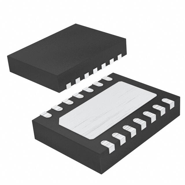
(0.75mm) 14-pin, 4mm × 3mm DFN package provides
excellent thermal performance in a small footprint. The
LT3479 is also available in a thermally enhanced 16-pin
TSSOP package.
n
n
n
n
n
n
n
n
Wide Input Voltage Range: 2.5V to 24V
3A, 42V Internal Switch
High Efficiency Power Conversion: Up to 89%
Soft-Start
Frequency Set by External Resistor: 200kHz to
3.5MHz
Protection Against Input Short Circuits and
Hot Plugging
Low VCESAT Switch: 0.3V at 2.5A (Typical)
Capable of Positive and Negative Outputs
Available in Thermally Enhanced 14-Lead
(4mm × 3mm) DFN and 16-Lead TSSOP Packages
APPLICATIONS
n
n
n
L, LT, LTC, LTM, Linear Technology and the Linear logo are registered trademarks of Linear
Technology Corporation. All other trademarks are the property of their respective owners.
High Power LED Driver
DSL Modems
Distributed Power
TYPICAL APPLICATION
5V to 12V Boost Converter
5V to 12V Efficiency
4.7μH
200k
SW
FBN
SHDN
23.2k
LT3479
VREF
GND
FBP
VC
SS
10nF
RT
85
10μF
EFFICIENCY (%)
2.2μF
VIN VS L
90
VOUT
12V
0.8A
VIN
5V
80
75
70
65
10k
17.8k
2.2nF
3479 TA01
60
0
0.2
0.4
0.6
0.8
IOUT (A)
3479 TA02
3479fc
1
�LT3479
ABSOLUTE MAXIMUM RATINGS
(Note 1)
SW, L, VS Voltages ................................................... 42V
VIN, SHDN Voltages ................................................. 24V
FBP, FBN, VREF, RT, VC Voltages ................................. 2V
Junction Temperature .......................................... 125°C
Operating Temperature Range (Note 2).... –40°C to 85°C
Storage Temperature Range................... –65°C to 125°C
Lead Temperature (Soldering, 10 sec)
TSSOP .............................................................. 300°C
PIN CONFIGURATION
TOP VIEW
TOP VIEW
SW
1
16 GND
SW
1
14 GND
SW
2
15 GND
SW
2
13 GND
L
3
14 GND
L
3
12 SS
VS
4
VS
4
VIN
5
10 FBN
VIN
5
RT
6
9
FBP
RT
6
11 FBN
SHDN
7
8
VREF
SHDN
7
10 FBP
GND
8
9
15
11 VC
DE14 PACKAGE
14-LEAD (4mm s 3mm) PLASTIC DFN
TJMAX = 125°C, θJA = 43°C/W
EXPOSED PAD (PIN 15) IS PGND (MUST BE SOLDERED TO PCB)
17
13 SS
12 VC
VREF
FE PACKAGE
16-LEAD PLASTIC TSSOP
TJMAX = 125°C, θJA = 38°C/W
EXPOSED PAD (PIN 17) IS PGND (MUST BE SOLDERED TO PCB)
ORDER INFORMATION
LEAD FREE FINISH
TAPE AND REEL
PART MARKING
PACKAGE DESCRIPTION
TEMPERATURE RANGE
LT3479EDE#PBF
LT3479EDE#TRPBF
3479
14-Lead (4mm × 3mm) Plastic DFN
–40°C to 85°C
LT3479EFE#PBF
LT3479EFE#TRPBF
3479EFE
16-Lead Plastic TSSOP
–40°C to 85°C
LEAD BASED FINISH
TAPE AND REEL
PART MARKING
PACKAGE DESCRIPTION
TEMPERATURE RANGE
LT3479EDE
LT3479EDE#TR
3479
14-Lead (4mm × 3mm) Plastic DFN
–40°C to 85°C
LT3479EFE
LT3479EFE#TR
3479EFE
16-Lead Plastic TSSOP
–40°C to 85°C
Consult LTC Marketing for parts specified with wider operating temperature ranges.
For more information on lead free part marking, go to: http://www.linear.com/leadfree/
For more information on tape and reel specifications, go to: http://www.linear.com/tapeandreel/
3479fc
2
�LT3479
ELECTRICAL CHARACTERISTICS
The l denotes the specifications which apply over the full operating
temperature range, otherwise specifications are at TA = 25°C. VIN = 2.5V, VSHDN = 2.5V.
PARAMETER
CONDITIONS
MIN
l
Minimum Input Voltage
Quiescent Current
VIN = 2.5V, VSHDN = 0V
VIN = 2.5V, VSHDN = 2.5V, VC = 0.3V (Not Switching)
Reference Voltage
Measured at VREF Pin
Reference Voltage Line Regulation
2.5V < VIN < 24V, VC = 0.3V
Maximum VREF Pin Current
Out of Pin
Soft-Start Pin Current
SS = 0.5V, Out of Pin
l
1.216
TYP
MAX
2.3
2.5
V
0.1
5
1
7.5
μA
mA
1.235
1.250
V
0.01
0.03
%/V
100
μA
9
UNITS
μA
FBP Pin Bias Current
25
100
nA
FBN Pin Bias Current
25
100
nA
2
6
mV
Feedback Amplifier Offset Voltage
FBP – FBN, VC = 1V
–2
Feedback Amplifier Voltage Gain
250
V/V
Feedback Amplifier Transconductance
150
μS
Feedback Amplifier Sink Current
VFBP = 1.25V, VFBN = 1.5V, VC = 0.5V
10
μA
Feedback Amplifier Source Current
VFBP = 1.25V, VFBN = 1V, VC = 0.5V
10
μA
Switching Frequency
RT = 17.8k
RT = 113k
RT = 1.78k
Maximum Switch Duty Cycle
RT = 17.8k
SHDN Pin Current
VSHDN = 5V
VSHDN = 0V
SHDN Pin Threshold
l
0.9
160
2.7
1
200
3.5
84
93
0.3
1.15
240
4.1
MHz
kHz
MHz
%
30
0.1
60
1
μA
μA
1.5
2
V
Inductor Current Limit
(Note 3)
3.5
5
6.5
A
Switch Current Limit
(Note 3)
3
4.5
6
A
Switch VCESAT
ISW = 1A (Note 3)
120
200
mV
Switch Leakage Current
SW = 40V
0.2
5
μA
Note 1: Stresses beyond those listed under Absolute Maximum Ratings
may cause permanent damage to the device. Exposure to any Absolute
Maximum Rating condition for extended periods may affect device
reliability and lifetime.
Note 2: The LT3479 is guaranteed to meet performance specifications
from 0°C to 70°C. Specifications over the –40°C to 85°C operating
temperature range are assured by design, characterization and correlation
with statistical process controls.
Note 3: Inductor Current Limit, Switch Current Limit and Switch VCESAT for
DE package guaranteed by design and/or correlation to static test.
3479fc
3
�LT3479
TYPICAL PERFORMANCE CHARACTERISTICS
Switch VCE(SAT)
Inductor and Switch Current Limit
VREF
6
0.5
1.27
INDUCTOR CURRENT LIMIT
0.3
25°C
–50°C
0.2
0.1
0.5
1
1.5
2
SWITCH CURRENT (A)
2.5
3
1.25
SWITCH CURRENT LIMIT
3
VIN = 24V
1.24
VIN = 2.5V
2
1.23
1
1.22
0
–50 –25
0
0
4
VREF (V)
CURRENT (A)
125°C
VCE(SAT) (V)
1.26
5
0.4
50
25
75
0
TEMPERATURE (°C)
100
1.21
–50 –25
125
SHDN Pin Turn-On Threshold
3479 G03
SHDN Pin Current
VIN Pin Current
50
1.750
6
SHDN THRESHOLD (V)
1.375
30
25°C
20
125°C
10
0
75
0
25
50
TEMPERATURE (°C)
–25
100
125
0
8
4
12
20
Soft-Start Pin Current
3
2
–50 –25
24
Oscillator Frequency
Feedback Amplifier Offset Voltage
RT = 10k
FREQUENCY (MHz)
1.2
RT = 15k
0.8
RT = 20k
4
5
0.4
25 50 75 100 125 150
TEMPERATURE (°C)
3479 G07
25 50 75 100 125 150
TEMPERATURE (°C)
5
1.6
15
10
0
3479 G06
2.0
0
4
3479 G05
20
0
–50 –25
5
VSHDN (V)
3479 G04
ISS (μA)
16
OFFSET VOLTAGE (mV)
1.250
–50
VC = 0.3V
40
VIN PIN CURRENT (mA)
SHDN PIN CURRENT (μA)
–50°C
1.500
25 50 75 100 125 150
TEMPERATURE (°C)
3479 G02
3479 G01
1.625
0
0
–50 –25
VC = 0.5V
3
VC = 1V
2
1
0
25 50 75 100 125 150
TEMPERATURE (°C)
3479 G08
0
–50
–25
0
25
50
TEMPERATURE (oC)
75
100
3479 G09
3479fc
4
�LT3479
PIN FUNCTIONS
(DFN/TSSOP)
SW (Pins 1, 2/Pins 1, 2): Switch Pins. Collector of the
internal NPN power switch. Connect the inductor and diode
here and minimize the metal trace area connected to this
pin to minimize electromagnetic interference.
FBP (Pin 9/Pin 10): The Noninverting Input to the Error
Amplifier. Connect resistive divider tap here for negative
output voltage.
L (Pin 3/Pin 3): Inductor Pin. Connect the inductor to
this pin.
FBN (Pin 10/Pin 11): The Inverting Input to the Error
Amplifier. Connect resistive divider tap here for positive
output voltage.
VS (Pin 4/Pin 4): Inductor Supply. Must be locally bypassed.
Powers the switch and the inductor. In case only one supply
voltage is available, tie VIN and VS together.
VC (Pin 11/Pin 12): Compensation Pin for Error Amplifier.
Connect a series RC from this pin to GND. Typical values
are 10kΩ and 2.2nF.
VIN (Pin 5/Pin 5): Input Supply. Must be locally bypassed.
Powers the internal control circuitry.
SS (Pin 12/Pin 13): Soft-Start. Place a soft-start capacitor
here. Leave floating if not in use.
RT (Pin 6/Pin 6): Timing Resistor Pin. Adjusts the switching frequency. Do not leave this pin open. See Table 4 for
RT values and switching frequencies.
GND (Pins 13, 14/Pins 8, 14, 15, 16): Ground. Tie directly
to local ground plane.
SHDN (Pin 7/Pin 7): Shutdown. Tie to 1.5V or greater to
enable the device. Tie below 0.3V to turn off the device.
Exposed Pad (Pin 15/Pin 17): Power Ground. Must be
connected to electrical PCB ground.
VREF (Pin 8/Pin 9): Bandgap Voltage Reference. Internally
set to 1.235V. Connect this pin to FBP if generating a positive output, or to an external resistor divider if generating a
negative voltage. This pin can provide up to 100μA of current
and can be locally bypassed with a 100pF capacitor.
3479fc
5
�LT3479
BLOCK DIAGRAM
D1
L1
RC
CC
CSS
CS
C1
R1
FB
VS
SS
FBP
+
FEEDBACK
AMPLIFIER
R2
8.5mW
INRUSH CURRENT
PROTECTION
COMPARATOR
+
FBN
SW
L
+
–
36mV
VC
–
–
VREF
SHDN
ICON
MASTER
LATCH
+
pwmout
1.25V
REFERENCE
SLOPE
VIN
CIN
–
PWM
COMPARATOR
R
DRIVER
t
RT
Q1
Q
S
+
3
OSCILLATOR
RT
t
CURRENT LIMIT
COMPARATOR
–
GND
3479 BD
3479fc
6
�LT3479
OPERATION
The LT3479 uses a fixed frequency, current mode control
scheme to provide excellent line and load regulation. Operation can be best understood by referring to the Block
Diagram. The start of each oscillator cycle sets the SR latch
and turns on power switch Q1. The signal at the inverting
input of the PWM comparator (SLOPE) is proportional to
the sum of the switch current and oscillator ramp. When
SLOPE exceeds VC (the output of the feedback amplifier),
the PWM comparator resets the latch and turns off the
power switch. In this manner, the feedback amplifier and
PWM comparators set the correct peak current level to
keep the output in regulation.
The LT3479 also features a soft-start function. During
start-up, 10μA of current charges the external soft-start
capacitor. The SS pin directly limits the rate of voltage rise
on the VC pin, which in turn limits the peak switch current. The switch current is constantly monitored and not
allowed to exceed the nominal value of 3A. If the switch
current reaches 3A, the SR latch is reset regardless of the
output of the PWM comparator. Current limit protects the
power switch and external components.
Soft-start plays an important role in applications where the
switch will reach levels of 30V or higher. During startup,
an overshoot in the switch current together with the presence of high switch voltage can overstress the switch. A
properly used soft-start feature will greatly improve the
robustness of such designs.
In addition to soft-start, inrush current protection protects
the LT3479 against shorts and line transients. During such
faults, the inductor current can momentarily exceed 3A and
damage the switch. Through an internal 8.5mΩ resistor
placed in series with the inductor, the inrush current protection comparator measures the inductor current. If it exceeds
5A, a soft-start cycle is initiated. The LT3479 will remain in
the soft-start condition until the fault has passed.
3479fc
7
�LT3479
APPLICATIONS INFORMATION
Capacitor Selection
Low ESR (equivalent series resistance) ceramic capacitors should be used at the output to minimize the output
ripple voltage. Use only X5R or X7R dielectrics, as these
materials retain their capacitance over wider voltage and
temperature ranges better than other dielectrics. A 4.7μF
to 10μF output capacitor is sufficient for most high output
current designs. Converters with lower output currents
may need only a 1μF or 2.2μF output capacitor.
Table 1. Ceramic Capacitor Manufacturers
MANUFACTURER
PHONE
WEB
Taiyo Yuden
(408) 573-4150
www.t-yuden.com
AVX
(803) 448-9411
www.avxcorp.com
Murata
(714) 852-2001
www.murata.com
Inductor Selection
can pass a current larger than its rated value without
damaging it. Aggressive designs where board space is
precious will exceed the maximum current rating of the
inductor to save board space. Consult each manufacturer
to determine how the maximum inductor current is
measured and how much more current the inductor can
reliably conduct.
Physically larger inductors provide better efficiency than
smaller ones. Figure 1 shows a 3% to 4% efficiency gain
in using a larger inductor in a 1MHz, 5V to 12V application.
The efficiency of the TOKO FDV0630-4R7M, which measures 7mm × 7.7mm and 3 mm thick, peaks at 87%. The
smaller Sumida CDRH4D28-4R7 which is 5mm × 5mm and
3mm thick yields a peak efficiency of 85% in an identical
application. Thus, if board space is abundant, then larger
inductors should be used to maximize efficiency.
90
Several inductors that work well with the LT3479 are listed
in Table 2. However, there are many other manufacturers
and devices that can be used. Consult each manufacturer
for more detailed information and their entire range of
parts. Ferrite core inductors should be used to obtain the
best efficiency. Choose an inductor that can handle the
necessary peak current without saturating, and ensure
that the inductor has a low DCR (copper-wire resistance)
to minimize I2R power losses. A 4.7μH or 10μH inductor
will suffice for most LT3479 applications.
85
EFFICIENCY (%)
80
TOKO FDV0630-4R7
75
SUMIDA CDRH4D28-4R7
70
65
60
55
50
0
0.2
0.4
0.6
0.8
IOUT (A)
Inductor manufacturers specify the maximum current
rating as the current where the inductance falls to some
percentage of its nominal value—typically 65%. An inductor
3479 F01
Figure 1. Efficiency vs Inductor Size
Table 2. Suggested Inductors
MANUFACTURER
PART NUMBER
IDC
(A)
INDUCTANCE
(μH)
MAX DCR
(mΩ)
L×W×H
(mm)
CDRH6D283R0
CDRH6D28100
CDRH4D284R7
3
1.7
1.32
3
10
4.7
24
65
72
6.7 × 6.7 × 3.0
6.7 × 6.7 × 3.0
5.0 × 5.0 × 3.0
Sumida
www.sumida.com
LM N 05D B4R7M
LM N 05D B100K
2.2
1.6
4.7
10
49
10
5.9 × 6.1 × 2.8
5.9 × 6.1 × 2.8
Taiyo Yuden
www.t-yuden.com
LQH55DN4R7M01L
LQH55DN100M01K
2.7
1.7
4.7
10
57
130
5.7 × 5.0 × 4.7
5.7 × 5.0 × 4.7
Murata
www.murata.com
FDV0630-4R7M
4.2
4.7
49
7.0 × 7.7 × 3.0
Toko
www.toko.com
MANUFACTURER
3479fc
8
�LT3479
APPLICATIONS INFORMATION
Diode Selection
Setting Negative Output Voltages
Schottky diodes, with their low forward voltage drop and
fast switching speed, are ideal for LT3479 applications.
Table 3 lists several Schottky diodes that work well with the
LT3479. The diode’s average current rating must exceed
the average output current. The diode’s maximum reverse
voltage must exceed the output voltage. The diode conducts
current only when the power switch is turned off (typically
less than 50% duty cycle), so a 3A diode is sufficient for
most designs. The companies below also offer Schottky
diodes with high voltage and current ratings.
To set a negative output voltage, select the values of R3 and
R4 (see Figure 3) according to the following equation:
⎛ R3 ⎞
VOUT = –1.235V⎜ ⎟
⎝ R4 ⎠
–VOUT
R3
FBP
R4
LT3479
VREF
Table 3. Suggested Diodes
FBN
MANUFACTURER
MAX
MAX REVERSE
PART NUMBER
CURRENT (A) VOLTAGE (V) MANUFACTURER
UPS340
UPS315
3
3
40
15
Microsemi
www.microsemi.com
B220
B230
B240
B320
B330
B340
SBM340
2
2
2
3
3
3
3
20
30
40
20
30
40
40
Diodes, Inc
www.diodes.com
Setting Positive Output Voltages
To set a positive output voltage, select the values of R1 and
R2 (see Figure 2) according to the following equation:
⎛ R1⎞
VOUT = 1.235V⎜ 1 + ⎟
⎝ R2 ⎠
3479 F03
Figure 3. Negative Output Voltage Feedback Connections
Board Layout
As with all switching regulators, careful attention must
be paid to the PCB board layout and component placement. To maximize efficiency, switch rise and fall times
are made as short as possible. To prevent radiation and
high frequency resonance problems, proper layout of the
high frequency switching path is essential. Minimize the
length and area of all traces connected to the SW pin and
always use a ground plane under the switching regulator
to minimize interplane coupling. The signal path including
the switch, output diode D1 and output capacitor COUT,
contains nanosecond rise and fall times and should be
kept as short as possible. Recommended component
placement is shown in Figure 4.
FBP
LT3479
VOUT
VREF
R1
FBN
R2
3479 F02
Figure 2. Positive Output Voltage Feedback Connections
Soft-Start
For many applications, it is necessary to minimize the
inrush current at start-up. The built-in soft-start circuit
significantly reduces the start-up current spike and output
voltage overshoot. A typical value is 10nF for 1.65ms.
Figure 5 shows the start-up output voltage and inductor current waveforms in a typical application without a
soft-start capacitor. Notice the output voltage overshoot
and the large initial current. The addition of a 22nF capacitor eliminates the output overshoot and reduces the peak
inductor current (Figure 6).
3479fc
9
�LT3479
APPLICATIONS INFORMATION
MINIMIZE THE AREA
OF THIS TRACE
TO VOUT
D
COUT
L1
CC
TO VS
SW
GND
SW
GND
CS
CIN
RT
RC
SS
L
VC
LT3479
VS
TO VIN
CSS
VIN
FBN
RT
FBP
R1
VREF
SHDN
R2
TO GND
3479 F04
TO SHDN
PLACE VIAS AROUND EXPOSED PAD
TO ENHANCE THERMAL PERFORMANCE
Figure 4. Suggested Board Layout
Switching Frequency
IL
2A/DIV
The switching frequency of the LT3479 is set by an external resistor attached to the RT pin. Do not leave this pin
open. A resistor must always be connected for proper
operation. See Table 4 and Figure 7 for resistor values
and corresponding frequencies.
VOUT
5V/DIV
0.2MS/DIV
3479 F05
Figure 5. Start-Up with No Soft-Start Capacitor
IL
2A/DIV
VOUT
5V/DIV
0.2ms/DIV
SWITCHING FREQUENCY (MHz)
RT (kΩ)
3.5
1.78
3
2.87
2.5
4.32
2
6.49
1.5
10.2
1
17.8
0.5
39.2
0.2
113
3479 F06
Figure 6. Start-Up with CSS = 22nF
10
Table 4. Switching Frequency
3479fc
�LT3479
APPLICATIONS INFORMATION
Increasing switching frequency reduces output voltage
ripple but also reduces efficiency. The user should set
the frequency for the maximum tolerable output voltage
ripple. Figure 8 shows a reduction in efficiency of about
4% between 1MHz and 2MHz operation in a typical
application.
Inrush Current Protection
The LT3479 features a novel inductor current sensing
circuit that protects the LT3479 during hot plugging and
short circuits. An internal resistor in series with the external inductor senses the inductor current at all times.
When it exceeds 5A, a soft-start cycle is initiated. Figure 9
shows an output overload with inrush current protection
disabled. Notice that soft-start remains high, and that
the inductor current does not return to zero. Figure 10
illustrates the benefits of inrush current protection. The
output short initiates a new soft start cycle reducing the
inductor current. After the fault has passed, the inductor
current slowly returns to its equilibrium value. To ensure
bond wire integrity, the inductor current should not exceed
8A for more than 10ms.
Bypassing the 8.5mΩ inductor current sense resistor
disables inrush current protection. Connect the inductor
supply trace and bypass capacitor to the L pin and leave
the VS pin open to disable this feature.
3.5
VSW
10V/DIV
SWITCH FREQUENCY (MHz)
3.0
2.5
IL
4V/DIV
2.0
VSS
2V/DIV
1.5
VOUT
20V/DIV
1.0
3479 F09
20μs/DIV
0.5
0
0.1
Figure 9. Output Overload with
Inrush Current Protection Enabled
100
10
RT (kΩ)
3479 F07
Figure 7. Switching Frequency
VSW
10V/DIV
IL
4V/DIV
90
1MHz
85
80
EFFICIENCY (%)
VSS
2V/DIV
2MHz
VOUT
20V/DIV
75
3479 F10
70
20μs/DIV
65
Figure 10. Output Overload with
Inrush Current Protection Disabled
60
55
VIN
50
0
0.2
0.4
0.6
0.8
IOUT (A)
VOUT
LT3479
BOOST
REGULATOR
0.5Ω
3479 F08
Figure 8. Efficiency vs Switching Frequency
3479 F11
Figure 11. Circuit for Output Overload
3479fc
11
�LT3479
TYPICAL APPLICATIONS
5V to 12V/800mA 1MHz Boost Converter
90
D1
C1
2.2μF
200k
VIN VS L
SW
FBN
SHDN
C2
10μF
VOUT
12V
0.8A
80
23.2k
LT3479
VREF
SS
RT
GND
85
EFFICIENCY (%)
VIN
5V
L1
4.7μH
Efficiency
FBP
VC
75
70
65
60
55
10nF
10k
17.8k
50
2.2nF
0
0.2
0.4
0.6
C1: TAIYO YUDEN LMK316BJ225MD
C2: AVX 1206 YD106MAT
D1: DIODES INC B320A
L1: TOKO FDV0630-4R7M
3479 TA03b
5V to 12V/800mA 500kHz Boost Converter
L1
10μH
C1
2.2μF
90
D1
200k
VIN VS L
SW
FBN
SHDN
23.2k
LT3479
VREF
SS
RT
GND
Efficiency
FBP
VC
C2
10μF
VOUT
12V
0.8A
85
80
EFFICIENCY (%)
VIN
5V
0.8
IOUT (A)
3479 TA03
75
70
65
60
55
10nF
39.2k
4.7k
50
10nF
3479 TA04
C1: TAIYO YUDEN LMK316BJ225MD
C2: AVX 1206 YD106MAT
D1: DIODES INC. B320A
L1: SUMIDA CDRH8D43-100
0
0.2
0.4
0.6
0.8
IOUT (A)
3479 TA04b
3479fc
12
�LT3479
TYPICAL APPLICATIONS
3.3V to 8V/900mA Boost Converter
90
D1
C1
2.2μF
C2
10μF
169k
VIN VS L
SW
FBN
SHDN
VOU
8V
0.9A
85
80
EFFICIENCY (%)
VIN
3.3V
L1
4.7μH
Efficiency
30.9k
LT3479
VREF
SS
RT
GND
FBP
VC
75
70
65
60
55
4.3k
17.8k
10nF
50
10nF
0
0.2
0.4
0.6
C1: TAIYO YUDEN LMK316BJ225MD
C2: AVX 1206 YD106MAT
D1: DIODES INC B320A
L1: TOKO FDV0630-4R7M
3479 TA03b
5V to –5V/600mA Inverting DC/DC Converter
90
C2
2.2μF
D2
C1
2.2μF
D1
VIN VS L
100k
LT3479
VREF
100pF
SS
RT
10nF
GND
17.8k
C3
10μF
402k
SW
FBP
SHDN
Efficiency
D3
VOUT
–5V
600mA
85
80
EFFICIENCY (%)
VIN
5V
L1
4.7μH
0.8
IOUT (A)
3479 TA05
75
70
65
60
FBN
VC
55
1k
15nF
3479 TA06
C1, C2: TAIYO YUDEN LMK316BJ225MD
C3: AVX 1206 YD106MAT
D1, D2: DIODES INC B320A
D3: CENTRAL SEMI, CMDSH-3-LTC
L1: TOKO FDV0630-4R7M
50
0
0.2
0.4
0.6
0.8
IOUT (A)
3479 TA04b
3479fc
13
�LT3479
TYPICAL APPLICATIONS
500mA, 12 White LED Driver
VIN
2.8V TO 4.2V
L1
4.7μH
D1
C1
2.2μF
D2
600mA
C2
2.2μF
D3
VIN VS L
SW
ON
M1
ON
FBN
SHDN
SS
LT3479
VREF
0.15Ω
124k
FBP
RT
GND
10k
VC
3479 TA07
10nF
7.5k
10k
2.2nF
C1, C2: TAIYO YUDEN LMK316BJ225MD
D1: PHILIPS PMEG 2010
D2, D3: LUMILEDS LXHL-PW01
L1: SUMIDA CDRH4D28-4R7
M1: VISHAY SILICONIX Si2302ADS
3479fc
14
�LT3479
TYPICAL APPLICATIONS
500mA, 12 White LED Driver
L1
10μH
VOUT
16V TO 24V
D1
C1
4.7μF
C2
4.7μF
D2
VIN VS L
SW
100k
FBN
SHDN
LT3479
SS
VREF
93.1k
FBP
RT
5.9k
VC
GND
1Ω
10nF
1Ω
10k
17.8k
ILED
500mA
3.3nF
C1: TAIYO YUDEN EMK316BJ475ML
C2: TAIYO YUDEN TMK325BJ475ML
D1: DIODES INC B330B
D2: LUMILEDS LXHL-NW99
L1: SUMIDA CDRH8D28-100
0.150Ω
3479 TA08
Efficiency
100
VIN = 16V
VIN = 12V
90
EFFICIENCY (%)
VIN
8V TO 16V
VIN = 8V
80
70
60
50
0
0.1
0.2
0.3
IOUT (A)
0.4
0.5
3479 TA08b
3479fc
15
�LT3479
TYPICAL APPLICATIONS
8V, 16V, –8V Triple Output Power Supply for TFTLCD Panels
D2B
VIN
2.8V TO 4.2V
C5
0.1μF
L1
3.3μH
D2A
D1
C3
1μF
16V
10mA
8V
700mA
C1
4.7μF
100k
VIN VS L
SW
FBN
C6
0.1μF
SHDN
LT3479
VREF
GND
FBP
VC
C2
22μF
18.7k
SS
10nF
RT
D3A
–8V
10mA
10k
17.8k
C4
1μF
D3B
2.2nF
D1: MBRM120 OR EQUIVALENT
D2, D3: BAT54S OR EQUIVALENT
L1: SUMIDA CDRH4D28-3R3
C1: AVX 0805ZD475MAT
C2: AVX 1210YD226MAT
C3 TO C6: X5R/X7R 10V
3479 TA10
Efficiency
100
EFFICIENCY (%)
90
80
70
60
50
0
0.1
0.2 0.3 0.4
0.5
LOAD CURRENT (A)
0.6
0.7
3479 TA10b
3479fc
16
�LT3479
TYPICAL APPLICATIONS
1A Dual Tracking Power Supply with Adjustable Outputs
1μF
16V
L1
15μH
VIN
10V TO 14V
4.7μF
16V
D1
VOUT
7V TO 10V
1A
L2
15μH
VIN VS L
30μF
16V
10.2k
SW
470pF
SHDN
FBN
SHDN
LT3479
SS
VCTRL
0V-2.5V
26.1k
VREF
5.76k
1.13k
FBP
RT
VC
GND
10nF
4.99k
10.2k
10k
3.3nF
470pF
1μF
16V
L3
15μH
4.7μF
16V
L4
15μH
30μF
16V
D2
VIN VS L
SW
FBN
SHDN
SS
11.3k
VOUT
–7V TO –10V
1A
LT3479
VREF
FBP
RT
20nF
GND
VC
D3
4.99k
10.2k
3.3nF
3479 TA11
D1, D2: DIODES INC DFLS230 2A, 30V
D3: PHILIPS 1PS79SB62
L1-L4: SUMIDA CDRH6D38-150
ALL CAPACITORS X5R/X7R DIELECTRIC
OR EQUIVALENT
Efficiency
80
VIN =14V, VOUT = p10V
VIN =10V, VOUT = p7V
EFFICIENCY (%)
75
70
VIN = 14V, VOUT = p7V
65
60
55
50
0
0.2
0.4
0.6
IOUT (A)
0.8
1.0
3479 TA11b
3479fc
17
�LT3479
PACKAGE DESCRIPTION
DE Package
14-Lead Plastic DFN (4mm × 3mm)
(Reference LTC DWG # 05-08-1708 Rev B)
0.70 ±0.05
3.30 ±0.05
3.60 ±0.05
2.20 ±0.05
1.70 ± 0.05
PACKAGE
OUTLINE
0.25 ± 0.05
0.50 BSC
3.00 REF
RECOMMENDED SOLDER PAD PITCH AND DIMENSIONS
APPLY SOLDER MASK TO AREAS THAT ARE NOT SOLDERED
R = 0.115
TYP
4.00 ±0.10
(2 SIDES)
R = 0.05
TYP
3.00 ±0.10
(2 SIDES)
8
0.40 ± 0.10
14
3.30 ±0.10
1.70 ± 0.10
PIN 1 NOTCH
R = 0.20 OR
0.35 × 45°
CHAMFER
PIN 1
TOP MARK
(SEE NOTE 6)
(DE14) DFN 0806 REV B
7
0.200 REF
1
0.25 ± 0.05
0.50 BSC
0.75 ±0.05
3.00 REF
0.00 – 0.05
BOTTOM VIEW—EXPOSED PAD
NOTE:
1. DRAWING PROPOSED TO BE MADE VARIATION OF VERSION (WGED-3) IN JEDEC
PACKAGE OUTLINE MO-229
2. DRAWING NOT TO SCALE
3. ALL DIMENSIONS ARE IN MILLIMETERS
4. DIMENSIONS OF EXPOSED PAD ON BOTTOM OF PACKAGE DO NOT INCLUDE
MOLD FLASH. MOLD FLASH, IF PRESENT, SHALL NOT EXCEED 0.15mm ON ANY SIDE
5. EXPOSED PAD SHALL BE SOLDER PLATED
6. SHADED AREA IS ONLY A REFERENCE FOR PIN 1 LOCATION ON THE
TOP AND BOTTOM OF PACKAGE
3479fc
18
�LT3479
PACKAGE DESCRIPTION
FE Package
16-Lead Plastic TSSOP (4.4mm)
(Reference LTC DWG # 05-08-1663)
Exposed Pad Variation BC
4.90 – 5.10*
(.193 – .201)
3.58
(.141)
3.58
(.141)
16 1514 13 12 1110
6.60 p0.10
9
2.94
(.116)
4.50 p0.10
6.40
2.94
(.252)
(.116)
BSC
SEE NOTE 4
0.45 p0.05
1.05 p0.10
0.65 BSC
1 2 3 4 5 6 7 8
RECOMMENDED SOLDER PAD LAYOUT
4.30 – 4.50*
(.169 – .177)
0.09 – 0.20
(.0035 – .0079)
0.50 – 0.75
(.020 – .030)
NOTE:
1. CONTROLLING DIMENSION: MILLIMETERS
MILLIMETERS
2. DIMENSIONS ARE IN
(INCHES)
3. DRAWING NOT TO SCALE
0.25
REF
1.10
(.0433)
MAX
0o – 8o
0.65
(.0256)
BSC
0.195 – 0.30
(.0077 – .0118)
TYP
0.05 – 0.15
(.002 – .006)
FE16 (BC) TSSOP 0204
4. RECOMMENDED MINIMUM PCB METAL SIZE
FOR EXPOSED PAD ATTACHMENT
*DIMENSIONS DO NOT INCLUDE MOLD FLASH. MOLD FLASH
SHALL NOT EXCEED 0.150mm (.006") PER SIDE
3479fc
Information furnished by Linear Technology Corporation is believed to be accurate and reliable.
However, no responsibility is assumed for its use. Linear Technology Corporation makes no representation that the interconnection of its circuits as described herein will not infringe on existing patent rights.
19
�LT3479
TYPICAL APPLICATION
Lumiled Driver for Photo Flash with Output Disconnnect
VIN
3.3V TO 4.2V
L1
4.7μH
D1
C1
2.2μF
VIN VS L
ON
C2
2.2μF
D2
SW
FBN
D3
M1
SHDN
LT3479
VREF
115k
SS
RT
10nF
GND
7.5k
FBP
VC
ON
ILED
500mA/100mA
0.2Ω
2.49k
10k
10k
TORCH MODE
ILED = 100mA
2.2nF
FLASH MODE
ILED = 500mA
3479 TA09
C1, C2: TAIYO YUDEN LMK316BJ225MD
D1: PHILIPS PMEG2010
D2, D3: LUMILEDS LXHL-PW01
L1: SUMIDA CDRH4D28-4R7
M1: VISHAY SILICONIX Si2302ADS
Lumileds Start-Up
Lumileds Torch/Flash Transition
VOUT
1V/DIV
ILED
0.2A/DIV
VOUT
AC-COUPLED
500mV/DIV
INDUCTOR
CURRENT
0.5A/DIV
3479 TA09b
0.2ms/DIV
50μs/DIV
ILED 500mA m100mA m500mA
3479 TA09c
RELATED PARTS
PART NUMBER
DESCRIPTION
COMMENTS
LT1618
Constant Current, Constant Voltage 1.4MHz,
High Efficiency Boost Regulator
VIN: 1.6V to 18V, VOUT(MAX) = 5.5V, IQ = 2.5mA, ISD =