LT3510
Monolithic Dual Tracking
2A Step-Down Switching
Regulator
DESCRIPTION
FEATURES
n
n
n
n
n
n
n
n
n
n
n
n
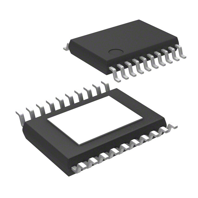
The LT®3510 is a dual current mode PWM step-down
DC/DC converter with two internal 2.5A switches. Independent input voltage, feedback, soft-start and power
good pins for each channel simplify complex power
supply tracking/sequencing requirements.
Wide Input Range: 3.1V to 25V
Two Switching Regulators with 2A Output Capability
Independent Supply to Each Regulator
Adjustable/Synchronizable Fixed Frequency
Operation from 250kHz to 1.5MHz
Antiphase Switching
Outputs Can be Paralleled
Independent, Sequential, Ratiometric or Absolute
Tracking Between Outputs
Independent Soft-Start and Power Good Pins
Enhanced Short-Circuit Protection
Low Dropout: 95% Maximum Duty Cycle
Low Shutdown Current: 10 L ⎜ LIM ⎟
⎝ VOUT ⎠
2
Finally, there must be enough capacitance for good transient
performance. The last equation gives a good starting point.
Alternatively, you can start with one of the designs in this
data sheet and experiment to get the desired performance.
This topic is covered more thoroughly in the section on
loop compensation.
The high performance (low ESR), small size and robustness
of ceramic capacitors make them the preferred type for
LT3510 applications. However, all ceramic capacitors are
not the same. As mentioned above, many of the high value
capacitors use poor dielectrics with high temperature and
voltage coefficients. In particular, Y5V and Z5U types lose
a large fraction of their capacitance with applied voltage
and temperature extremes. Because the loop stability and
transient response depend on the value of COUT, you may
not be able to tolerate this loss. Use X7R and X5R types.
You can also use electrolytic capacitors. The ESRs of most
aluminum electrolytics are too large to deliver low output
ripple. Tantalum and newer, lower ESR organic electrolytic
capacitors intended for power supply use, are suitable
and the manufacturers will specify the ESR. The choice of
capacitor value will be based on the ESR required for low
ripple. Because the volume of the capacitor determines
its ESR, both the size and the value will be larger than a
ceramic capacitor that would give you similar ripple performance. One benefit is that the larger capacitance may
give better transient response for large changes in load
current. Table 2 lists several capacitor vendors.
where ∆IL is the peak-to-peak ripple current in the
inductor.
3510fe
16
�LT3510
APPLICATIONS INFORMATION
Table 2
VENDOR
TYPE
SERIES
Taiyo Yuden
Ceramic X5R, X7R
AVX
Ceramic X5R, X7R
Tantalum
Kemet
Tantalum
TA Organic
AL Organic
T491, T494, T495
T520
A700
Sanyo
TA/AL Organic
POSCAP
Panasonic
AL Organic
SP CAP
TDK
Ceramic X5R, X7R
Catch Diode
The diode D1 conducts current only during switch off
time. Use a Schottky diode to limit forward voltage drop to
increase efficiency. The Schottky diode must have a peak
reverse voltage that is equal to regulator input voltage and
sized for average forward current in normal operation.
Average forward current can be calculated from:
ID(AVG) =
IOUT
• ( VIN – VOUT )
VIN
The only reason to consider a larger diode is the worstcase condition of a high input voltage and shorted output.
With a shorted condition, diode current will increase to a
typical value of 3A, determined by the peak switch current
limit of the LT3510. This is safe for short periods of time,
but it would be prudent to check with the diode manufacturer if continuous operation under these conditions
can be tolerated.
BST Pin Considerations
The capacitor and diode tied to the BST pin generate
a voltage that is higher than the input voltage. In most
cases a 0.47μF capacitor and fast switching diode (such
as the CMDSH-3 or FMMD914) will work well. Almost
any type of film or ceramic capacitor is suitable, but the
ESR should be VIN + 3V
C3
BST
VIN
BST
VIN
SW
LT3510
VIN
SW
LT3510
IND
VOUT
VBST – VSW = VX
VBST(MAX) = VIN + VX
VX(MIN) = 3V
VOUT < 3V
GND
VBST – VSW = VIN
VBST(MAX) = 2 • VIN
(5a)
VIN
SW
VIN
LT3510
IND
VOUT
VOUT < 3V
GND
VBST – VSW = VX
VBST(MAX) = VX
VX(MIN) = VIN + 3V
(5c)
VOUT < 3V
GND
3510 F05
(5d)
Figure 5. BST Pin Considerations
input and output voltages, and on the arrangement of the
boost circuit. The Typical Performance Characteristics
section shows plots of the minimum load current to start
and to run as a function of input voltage for 3.3V and 5V
outputs. In many cases the discharged output capacitor
will present a load to the switcher which will allow it to
start. The plots show the worst-case situation where VIN is
ramping very slowly. Use a Schottky diode for the lowest
start-up voltage.
Frequency Compensation
The LT3510 uses current mode control to regulate the
output. This simplifies loop compensation. In particular, the
LT3510 does not require the ESR of the output capacitor
for stability so you are free to use ceramic capacitors to
achieve low output ripple and small circuit size.
Frequency compensation is provided by the components
tied to the VC pin. Generally a capacitor and a resistor in
series to ground determine loop gain. In addition, there
is a lower value capacitor in parallel. This capacitor is not
part of the loop compensation but is used to filter noise
at the switching frequency.
Loop compensation determines the stability and transient
performance. Designing the compensation network is a bit
complicated and the best values depend on the application
and in particular the type of output capacitor. A practical
approach is to start with one of the circuits in this data
sheet that is similar to your application and tune the compensation network to optimize the performance. Stability
should then be checked across all operating conditions,
including load current, input voltage and temperature.
The LT1375 data sheet contains a more thorough discussion of loop compensation and describes how to test the
stability using a transient load.
Figure 6 shows an equivalent circuit for the LT3510 control
loop. The error amp is a transconductance amplifier with
finite output impedance. The power section, consisting of
the modulator, power switch and inductor, is modeled as
a transconductance amplifier generating an output current proportional to the voltage at the VC pin. Note that
3510fe
18
�LT3510
APPLICATIONS INFORMATION
LT3510
CURRENT MODE
POWER STAGE
gm = 2.2mho
SW
R1
gm = 275μmho
+
–
VC
3.6M
RC
CF
ERROR
AMP
OUTPUT
CPL
ESR
FB
C1
+
CC
0.8V
R2
C1
CERAMIC
TANTALUM
OR
POLYMER
3510 F06
Figure 6. Model for Loop Response
the output capacitor integrates this current, and that the
capacitor on the VC pin (CC) integrates the error amplifier output current, resulting in two poles in the loop. In
most cases a zero is required and comes from either the
output capacitor ESR or from a resistor in series with CC.
This simple model works well as long as the value of the
inductor is not too high and the loop crossover frequency
is much lower than the switching frequency. A phase lead
capacitor (CPL) across the feedback divider may improve
the transient response.
Synchronization
The RT/SYNC pin can be used to synchronize the regulators
to an external clock source. Driving the RT/SYNC resistor
with a clock source triggers the synchronization detection
circuitry. Once synchronization is detected, the rising edge
of SW1 will be synchronized to the rising edge of the
RT/SYNC pin signal. An AGC loop will adjust the internal
oscillators to maintain a 180 degree phase between SW1
and SW2, and also adjust slope compensation to avoid
subharmonic oscillation.
The synchronizing clock signal input to the LT3510 must
have a frequency between 250kHz and 1.5MHz, a duty
cycle between 20% and 80%, a low state below 0.5V and
a high state above 1.6V. Synchronization signals outside
of these parameters will cause erratic switching behavior.
The RT/SYNC resistor should be set such that the free
running frequency ((VRT/SYNC – VSYNCLO)/RRT/SYNC) is
approximately equal to the synchronization frequency. If
the synchronization signal is halted, the synchronization
detection circuitry will timeout in typically 10μs at which
VOUT1
LT3510
PG1
RT/SYNC
VCC
SYNCHRONIZATION
CIRCUITRY
CLK
3510 F07
Figure 7. Synchronous Signal Powered from Regulator’s Output
time the LT3510 reverts to the free-running frequency
based on the current through RT/SYNC. If the RT/SYNC
resistor is held above 2V at any time, switching will be
disabled.
If the synchronization signal is not present during regulator start-up (for example, the synchronization circuitry is
powered from the regulator output) the RT/SYNC pin must
see an equivalent resistance to ground between 15.4k and
133k until the synchronization circuitry is active for proper
start-up operation.
If the synchronization signal powers up in an undetermined
state (VOL, VOH, Hi-Z), connect the synchronization clock
to the LT3510 as shown in Figure 7. The circuit as shown
will isolate the synchronization signal when the output
voltage is below 90% of the regulated output. The LT3510
will start-up with a switching frequency determined by the
resistor from the RT/SYNC pin to ground.
If the synchronization signal powers up in a low impedance
state (VOL), connect a resistor between the RT/SYNC pin
and the synchronizing clock. The equivalent resistance
seen from the RT/SYNC pin to ground will set the start-up
frequency.
3510fe
19
�LT3510
APPLICATIONS INFORMATION
If the synchronization signal powers up in a high impedance
state (Hi-Z), connect a resistor from the RT/SYNC pin to
ground. The equivalent resistance seen from the RT/SYNC
pin to ground will set the start-up frequency.
If the synchronization signal changes between high and
low impedance states during power up (VOL, Hi-Z), connect
the synchronization circuitry to the LT3510 as shown in
the Typical Applications section. This will allow the LT3510
to start-up with a switching frequency determined by the
equivalent resistance from the RT/SYNC pin to ground.
defaults the open-pin condition to be operating (see Typical
Performance Characteristics). Current hysteresis is added
above the SHDN threshold. This can be used to set voltage
hysteresis of the UVLO using the following:
R1=
R2 =
VH – VL
7μA
1.28
VH – 1.28
+ 3μA
R1
Shutdown and Undervoltage Lockout
VH = Turn-on threshold
Figure 8 shows how to add undervoltage lockout (UVLO)
to the LT3510. Typically, UVLO is used in situations where
the input supply is current limited, or has a relatively high
source resistance. A switching regulator draws constant
power from the source, so source current increases as
source voltage drops. This looks like a negative resistance
load to the source and can cause the source to current limit
or latch low under low source voltage conditions. UVLO
prevents the regulator from operating at source voltages
where these problems might occur.
VL = Turn-off threshold
An internal comparator will force the part into shutdown
below the minimum VIN1 of 2.8V. This feature can be
used to prevent excessive discharge of battery-operated
systems.
Since VIN2 supplies the output stage of channel 2 and is
not monitored, care must be taken to insure that VIN2 is
present before channel 2 is allowed to switch.
If an adjustable UVLO threshold is required, the SHDN
pin can be used. The threshold voltage of the SHDN
pin comparator is 1.28V. A 3μA internal current source
LT3510
VIN1
VIN1 > 2.8V
VIN1 OR VIN2
3μA
R1
C1
7μA
+
1.28V
SHDN
R2
–
+
INTERNAL
REGULATOR
Example: switching should not start until the input is above
4.75V and is to stop if the input falls below 3.75V.
VH = 4.75V
VL = 3.75V
R1=
R2 =
4.75 – 3.75
≅ 143k
7μA
1.28
≅ 47k
4.75 – 1.28
+ 3μA
143k
Keep the connections from the resistors to the SHDN
pin short and make sure that the interplane or surface
capacitance to switching nodes is minimized. If high resistor values are used, the SHDN pin should be bypassed
with a 1nF capacitor to prevent coupling problems from
the switch node.
Soft-Start
The output of the LT3510 regulates to the lowest voltage
present at either the SS pin or an internal 0.8V reference.
A capacitor from the SS pin to ground is charged by an
internal 3.25μA current source resulting in a linear output
ramp from 0V to the regulated output whose duration is
given by:
3510 F08
tRAMP =
CSS • 0.8V
3.25μA
Figure 8. Undervoltage Lockout
3510fe
20
�LT3510
APPLICATIONS INFORMATION
At power-up, a reset signal sets the soft-start latch and
discharges both SS pins to approximately 0V to ensure
proper start-up. When both SS pins are fully discharged
the latch is reset and the internal 3.25μA current source
starts to charge the SS pin.
threshold is exceeded. The PG pin is active (sink capability
is reduced in shutdown and undervoltage lockout mode)
as long as the VIN1 pin voltage exceeds 1V.
When the SS pin voltage is below 50mV, the VC pin is pulled
low which disables switching. This allows the SS pin to be
used as an individual shutdown for each channel.
Complex output tracking and sequencing between channels can be implemented using the LT3510’s SS and PG
pins. Figure 9 shows several configurations for output
tracking/sequencing for a 3.3V and 1.8V application.
As the SS pin voltage rises above 50mV, the VC pin is released and the output is regulated to the SS voltage. When
the SS pin voltage exceeds the internal 0.8V reference, the
output is regulated to the reference. The SS pin voltage
will continue to rise until it is clamped at 2V.
Output Tracking/Sequencing
Independent soft-start for each channel is shown in
Figure 9a. The output ramp time for each channel is set
by the soft-start capacitor as described in the soft-start
section.
In the event of a VIN1 undervoltage lockout, the SHDN
pin driven below 1.28V, or the internal die temperature
exceeding its maximum rating during normal operation, the
soft-start latch is set, triggering a start-up sequence.
Ratiometric tracking is achieved in Figure 9b by connecting
both SS pins together. In this configuration, the SS pin
source current is doubled (6.5μA) which must be taken
into account when calculating the output rise time.
In addition, if the load exceeds the maximum output switch
current, the output will start to drop causing the VC pin
clamp to be activated. As long as the VC pin is clamped,
the SS pin will be discharged. As a result, the output will
be regulated to the highest voltage that the maximum
output current can support. For example, if a 6V output
is loaded by 1Ω the SS pin will drop to 0.4V, regulating
the output at 3V ( 3A • 1Ω ). Once the overload condition
is removed, the output will soft-start from the temporary
voltage level to the normal regulation point.
By connecting a feedback network from VOUT1 to the SS2
pin with the same ratio that sets VOUT2 voltage, absolute
tracking shown in Figure 9c is implemented. The minimum
value of the top feedback resistor (R1) should be set such
that the SS pin can be driven all the way to ground with
700μA of sink current when VOUT1 is at its regulated voltage.
In addition, a small VOUT2 voltage offset will be present
due to the SS2 3.25μA source current. This offset can be
corrected for by slightly reducing the value of R2.
Since the SS pin is clamped at 2V and has to discharge
to 0.8V before taking control of regulation, momentary
overload conditions will be tolerated without a soft-start
recovery. The typical time before the SS pin takes control
is:
C • 1.2V
tSS(CONTROL) = SS
700μA
Power Good Indicators
The PG pin is the open-collector output of an internal
comparator. The comparator compares the FB pin voltage
to 90% of the reference voltage with 30mV of hysteresis.
The PG pin has a sink capability of 800μA when the FB pin
is below the threshold and can withstand 25V when the
Figure 9d illustrates output sequencing. When VOUT1 is
within 10% of its regulated voltage, PG1 releases the SS2
soft-start pin allowing VOUT2 to soft-start. In this case PG1
will be pulled up to 2V by the SS pin. If a greater voltage
is needed for PG1 logic, a pull-up resistor to VOUT1 can
be used. This will decrease the soft-start ramp time and
increase tolerance to momentary shorts.
If precise output ramp up and down is required, drive the
SS pins as shown in Figure 9e. The minimum value of
resistor (R3) should be set such that the SS pin can be
driven all the way to ground with 700μA of sink current
during power-up and fault conditions.
Multiple Input Voltages
For applications requiring large inductors due to high VIN
to VOUT ratios, a 2-stage step-down approach may reduce
3510fe
21
�LT3510
APPLICATIONS INFORMATION
Independent Start-Up
Ratiometric Start-Up
Absolute Start-Up
VOUT1
0.5V/DIV
VOUT1
0.5V/DIV
PG1
PG1
PG1
VOUT2
0.5V/DIV
VOUT2
0.5V/DIV
PG2
3.3V
10ms/DIV
3.3V
VOUT1
SS1
0.1μF
LT3510
SS1
0.22μF
LT3510
PG1
VOUT1
1.8V
SS2
3.3V
LT3510
PG1
VOUT2
SS2
PG2
10ms/DIV
VOUT1
SS1
VOUT2
0.5V/DIV
PG2
5ms/DIV
0.1μF
VOUT1
0.5V/DIV
PG1
1.8V
VOUT2
SS2
VOUT2
1.8V
0.22μF
PG2
PG2
PG2
R1
13.7k
R2
8.08k
(9a)
(9b)
Output Sequencing
(9c)
Controlled Power Up and Down
VOUT1
0.5V/DIV
VOUT1
0.5V/DIV
PG1
VOUT2
0.5V/DIV
VOUT2
0.5V/DIV
PG1
SS1/2
PG2
10ms/DIV
10ms/DIV
R3
25k
SS1
0.1μF
VOUT1
3.3V
PG1
SS2
VOUT2
SS1
EXTERNAL
SOURCE
LT3510
1.8V
+
–
LT3510
SS2
3.3V
VOUT1
PG1
1.8V
VOUT2
0.1μF
PG2
PG2
3510 F09
(9d)
(9e)
Figure 9
3510fe
22
�LT3510
APPLICATIONS INFORMATION
VIN
6V TO 24V
4.7μF
PMEG4005
VIN1
3.3μH
0.47μF
PMEG4005
VOUT1
5V
FSET
BST1
BST2
SW1
SW2
B360A
1μH
0.47μF
IND2
VOUT2
42.3k
100k
PG1
FB1
8.06k
470pF
10pF
26.7k
B360A
LT3510
IND1
VOUT1
47μF
VIN2
SHDN
40.2k
47μF
s2
4k
VOUT2
1.2V
PG2
FB2
VC1
VC2
SS/TRACK1 SS/TRACK2
GND
0.1μF
8.06k
470pF
0.1μF
32.4k
10pF
3510 F10
Figure 10. 5V and 1.2V 2-Stage Step-Down Converter with Output Sequencing
inductor size by allowing an increase in frequency. A dual
step down application (Figure 10) steps down the input
voltage (VIN1) to the highest output voltage then uses that
voltage to power the second output (VIN2). VOUT1 must be
able to provide enough current for its output plus VOUT2
maximum load. Note that the VOUT1 must be above VIN2
minimum input voltage (2V) when the second channel
starts to switch. Delaying channel 2 can be accomplished
by either independent soft-start capacitors or sequencing
with the PG1 output.
Single Step Down:
For example, assume a maximum input of 24V:
2-Stage Step-Down:
VIN = 24V, VOUT1 = 5V at 1.5A and VOUT2 = 1.2V at 1.5A
VOUT + VD
V – VSW + VD
Frequency (Hz) ≤ IN
tMIN(ON)
L≥
( VIN – VOUT ) • VOUT
1.2 + 0.6
Frequency (Hz) ≤ 24 – 0.4 + 0.6 = 392kHz
190ns
L1=
L2 =
(24 – 5) • 5
24 • 392kHz
≥ 10μH
(24 – 1.2) • 1.2 ≥ 2.7μH
24 • 392kHz
5 + 0.6
Frequency ≤ 24 – 0.4 + 0.6 = 1.2MHz
190ns
Max Frequency = 1.2MHz
L1=
VIN • f
L2 =
(24 – 5) • 5
24 • 1.2MHz
≥ 3.3μH
(5 – 1.2) • 1.2 ≥ 0.76μH
5 • 1.2MHz
3510fe
23
�LT3510
APPLICATIONS INFORMATION
VIN LT3510 SW
VIN LT3510 SW
VIN LT3510 SW
GND
GND
GND
3510 F11
(11a)
(11b)
(11c)
Figure 11. Subtracting the Current when the Switch is On (11a) from the Current when the Switch is Off (11b) Reveals the Path of the
High Frequency Switching Current (11c). Keep this Loop Small. The Voltage on the SW and BST Traces will Also Be Switched; Keep
These Traces as Short as Possible. Finally, Make Sure the Circuit is Shielded with a Local Ground Plane
PCB Layout
For proper operation and minimum EMI, care must be taken
during printed circuit board (PCB) layout. Figure 11 shows
the high di/dt paths in the buck regulator circuit.
Note that large switched currents flow in the power switch,
the catch diode and the input capacitor. The loop formed
by these components should be as small as possible.
These components, along with the inductor and output
capacitor, should be placed on the same side of the circuit
board and their connections should be made on that layer.
Place a local, unbroken ground plane below these components, and tie this ground plane to system ground at
one location, ideally at the ground terminal of the output
capacitor C2. Additionally, the SW and BST traces should
be kept as short as possible. The topside metal from the
DC964A demonstration board in Figure 12 illustrates proper
component placement and trace routing.
Thermal Considerations
The PCB must also provide heat sinking to keep the LT3510
cool. The exposed metal on the bottom of the package
must be soldered to a ground plane. This ground should
be tied to other copper layers below with thermal vias;
these layers will spread the heat dissipated by the LT3510.
Place additional vias near the catch diodes. Adding more
copper to the top and bottom layers and tying this copper
Figure 12. Topside PCB Layout
3510fe
24
�LT3510
APPLICATIONS INFORMATION
to the internal planes with vias can further reduce thermal resistance. With these steps, the thermal resistance
from die (or junction) to ambient can be reduced to θJA
= 45°C/W.
The power dissipation in the other power components
such as catch diodes, boost diodes and inductors, cause
additional copper heating and can further increase what
the IC sees as ambient temperature. See the LT1767 data
sheet’s Thermal Considerations section.
Single, Low Ripple 4A Output
The LT3510 can generate a single, low ripple 4A output
if the outputs of the two switching regulators are tied
together and share a single output capacitor. By tying the
two FB pins together and the two VC pins together, the
two channels will share the load current. There are several
advantages to this 2-phase buck regulator. Ripple currents
at the input and output are reduced, reducing voltage ripple
and allowing the use of smaller, less expensive capacitors.
Although two inductors are required, each will be smaller
than the inductor required for a single-phase regulator. This
may be important when there are tight height restrictions
on the circuit.
There is one special consideration regarding the 2-phase
circuit. When the difference between the input voltage and
output voltage is less than 2.5V, then the boost circuits may
prevent the two channels from properly sharing current.
If, for example, channel 1 gets started first, it can supply
the load current, while channel 2 never switches enough
current to get its boost capacitor charged.
In this case, channel 1 will supply the load until it reaches
current limit, the output voltage drops, and channel 2 gets
started. Two solutions to this problem are shown in the
Typical Applications section.
The single 3.3V/4A output converter generates a boost supply from either SW that will service both switch pins.
The synchronized 3.3V/8A output converter utilizes
undervoltage lockout to prevent the start-up condition.
Other Linear Technology Publications
Application notes AN19, AN35 and AN44 contain more
detailed descriptions and design information for buck
regulators and other switching regulators. The LT1376
data sheet has a more extensive discussion of output
ripple, loop compensation and stability testing. Design
Note DN100 shows how to generate a dual (+ and –)
output supply using a buck regulator.
3510fe
25
�LT3510
TYPICAL APPLICATIONS
5V and 2.5V with Absolute Tracking
VIN
12V
4.7μF
VIN1
SHDN
3.3μH
0.47μF
BST1
BST2
SW1
SW2
B360A
PMEG4005
VIN2
RT/SYNC
47μF
470pF
8.06k
10pF
PMEG4005
B360A
IND2
VOUT2
100k
42.3k
2.2μH
0.47μF
LT3510
IND1
VOUT1
VOUT1
5V
26.7k
100k
PG1
PG2
FB1
FB2
VC1
VC2
SS/TRACK1 SS/TRACK2
GND
47μF
16.9k
VOUT2
2.5V
470pF
40.2k
40.2k
10pF
8.06k
0.1μF
16.9k
3510 TA02
7.68k
1.25MHz Single 3.3V/4A Low Ripple Output
VIN 6V TO 25V
4.7μF
VIN1
1.5μH
BST1
BST2
SW1
SW2
B360A
24.9k
0.47μF
B360A
LT3510
IND1
VOUT1
47μF
s2
20.5k
RT/SYNC
0.47μF
PMEG4005
VOUT1
3.3V
4A
VIN2
SHDN
1.5μH
PMEG4005
IND2
VOUT2
100k
PG1
FB1
8.06k
1000pF
PG2
FB2
VC1
VC2
SS/TRACK1 SS/TRACK2
GND
22pF
17.8k
0.1μF
3510 TA03
3510fe
26
�LT3510
TYPICAL APPLICATIONS
1.25MHz Single 3.3V/4A Low Ripple Output
VIN 4.5V TO 6V
4.7μF
1μF*
VIN1
VIN2
SHDN
20.5k
RT/SYNC
PMEG4005*
1.5μH
PMEG4005*
BST1
BST2
SW1
SW2
B360A
PMEG4005
B360A
LT3510
47μF
s2
24.9k
PMEG4005
IND2
VOUT2
IND1
VOUT1
VOUT1
3.3V
4A
0.47μF 1.5μH
0.47μF
100k
PG1
FB1
8.06k
1000pF
PG2
FB2
VC1
VC2
SS/TRACK1 SS/TRACK2
GND
22pF
17.8k
0.1μF
3510 TA04
*ADDITIONAL COMPONENTS ADDED TO SHARE THE BOOST VOLTAGE WHEN VIN