LT3762
60V Synchronous Boost
LED Controller
FEATURES
DESCRIPTION
3000:1 External PWM Dimming
nn 250:1 Internal PWM Dimming
nn Wide V Operating Range: 2.5V to 38.5V
IN
nn Synchronous Boost Output Voltage up to 60V
nn Spread-Spectrum Frequency Modulation for Lower EMI
nn PMOS Switch Driver for PWM and Output Disconnect
nn Constant Current (±3.5%) Regulation
nn Constant Voltage (±2%) Regulation
nn Rail-to-Rail LED Current Sense: 0V to 60V
nn Programmable V Undervoltage Lockout
IN
nn Analog Dimming via Two Control Pins
nn 100kHz to 1MHz Operation
nn Programmable Open LED Protection with OPENLED Flag
nn Short-Circuit Protection and SHORTLED Flag
nn Drives LEDs in Boost, SEPIC, Buck Mode, or BuckBoost Mode Configurations
nn 28 Lead TSSOP and QFN (4mm × 5mm) Exposed
Pad Packages
The LT®3762 is a synchronous DC/DC controller designed
to operate as a constant-current source and constantvoltage regulator. It features a programmable internal
PWM dimming signal generator and a synchronous gate
driver. The LT3762 is ideally suited for driving high current LEDs with high efficiency and reduced power loss.
Rail-to-rail switch current sensing enables synchronous
boost topologies and nonsynchronous topologies such
as SEPIC. A voltage feedback pin serves as the input for
several LED protection features and also allows the converter to operate as a constant-voltage source.
nn
A frequency adjust pin allows the user to program the
frequency from 100kHz to 1MHz to optimize efficiency,
performance and external component size. Adding a
capacitor at SSFM pin activates the Spread-Spectrum
Modulation feature to reduce EMI. The LT3762 also includes an integrated DC/DC converter to efficiently produce
a regulated 7.5V supply for the N-channel MOSFET gate
drivers. The PWM pin controls PWMTG to drive the Pchannel MOSFET, allowing a high PWM dimming range
(3000:1) and providing LED overcurrent protection and
short-circuit protected boost capability.
APPLICATIONS
nn
nn
Industrial and Automotive Lighting
Accurate Current-Limited Voltage Regulators
All registered trademarks and trademarks are the property of their respective owners. Protected
by U.S. Patents, including 7199560, 7321203, 7746300. Patents pending.
TYPICAL APPLICATION
98% Efficient 60W Synchronous Boost LED Driver with 3V Minimum Input Voltage
22µH
6mΩ
4.7µF
×3
50V
M2
M1
576k
VIN
SNSP
SNSN
EN/UVLO
INTERNAL PWM DUTY CYCLE
(0.4% TO 100%)
0.1µF
CTRL1
VREF
INTVCC
100k
100k
96
CTRL2
50mΩ
49.9k
82nF
800Hz
3.3nF
5.6k
98
36.5k
BOOST
TG
FB
ISP
LT3762
150k
VDIM = 0V TO 3V
100
SW
348k
66.5k
Efficiency vs Input Voltage
4.7µF
×4
50V
1M
BG
EFFICIENCY (%)
VIN
3V TO 24V
ISN
88
47µH
AUXSW2
OPENLED
SHORTLED
VC
SSFM
6.8nF
AUXSW1
AUXBST
RT
GND
39.2k
200kHz
SS
92
90
M3
PWMTG
DIM
PWM
94
86
0.1µF
10V
30V, 2A LED
CURRENT DERATED
FOR VIN < 8V
0
4
8
12
16
20
INPUT VOLTAGE (V)
24
28
3762 TA01b
INTVCC
0.1µF
10µF
10V
3762 TA01a
Rev 0
Document Feedback
For more information www.analog.com
1
�LT3762
ABSOLUTE MAXIMUM RATINGS
(Note 1)
ISP, ISN......................................................................80V
VIN, EN/UVLO, SNSP, SNSN, SW (Note 7).................60V
CTRL1, CTRL2, OPENLED, SHORTLED.......................15V
FB, PWM, INTVCC, DIM................................................8V
VC, VREF, SS, SSFM......................................................3V
AUXSW1, AUXSW2, TG, BG, PWMTG
BOOST, AUXBST, RT........................................ (Note2)
Operating Junction Temperature Range (Note 3, 4)
LT3762E/LT3762I.................................... –40°C to 125°C
LT3762H................................................. –40°C to 150°C
Storage Temperature Range................... –65°C to 150°C
PIN CONFIGURATION
27 AUXSW2
SHORTLED
3
26 AUXBST
PWM
4
25 AUXSW1
DIM
5
24 VIN
RT
6
23 SNSP
SSFM
7
SS
8
VREF
9
29
GND
AUXBST
2
AUXSW2
OPENLED
TOP VIEW
INTVCC
28 INTVCC
EN/UVLO
1
OPENLED
EN/UVLO
SHORTLED
TOP VIEW
28 27 26 25 24 23
PWM 1
22 AUXSW1
DIM 2
21 VIN
RT 3
22 SNSN
20 SNSP
SSFM 4
21 BG
SS 5
20 BOOST
19 SNSN
29
GND
18 BG
VREF 6
17 BOOST
CTRL1 10
19 SW
CTRL1 7
16 SW
CTRL2 11
18 TG
CTRL2 8
15 TG
VC 12
17 ISP
FB 13
16 ISN
FE PACKAGE
28-LEAD PLASTIC TSSOP
θJA = 30°C/W, θJC = 10°C/W
EXPOSED PAD (PIN 29) IS GND, MUST BE SOLDERED TO PCB
ORDER INFORMATION
LEAD FREE FINISH
TAPE AND REEL
LT3762EFE#PBF
LT3762EFE#TRPBF
LT3762IFE#PBF
LT3762IFE#TRPBF
LT3762HFE#PBF
LT3762HFE#TRPBF
LT3762EUFD#PBF
ISP
ISN
GND
FB
VC
15 PWMTG
PWMTG
GND 14
9 10 11 12 13 14
UFD PACKAGE
28-LEAD (4mm × 5mm) PLASTIC QFN
θJA = 43°C/W, θJC = 3.4°C/W
EXPOSED PAD (PIN 29) IS GND, MUST BE SOLDERED TO PCB
http://www.linear.com/product/LT3762#orderinfo
PART MARKING*
PACKAGE DESCRIPTION
TEMPERATURE RANGE
LT3762
28-Lead Plastic TSSOP
-40°C to 125°C
LT3762
28-Lead Plastic TSSOP
-40°C to 125°C
LT3762
28-Lead Plastic TSSOP
-40°C to 150°C
LT3762EUFD#TRPBF
3762
28-Lead Plastic QFN
-40°C to 125°C
LT3762IUFD#PBF
LT3762IUFD#TRPBF
3762
28-Lead Plastic QFN
-40°C to 125°C
LT3762HUFD#PBF
LT3762HUFD#TRPBF
3762
28-Lead Plastic QFN
-40°C to 150°C
Consult ADI Marketing for parts specified with wider operating temperature ranges. *The temperature grade is identified by a label on the shipping container.
For more information on lead free part marking, go to: http://www.linear.com/leadfree/
For more information on tape and reel specifications, go to: http://www.linear.com/tapeandreel/. Some packages are available in 500 unit reels through
designated sales channels with #TRMPBF suffix.
Rev 0
2
For more information www.analog.com
�LT3762
ELECTRICAL CHARACTERISTICS
The l denotes the specifications which apply over the full operating
temperature range, otherwise specifications are at TA = 25°C. VIN = 24V; CTRL1, CTRL2, PWM = 2V; SW, SSFM = 0V;
INTVCC, BOOST, DIM = 8V unless otherwise noted.
PARAMETER
CONDITIONS
VIN Minimum Operation Voltage
MIN
TYP
VIN Overvoltage Lockout
Rising VIN
Falling Hysteresis
VIN Shutdown IQ
EN/UVLO = 0V
EN/UVLO = 1.15V
VIN Operating IQ (Not Switching)
RT = 82.5k, FB = 1.5V, PWM = 0V
l
INTVCC Operating IQ (Not Switching)
PWM = 0V
VREF Voltage
0µA ≤ IVREF ≤ 250µA
l
VREF Line Regulation
2.5V ≤ VIN ≤ 38.5V
l
Switch Current Sense Limit Threshold
SNSN = 0V, 24V
l
38.5
MAX
V
41
1
43.5
V
V
0.1
1
13
μA
μA
500
µA
3
Current Sense Zero Cross Detect Threshold, VSNSP–SNSN SNSN = 24V, Falling
1.96
UNITS
2.5
l
2
mA
2.04
0.006
V
%/V
72
80
88
mV
3
7
10
mV
Current Sense Zero Cross Detect Threshold Hysteresis
VSNSP-SNSN
SNSN = 24V
2.5
mV
VSNSP, SNSN Synchronous Driver Enable
VSNSP–SNSN > 15mV
SNSP, SNSN Input Bias Current (Low-Side Sensing)
Combined Current Out of Pin, SNSP = SNSN = 0V
22
μA
SNSP, SNSN Input Bias Current (High-Side Sensing)
Combined Current into Pin, SNSP = SNSN = 24V
125
μA
SS Sourcing Current
SS = 0V
28
μA
SS Sinking Current
SS = 2V
2.8
μA
2
V
Error Amplifier
Full-Scale LED Current Sense Threshold (VISP-ISN)
CTRL ≥ 1.2V, ISP = 48V
l
240
249
257
mV
Full-Scale LED Current Sense Threshold (VISP-ISN)
CTRL ≥ 1.2V, ISN = GND (Ground Sensing)
l
232
245
255
mV
1/10th LED Current Sense Threshold (VISP-ISN)
CTRL = 0.2V, ISP = 48V
l
18
22.5
27
mV
1/10th LED Current Sense Threshold (VISP-ISN)
CTRL = 0.2V, ISN = GND (Ground Sensing)
l
10
21
29
mV
½ LED Current Sense Threshold (VISP-ISN)
CTRL = 0.6V, ISP = 48V
l
118
122
126
mV
½ LED Current Sense Threshold (VISP-ISN)
CTRL = 0.6V, ISN = GND (Ground Sensing)
l
110
120
130
ISP/ISN Overcurrent Threshold
ISP = 48V
600
0
ISP/ISN Current Sense Amplifier Input Common Mode
Range (VISN)
ISP/ISN Input Bias Current (Combined)
PWM = 5V (Active), ISP = 48V
PWM = 0V (Standby), ISP = 48V
850
0
ISP/ISN Current Sense Amplifier gm
VISP-ISN = 250mV, ISP = 48V
120
mV
mV
60
V
1
µA
µA
µS
CTRL1,2 Input Bias Current
CTRL = 0V
30
nA
VC Output Impedance
0.9V≤ VC ≤ 1.5V
11
MΩ
VC Standby Input Bias Current
PWM = 0V
–20
FB Regulation Voltage (VFB)
ISP = ISN = 48V, 0V
FB Amplifier gm
FB = VFB, ISP = ISN = 48V
FB Open LED Threshold Rising
OPENLED Falling, ISP Tied to ISN
l
FB Shorted LED Threshold Falling
SHORTLED Falling
l
FB Input Bias Current
FB = 1V
C/10 Inhibit for OPENLED Assertion (VISP-ISN)
ISN = 0V, 48V
l
1.225
20
1.25
1.275
500
VFB–
60mV
V
µS
VFB–
50mV
VFB–
40mV
300
350
mV
39
mV
200
12
nA
25
V
nA
Rev 0
For more information www.analog.com
3
�LT3762
ELECTRICAL CHARACTERISTICS
The l denotes the specifications which apply over the full operating
temperature range, otherwise specifications are at TA = 25°C. VIN = 24V; CTRL1, CTRL2, PWM = 2V; SW, SSFM = 0V;
INTVCC, BOOST, DIM = 8V unless otherwise noted.
PARAMETER
CONDITIONS
FB Overvoltage Threshold Rising
PWMTG rising
l
MIN
TYP
MAX
UNITS
VFB+
55mV
VFB+
65mV
VFB+
75mV
V
VC Current Mode Gain (∆VVC / ∆VSNSP-SNSN)
4
V/V
Oscillator
Switching Frequency (fSWITCH)
RT = 82.5kΩ
RT = 19.6kΩ
RT = 6.65kΩ
Switching Frequency Modulation
VSSFM = 2V
–30
VSSFM = 1V, 2V
12
µA
1
V
BG Minimum On Time
230
ns
BG Minimum Off Time
150
ns
130
ns
VINTVCC
V
l
l
l
90
340
980
105
400
1080
SSFM Input Disable Threshold
SSFM Pin Sink/Source Current
125
460
1240
%fSWITCH
0.95
SSFM Peak-to-Peak Triangle Amplitude
kHz
V
MOSFET Gate Drivers
TG Minimum On Time (Note 5)
BG Drive On Voltage
VINTVCC
–125mV
BG Drive Off Voltage
0.1
TG Drive On Voltage
SW = 0V
TG Drive Off Voltage
SW = 0V
VBOOST
–125mV
VBOOST
V
V
0.1
V
TG, BG Drive Rise Time
CTG = CBG = 2.7nF
20
ns
TG, BG Drive Fall Time
CTG = CBG = 2,7nF
20
ns
PWMTG Driver Output Rise Time
CL = 300pF
50
ns
PWMTG Driver Output Fall Time
CL = 300pF
100
ns
PWMTG On Voltage (VISP – VPWMTG)
PWM = 2V
7
8
V
0
0.3
V
PWMTG Off Voltage (VISP – VPWMTG)
PWM = 0V
BOOST UVLO
VBOOST – VSW
4.2
V
Internal Power Supply
INTVcc Regulation Voltage
INTVcc Undervoltage Lockout Threshold
Falling INTVcc
Rising Hysteresis
INTVcc Line Regulation (∆VINTVCC / ∆VIN)
2.5V < VIN < 38.5V
l
7.3
7.5
7.7
V
l
5.1
5.3
0.4
5.5
V
V
0.002
%/V
Logic Inputs/Outputs
EN/UVLO Threshold Voltage Falling
l
1.185
EN/UVLO Rising Hysteresis
1.220
1.245
6
EN/UVLO Input Low Voltage
IVIN Drops Below 1µA
EN/UVLO Pin Bias Current Low
EN/UVLO = 1.15V
OPENLED Output Low
V
mV
0.4
V
2
2.3
µA
IOPENLED = 500µA
200
300
mV
SHORTLED Output Low
ISHORTLED = 500µA
200
300
mV
OPENLED Pin Bias Current High
OPENLED = 1.30V
10
100
nA
l
1.4
Rev 0
4
For more information www.analog.com
�LT3762
ELECTRICAL CHARACTERISTICS
The l denotes the specifications which apply over the full operating
temperature range, otherwise specifications are at TA = 25°C. VIN = 24V; CTRL1, CTRL2, PWM = 2V; SW, SSFM = 0V;
INTVCC, BOOST, DIM = 8V unless otherwise noted.
PARAMETER
CONDITIONS
TYP
MAX
UNITS
SHORTLED Pin Bias Current High
SHORTLED = 1.30V
10
100
nA
EN/UVLO Pin Bias Current High
EN/UVLO = 1.30V
10
100
nA
V
MIN
PWM Pin Signal Generator
PWM Falling Threshold
DIM = 4V
l
1.25
1.3
1.35
l
0.35
0.43
0.6
PWM Threshold Hysteresis (VPWMHYS)
DIM = 4V
PWM Pull-Up Current (IPWMUP)
DIM = 3.1V, PWM = 0V (100% Duty Cycle)
DIM Input Current
DIM = 5V
PWM Signal Generator Duty Ratio (Note 6)
DIM = 0V
DIM = 1.19V
DIM = 1.42V
DIM = 1.76V
DIM = 2.1V
DIM Input Internal PWM Disable Threshold
RisingDIM
Falling hysteresis
PWM Signal Generator Frequency
PWM = 82nF to GND, DIM = 0.75V, 2.5V
Note 1: Stresses beyond those listed under Absolute Maximum Ratings
may cause permanent damage to the device. Exposure to any Absolute
Maximum Rating condition for extended periods may affect device
reliability and lifetime.
Note 2: Do not apply a positive or negative voltage or current source to
these pins, otherwise, permanent damage may occur.
Note 3: The LT3762E is guaranteed to meet specified performance from
0ºC to 125ºC. Specifications over the –40ºC to 125ºC operating junction
temperature range are assured by design, characterization and correlation
with statistical process controls. The LT3762I is guaranteed to meet
performance specifications over the –40ºC to 125ºC operating junction
temperature range. The LT3762H is guaranteed over the full –40ºC to
150ºC operating junction temperature range. High junction temperatures
degrade operating lifetimes. Operating lifetime is derated at junction
temperatures greater than 125ºC.
5
l
V
µA
1
µA
0.22
3.7
7
17
37
0.32
5
10
25
50
0.4
6.8
13
33
58
%
%
%
%
%
2.9
3.0
25
3.1
V
mV
570
800
1050
Hz
Note 4: The LT3762 includes overtemperature protection that is intended
to protect the device during momentary overload conditions. Junction
temperature will exceed the maximum operating junction temperature
when overtemperature protection is active. Continuous operation above
the specified maximum junction temperature may impair device reliability.
Note 5: Guaranteed by design. A TG pulse will be generated only if the BG
off-time is greater than 310ns (typ). See TG Synchronous Driver under
Duty Cycle Considerations in the Applications Information section.
Note 6: PWM Signal Generator Duty Ratio is calculated by:
Duty = IPWMUP / (IPWMUP + IPWMDN).
Note 7: For operation at Tj < 125°C, the absolute maximum voltage
at VIN, EN/UVLO, SNSP, SNSN, and SW pins is 38.5V for continuous
operation and 60V for up to one second nonrepetitive transients. For
operation at Tj > 125°C, the absolute maximum voltage at VIN, EN/UVLO,
SNSP, SNSN, and SW is 38.5V.
Rev 0
For more information www.analog.com
5
�LT3762
TYPICAL PERFORMANCE CHARACTERISTICS
VISP-ISN Threshold vs CTRL Voltage
TA = 25°C, unless otherwise noted.
VISP-ISN Threshold vs ISP Voltage
300
265
260
150
100
50
VISP–ISN THRESHOLD (mV)
VISP-ISN THRESHOLD (mV)
VISP-ISN THRESHOLD (mV)
200
255
250
245
0.2
0.4
0.6 0.8
VCTRL (V)
1
1.2
240
1.4
126
VISP–ISN THRESHOLD (mV)
INPUT BIAS CURRENT (µA)
245
ISN = 0V
240
500
400
300
200
100
ISN
0
0.0
0.5
20
30
40
ISP VOLTAGE (V)
50
230
–50 –25
60
0
25 50 75 100 125 150
TEMPERATURE (°C)
3762 G03
3762 G02
127
600
FB Regulation Voltage (VFB) vs
Temperature
1.265
ISP = 48V
1.260
125
124
ISP, ISN = 48V
CTRL = 2V
1.255
123
122
121
1.250
1.245
120
119
1.240
118
1
1.5
VCTRL (V)
300
ISP = 48V
250
VISP-ISN Threshold vs
Temperature, CTRL = 0.6V
ISP
700
10
3762 G01
ISP = 48V, PWM = 2V
800
0
VFB (V)
0
ISP/ISN Bias Current vs
CTRL Voltage
900
255
235
0
1000
CTRL = 2V
260
250
–50
VISP-ISN Threshold vs Temperature
117
–50 –25
2
0
3762 G04
1.235
–50 –25
25 50 75 100 125 150
TEMPERATURE (°C)
0
25 50 75 100 125 150
TEMPERATURE (°C)
3762 G05
3762 G06
VREF Source Current vs
Temperature
VISP-ISN Threshold vs FB Voltage
360
2.03
340
2.02
320
2.01
VREF Voltage vs Temperature
VISP-ISN THRESHOLD (mV)
200
150
100
50
0
1.10
1.15
1.2
VFB (V)
1.25
1.3
VREF (V)
VREF MAX SOURCE CURRENT (µA)
CTRL = 2V
250
300
2.00
280
1.99
260
1.98
240
–50 –25
0
25 50 75 100 125 150
TEMPERATURE (°C)
3762 G07
3762 G08
1.97
–50 –25
0
25 50 75 100 125 150
TEMPERATURE (°C)
3762 G09
Rev 0
6
For more information www.analog.com
�LT3762
TYPICAL PERFORMANCE CHARACTERISTICS
Switching Frequency vs
Temperature
Switching Frequency vs RT
1000
500
SNSP–SNSN Current Limit
Threshold vs Temperature
86
RT = 19.6k
900
800
700
600
500
400
300
200
SNSP-SNSN THRESHOLD (mV)
84
SWITCHING FREQUENCY (kHz)
SWITCHING FREQUENCY (kHz)
TA = 25°C, unless otherwise noted.
450
400
350
3
10
300
–50 –25
100
RT (kΩ)
80
78
76
74
70
–50 –25
25 50 75 100 125 150
TEMPERATURE (°C)
SNSP–SNSN Zero Cross
Threshold vs Temperature
86
16
84
84
14
78
76
74
72
82
80
78
76
74
0
0.1
0.2
0.3
SNSN VOLTAGE (V)
0.4
70
0.5
2
10
18
26
SNSN VOLTAGE (V)
34
3762 G13
1.40
2.8
1.35
EN/UVLO THRESHOLD (V)
2.2
2.0
1.8
1.6
1.4
1.0
–50 –25
0
25 50 75 100 125 150
TEMPERATURE (°C)
8
6
4
0
–50 –25
42
0
25 50 75 100 125 150
TEMPERATURE (°C)
3762 G15
INTVCC Maximum Source Current
vs Temperature
150
12VIN, 400kHz fSW
140
1.30
RISING
1.25
1.20
FALLING
1.15
130
120
110
1.10
100
1.05
1.2
10
EN/UVLO Threshold vs
Temperature
3.0
2.4
12
3762 G14
EN/UVLO Hysteresis Current vs
Temperature
2.6
SNSP = 24V
2
72
INTVCC LIMIT (mA)
70
VSNSP–SNSN VOLTAGE (mV)
86
80
25 50 75 100 125 150
TEMPERATURE (°C)
3762 G12
VSNSP–SNSN Current Limit
Threshold vs SNSN Voltage,
SNSN > 2V
82
0
3762 G11
VSNSP-SNSN THRESHOLD (mV)
VSNSP-SNSN THRESHOLD (mV)
0
3762 G10
VSNSP–SNSN Current Limit
Threshold vs SNSN Voltage,
SNSN < 0.5V
HYSTERESIS CURRENT (µA)
82
72
100
0
SNSP = 24V
1.00
–50 –25
0
25 50 75 100 125 150
TEMPERATURE (°C)
3762 G17
3762 G16
90
–50 –25
0
25 50 75 100 125 150
TEMPERATURE (°C)
3762 G18
Rev 0
For more information www.analog.com
7
�LT3762
TYPICAL PERFORMANCE CHARACTERISTICS
VISP-ISN C/10 Threshold vs
Temperature
50
100
850
30
25
20
15
70
60
50
40
30
10
20
5
10
0
25 50 75 100 125 150
TEMPERATURE (°C)
0
0.5
1
1.5
2
2.5
DIM VOLTAGE (V)
3
3762 G19
800
775
40
60
DUTY RATIO (%)
80
250
PWM
500mV/DIV
PWMTG
5V/DIV
LED Current
500mA/DIV
3762 G22
500µs/DIV
100
PWM Pull-Up Current vs
DIM Voltage
CPWM = 82nF, DIM = 1.7V
DIM = INTVCC
PWMTG
5V/DIV
20
3762 G21
PWMTG When PWM Generator
Enabled (Internal PWM Control)
PWM
2V/DIV
0
3762 G20
PWMTG When PWM Generator
Disabled (External PWM Control)
500ns/DIV
825
750
3.5
3762 G23
PWM PULL–UP CURRENT (µA)
0
PWM FREQUENCY (Hz)
PWM DUTY RATIO (%)
80
35
0
–50 –25
CPWM = 82nF
90
40
VISP–ISN VOLTAGE (mV)
PWM Generator Frequency vs
DIM Voltage
PWM Signal Generator Duty Ratio
vs DIM Voltage
ISP = 48V
45
TA = 25°C, unless otherwise noted.
200
150
100
50
0
0
0.5
1
1.5
2
DIM VOLTAGE (V)
2.5
3
3762 G24
4000
4.0
3500
3.8
60
3.6
2500
2000
1500
1000
55
3.4
DUTY CYCLE (%)
3000
3.2
3.0
2.8
2.6
50
45
40
2.4
500
0
PWMTG Duty Ratio vs
Temperature, VDIM = 2V
PWMTG Duty Ratio vs
Temperature, VDIM = 1V
DUTY CYCLE (%)
PWM CURRENT (µA)
PWM Pull-Down Current vs
DIM Voltage
2.2
0
0.5
1
1.5
2
DIM VOLTAGE (V)
2.5
3
2.0
–50 –25
0
25 50 75 100 125 150
TEMPERATURE (°C)
3762 G25
3762 G26
35
–50 –25
0
25 50 75 100 125 150
TEMPERATURE (°C)
3762 G27
Rev 0
8
For more information www.analog.com
�LT3762
TYPICAL PERFORMANCE CHARACTERISTICS
SSFM Current vs Temperature
BG Rise/Fall Time vs Capacitance
80
SINK
11
10
TG Rise/Fall Time vs Capacitance
160
10% TO 90%
70
140
60
120
50
100
TIME (ns)
SOURCE
TIME (ns)
SSFM CURRENT (µA)
13
12
TA = 25°C, unless otherwise noted.
40
30
RISE
20
FALL
0
0
25 50 75 100 125 150
TEMPERATURE (°C)
0
1
2
3 4 5 6 7
CAPACITANCE (nF)
9
INTVCC CURRENT LIMIT IINTVCC_LMT (mA)
INTVCC VOLTAGE (V)
FALL
200
RISE
7.50
12VIN
7.45
2.5VIN
7.40
100
0
1
2
3 4 5 6 7
CAPACITANCE (nF)
8
9
10
0
1
2
3 4 5 6 7
CAPACITANCE (nF)
8
7.35
–50 –25
0
25 50 75 100 125 150
TEMPERATURE (°C)
3762 G32
3762 G31
9
10
3762 G30
200
40VIN
300
0
0
10
7.55
700
TIME (ns)
8
INTVCC vs Temperature, VIN
800
400
RISE
3762 G29
PWMTG Rise/Fall Time vs
Capacitance
500
FALL
60
20
3762 G28
600
80
40
10
9
–50 –25
10% TO 90%
180
INTVCC Maximum Current vs
VIN, fSW
L = 47µH
800kHz 700kHz >900kHz
160
140
600kHz
120
500kHz
100
80
60
400kHz
300kHz
200kHz
40
20
0
100kHz
0 3 6 9 12 15 18 21 24 27 30 33 36 39
VIN (V)
3762 G33
Rev 0
For more information www.analog.com
9
�LT3762
PIN FUNCTIONS
VIN: Power Supply for Internal Loads and INTVCC Regulator. Must be locally bypassed with a 1µF (or larger) low
ESR capacitor placed close to the pin.
EN/UVLO: Shutdown and Undervoltage Detect Pin. An
accurate 1.22V (nominal) falling threshold with externally
programmable hysteresis detects when power is okay to
enable switching. Rising hysteresis is generated by the
external resistor divider and an accurate internal 2μA pulldown current. Tie to 0.4V, or less, to disable the device
and reduce VIN quiescent current below 1μA.
INTVCC: INTVCC is the internal power supply output voltage
node that provides supply for control circuits and NMOS
gate drivers. This pin must be bypassed with a 10µF
ceramic capacitor placed close to the pin.
VC: Transconductance Error Amplifier output pin used
to stabilize the switching regulator control loop with an
RC network. The VC pin is high impedance when PWM is
low. This feature allows the VC pin to store the demand
current state variable for the next PWM high transition.
Connect a capacitor between this pin and GND; a resistor in series with the capacitor is recommended for fast
transient response.
FB: Voltage Loop Feedback Pin. FB is intended for constantvoltage regulation or for LED protection and open LED
detection. The internal transconductance amplifier with
output VC will regulate FB to 1.25V (nominal) through the
DC/DC converter. If the FB input exceeds the regulation
voltage, VFB, minus 50mV (typical) and the voltage between ISP and ISN has dropped below the C/10 threshold
of 25mV (typical), the OPENLED pull-down is asserted.
This action may signal an open LED fault. If FB is driven
above the FB overvoltage threshold, the TG and BG pins
will be driven low and PWMTG driven high to protect the
LEDs from an overcurrent event. If FB 600mV, SHORTLED pull-down is asserted.
Do not leave the FB pin open.
RT: Switching Frequency Adjustment Pin. Set the frequency using a resistor to GND (for resistor values, see
the Typical Performance curve or Table 2). Do not leave
the RT pin open.
SS: Soft-Start Pin. This pin modulates oscillator frequency
and compensation pin voltage (VC) clamp. The soft-start
interval is set with an external capacitor. The pin has a
28μA (typical) pull-up current source to an internal 2.5V
rail. This pin can be used as a fault timer. Provided the
SS pin has exceeded 1.7V, the pull-up current source is
disabled and a 2.8μA pull-down current enabled when
anyone of the following fault conditions happen:
1. LED overcurrent (VISP-ISN > 600mV)
2. INTVCC undervoltage
3. Output short (FB < 0.3V)
4. Thermal limit
The SS pin must be discharged below 0.2V to reinitiate a
soft-start cycle. Switching is disabled until SS begins to
recharge. It is important to select a capacitor large enough
that FB can exceed 0.4V under normal load conditions
before SS exceeds 1.7V. Do not leave this pin open.
BG: The BG pin is the high current gate drive for the lowside N-channel MOSFET.
TG: The TG pin is the high current gate drive for the synchronous N-channel MOSFET.
SW: The SW pin is the high current return path of the
synchronous MOSFET driver and is externally connected
to the negative terminal of the BOOST capacitor. If not
using the synchronous FET, tie this pin to ground.
SNSP: The Positive Current Sense Input for the Switch
Control Loop. Kelvin connect the SNSP pin to the positive
terminal of the switch current sense resistor. Connect to
VIN (after CVIN) for synchronous applications where sense
resistor is in series with the inductor at the supply side.
Connect to the source of low-side FET for nonsynchronous
applications such as SEPIC.
Rev 0
10
For more information www.analog.com
�LT3762
PIN FUNCTIONS
SNSN: The Negative Current Sense Input for the switch
control loop. For synchronous applications, Kelvin connect
the SNSN pin to the negative terminal of the switch current
sense resistor in series with the inductor at the supply
side. For non-synchronous applications such as SEPIC,
Kelvin connect to the ground side of the sense resistor.
ISN: Connection Point for the Negative Terminal of the
Current Feedback Resistor.
ISP: Connection Point for the Positive Terminal of the Current Feedback Resistor. Input bias current depends upon
CTRL pin voltage. When it is greater than INTVCC it flows
into the pin. Below INTVCC, ISP bias current decreases until
it flows out of the pin. If the difference between ISP and
ISN exceeds 600mV (typical), then an overcurrent event
is detected. In response to this event, the BG and TG pins
are driven low and PWMTG is driven high to protect the
switching regulator. Also during an overcurrent event, the
SHORTLED flag is asserted.
PWM: A signal low turns off switcher, idles the oscillator
and disconnects the VC pin from all internal loads.
VPWMTG = VISP – 7V when PWM is above its high threshold,
except in fault conditions. The PWM pin can be driven with
a digital signal to cause pulse width modulation (PWM)
dimming of an LED load. During start-up when SS is below
0.8V, the first rising edge of PWM enables switching which
continues until VISP-ISN ≥ 25mV or SS ≥ 0.8V. Connecting
a capacitor from PWM pin to GND invokes a self-driving
oscillator where internal pull-up and pull-down currents
set a duty ratio at PWMTG pin for dimming LEDs. The
magnitude of the pull-up/down currents is set by the voltage
at the DIM pin and is illustrated in the Typical Performance
Characteristics section. The capacitor on PWM sets the
frequency of the dimming signal. If not used, connect the
PWM and DIM pins to INTVCC.
AUXSW1: The AUXSW1 pin is a switching node of the
auxiliary bias supply. Connect the pin to the auxiliary bias
supply inductor and to the AUXBST pin with a 0.1µF or
larger ceramic capacitor.
AUXSW2: The AUXSW2 node is a switching node of the
INTVCC supply and is connected to the auxiliary bias supply inductor.
AUXBST: The AUXBST pin provides drive voltage to the
INTVCC supply and is connected to the AUXSW1 pin through
a 0.1µF or larger ceramic capacitor.
OPENLED: An open-collector pull-down on this pin asserts
if the FB input is greater than the FB regulation voltage
(VFB) minus 50mV (typical) AND the difference between
current sense inputs ISP and ISN is less than 25mV. The
pin requires an external pull-up resistor, usually to INTVCC.
When the PWM input is low and the DC/DC converter is
idle, the OPENLED condition is latched to the last valid
state when the PWM input was high. When PWM input
goes high again, the OPENLED pin will be updated. This
pin may be used to report transition from constant current regulation to constant voltage regulation modes, for
instance in a charger or current limited voltage supply.
BOOST: The BOOST pin is the supply for the bootstrapped
TG pin gate drive and is externally connected to a low ESR
ceramic BOOST capacitor (0.1µF typ) referenced to the
SW pin. An internal Schottky connects BOOST to INTVCC
for charging this capacitor when SW is pulled to ground
by the bottom FET. If not using a synchronous FET, tie
this pin to INTVCC.
VREF: Reference Output Pin. Can supply up to 250μA. This
pin can drive a resistor divider for the CTRL1, CTRL2 or
DIM pins for dimming or for temperature limit/compensation of LED loads. The normal output voltage is 2V.
CTRL1, CTRL2: Current Sense Threshold Adjustment Pin.
Constant current regulation point VISP-ISN is one-fourth
VCTRL plus an offset for 0V ≤ VCTRL ≤ 1V. For VCTRL > 1.2V
the VISP-ISN current regulation point is constant at the
full-scale value of 250mV. For 1V ≤ VCTRL ≤ 1.2V, the
dependence of VISP-ISN upon CTRL voltage transitions
from a linear function to a constant value, reaching 98% of
full-scale value by VCTRL = 1.1V. Do not leave this pin open.
Exposed Pad and GND: Ground Connection. Solder pin
and exposed pad to ground plane.
Rev 0
For more information www.analog.com
11
�LT3762
PIN FUNCTIONS
SSFM: Used for spread spectrum frequency modulation.
If SSFM is enabled, a triangle ramp is generated at the
SSFM pin. During each cycle of this SSFM ramp, the internal switching frequency is modulated between FSWITCH
and FSWITCH – 30%. The SSFM ramp frequency is set by
12μA/(2 x 1V x CSSFM). If used, tie CSSFM from SSFM to
GND to set the ramp frequency. If not used, tie this pin to
GND. Do not float this pin.
PWMTG: PWM Top-Gate Driver Output. An inverted PWM
signal drives the gate of a series PMOS device between
VISP and (VISP – 7V) if VISP > 7V. An internal 7V clamp
protects the PMOS gate by limiting VGS. Leave PWMTG
disconnected if not used.
SHORTLED: An open-collector pull-down on SHORTLED
asserts when any of the following conditions happen:
This pin requires an external pull-up resistor. SHORTLED
status is only updated during PWM high state and latched
during PWM low state. After an LED overcurrent event,
SHORTLED remains asserted until the SS pin is discharged
below 0.2V.
DIM: Analog voltage control of PWM duty cycle from
0.4% to 97%(typ) when a capacitor is connected between
PWM and ground. When DIM is pulled above 3V (typical),
the PWM duty cycle timer is disabled and the PWM pin
is pulled high with a 5µA current source. The duty cycle
set by VDIM follows a curve shown in Figure 9. A lowpass
RC filter on DIM (10kΩ, 1µF) is recommended if driving
DIM externally to control PWM duty cycle. Do not leave
the DIM pin open. If not used, or if driving PWM externally
connect to INTVCC.
1. FB 600mV).
Rev 0
12
For more information www.analog.com
�LT3762
BLOCK DIAGRAM
PWMTG
VC
ISP
A1
–+
ISP
–+
10µA
PWM _TGOFFB
–
+
+
A2
A10
gm
EAMP
10µA AT
A2+ = A2–
–
TG
PWM
HIGH
SW
SWITCHING
LOGIC
CURRENT
COMPARATOR
X1/4
+
–
1.32V
A11
–
10µA AT
A4+ = A4–
–
ZERO
CROSS DETECT
A5
OVFB
SHORTLED
+
ILIM
A4
+
1.25V
SWITCH
CURRENT SENSE
∑
A6
FAULT
1.2V
FBLOW
300mV
+
SHDN
FBLOW
COMPARATOR
SS AND FAULT
LOGIC
FB
1mA
OVFB
INTVCC
2.8µA
ISP
SCILM
SS
25mV
ISN
SHDN
FAULT
PROTECTION
AND REPORT INTVCC
UVLO
EN/UVLO
IS1
2µA
+
–
A8
SNSP
–
SNSN
A14
OPENLED
+
–
A15
+
VIN
165°C THERMAL
SHUTDOWN
A7
5.3V
INTVCC
AUXSW1
RAMP
GENERATOR
50kHz TO 1MHz
OSCILLATOR
2V
+ –
A9
VVIN
CVIN
AUXBST
RAMP
+
–
1.22V
–+
–
+
A13
PWM_TGOFFB
PWM
HIGH
75mV
A12
3V
OVFB
COMPARATOR
28µA
FB
BG
FAULT
SET
gm
–
INTVCC
A3
FB
BOOST
IPD
+
1.1V
CTRL2
+
+
+
SCILM
–
CTRL1
PWM
TIMER
+
LOAD
CURRENT SENSE
25mV
ISN
INTVCC
+
–
+–
DIM
IPU
SHORT-CIRCUIT
DETECT
–
600mV
PWM
ISP-7V
SET
INTERNAL
POWER
SUPPLY
CAUXBST
LPWR
AUXSW2
INTVCC
GND
CVCC
SSFM
VREF
RT
3762 BD
Rev 0
For more information www.analog.com
13
�LT3762
OPERATION
The LT3762 is a constant-frequency, current mode controller with a low side NMOS gate driver and a high side NMOS
synchronous gate driver. The operation of the LT3762 is
best understood by referring to the Block Diagram. In
this general description, the LT3762 is operating as a
synchronous boost controller where the switch current is
sensed at VIN (sensing at VIN enables TG driver function
for synchronous operation). When power is first applied
to the IC and the PWM pin is low, the BG pin is driven to
GND, the TG pin is driven to SW, and the PWMTG pin is
pulled high to ISP to turn off the PMOS disconnect switch
which disconnects the load from the output of the switching
regulator. The VC pin becomes high impedance to store
the previous switching state on the external compensation capacitor, and the ISP and ISN pin bias currents are
reduced to leakage levels. When the PWM pin transitions
high (either by setting externally or the PWM timer setting
internally), the PWMTG pin transitions low after a short
delay – connecting the load to the output. At the same
time, the internal oscillator wakes up and generates a
pulse to set a latch, turning on the external low side Nchannel MOSFET switch (BG goes high). A voltage input
proportional to the switch current, sensed by an external
current sense resistor between the SNSP and SNSN pins,
is added to a stabilizing slope compensation ramp and
the resulting switch current sense signal is fed into the
negative terminal of the current comparator. The current
in the external inductor increases steadily during the time
the switch is on. When the switch current sense voltage
exceeds the output of the error amplifier, VC, the latch in
logic is reset and the low side switch is turned off. If configured as a synchronous boost controller, once BG goes
low, the zero cross detect comparator determines if the
inductor current is high enough to allow the synchronous
NMOS switch to turn on – preventing the inductor current
from crossing zero and discharging output capacitor. If
the zero cross comparator output is low, TG goes high
(in reference to SW) and turns on the top switch. During
this phase, the inductor current decreases. TG goes low
when either the oscillator terminates the switch cycle or
the inductor current reaches near zero. If configured as a
nonsynchronous boost controller, that is SNSN connected
to GND and the sense resistor placed in the source of the
BG switch, then TG will not switch high during this phase
and a diode placed between SW and the output will conduct
the inductor current until the end of the switch cycle. At the
completion of each oscillator cycle, internal signals such
as slope compensation return to their starting points and
a new cycle begins with the set pulse from the oscillator.
Through this repetitive action, the current mode control
algorithm establishes a switch duty cycle to regulate the
load current or voltage at the load. The VC signal is integrated over many switching cycles and is an amplified
version of the difference between the LED current sense
voltage, measured between ISP and ISN, and the target
difference voltage set by the CTRL pins. In this manner,
the error amplifier sets the correct peak switch current
level to keep the LED current in regulation. If the error
amplifier output increases, more current is demanded in
the switch; if it decreases, less current is demanded. The
switch current is monitored during the on phase and the
voltage between the SNSP and SNSN pins is not allowed
to exceed the current limit threshold of 75mV (typical). If
this current limit is reached, the latch is reset regardless
of the output state of the current comparator and the
TG switch will turn on until the end of the start of a new
switching cycle or the inductor current reaches near zero.
Under fault conditions, i.e. FB overvoltage (FB > 1.3V) ,
output short (FB < 0.3V after start-up), LED overcurrent,
or INTVCC undervoltage (INTVCC < 5.3V), the BG and TG
drivers turn off immediately.
In voltage feedback mode, the operation is similar to that
described above, except the voltage at the VC pin is set by
Rev 0
14
For more information www.analog.com
�LT3762
OPERATION
the amplified difference of the internal reference of 1.25V
and the FB pin. If FB is lower than the reference voltage,
the switch current increases; if FB is higher than the reference voltage, the switch demand current decreases. The
LED current sense feedback interacts with the voltage
feedback so that FB does not exceed the internal reference
and the voltage between ISP and ISN does not exceed
the threshold set by either of the CTRL pins. For accurate
current or voltage regulation, it is necessary to be sure
that under normal operating conditions, the appropriate
loop is dominant. To deactivate the voltage loop entirely,
FB can be set between 0.35V and 1.1V through a resistor
network to VREF pin. To deactivate the LED current loop
entirely, the ISP and ISN pins should be tied together and
CTRL1 and CTRL2 tied to VREF.
Two LED specific functions featured on the LT3762 are
controlled by the voltage feedback FB pin. First, when the
FB pin exceeds a voltage 50mV (–4%) lower than the FB
regulation voltage and V(ISP-ISN) is less than 25mV (typical), the pull-down driver on the OPENLED pin is activated.
This function provides a status indicator that the load may
be disconnected and the constant-voltage feedback loop
is taking control of the switching regulator. When the FB
pin drops below 0.3V after start-up, the SHORTLED pin
is asserted by the FBLOW Comparator. During start-up,
the FBLOW comparator output is blocked from when the
EN/UVLO pin goes high to when the SS pin reaches 1.7V.
The LT3762 features a PMOS disconnect switch driver
that serves two purposes — PWM control of LED load
current and fault protection of LED load. When no fault
condition exists, the PWMTG state depends on the state
of the PWM pin. When PWM pin is high, the PWMTG
is pulled below ISP to turn on the PMOS switch. When
PWM pin is low, PWMTG is pulled to ISP to turn off the
PMOS. Once a fault condition is detected, the PWMTG pin
is pulled high to turn off the PMOS switch — independent
of the PWM pin state. This action isolates the LED array
from the power path, preventing excessive current from
damaging the LEDs.
PWM control of LED load current is achieved by externally
setting the PWM pin or by allowing the internal PWM Timer
to set the PWM pin. If externally controlling the PWM pin,
the DIM pin is set above 3V (e.g. tie to INTVCC). If the
internal PWM Timer is used, PWM pin is connected to an
external capacitor (size of cap sets PWM frequency) and
the voltage at DIM determines the duty cycle at PWMTG.
The duty cycle range is 0.32% to 97% (typical). Setting
DIM above 3V (typ) disables the timer and sets PWM to
100% duty cycle. The relationship between VDIM and the
generated duty cycle allows a linear change in VDIM to be
perceived by the human eye as a linear change in LED
intensity.
The INTVCC rail is generated by an internal buck-boost
regulator and requires external capacitors at INTVCC and
AUXBST pins and a small external inductor at AUXSW1,
AUXSW2 pins. This rail provides the gate drive potential
for BG and TG and also provides bias to internal circuitry.
INTVCC is also available to support other external circuitry
using care to stay within its max supply current range.
Rev 0
For more information www.analog.com
15
�LT3762
APPLICATIONS INFORMATION
Programming the Turn-On and Turn-Off Thresholds
with the EN/UVLO Pin
The power supply undervoltage lockout (UVLO) value can
be accurately set by the resistor divider to the EN/UVLO
pin. A small 2µA pull-down current is active when EN/
UVLO is below the threshold. The purpose of this current is to allow the user to program the rising hysteresis.
The following equations should be used to determine the
values of the resistors:
VIN(FALLING) = 1.22V •
R1+ R2
R2
VIN(RISING) = VIN(FALLING) + 2µA • R1
VIN
LT3762
R1
EN/UVLO
across the sense resistor. Either CTRL pin can be used
to dim the LED current to zero current, although relative
accuracy decreases with the decreasing voltage sense
threshold. The lower of the two CTRL pins sets the LED
current. When a CTRL pin voltage is less than 1V, the
LED current is:
I LED =
VCTRL −100mV
RLED • 4
When the lower CTRL pin voltage is between 1V and 1.2V,
the LED current varies with CTRL, but departs from the
previous equation by an increasing amount as the CTRL
voltage increases. Ultimately, the LED current no longer
varies for CTRL ≥ 1.2V. At CTRL = 1.1V, the value of ILED
is ~98% of the equation’s estimate. Some values are listed
in Table 1.
Table 1. (ISP-ISN) Threshold vs CTRL
R2
VCTRL (V)
(ISP-ISN) THRESHOLD (mV)
1.0
225
1.05
236
3762 F01
Figure 1.
Programming the LED Current
The LED current is programmed by placing an appropriate
value current sense resistor, RLED, in series with the LED
string. The voltage drop across RLED is (Kelvin) sensed
by the ISP and ISN pins. A half watt resistor is usually
a good choice. To give the best accuracy, sensing of the
current should be done at the top of the LED string. For
best fault protection and use of the PWM feature provided
by the high side PMOS disconnect switch, sensing of the
current should be done at the top of the LED string. If this
option is not available, then the current may be sensed at
the bottom of the string. However, if the string terminates
to a voltage less than a PMOS threshold above GND, low
side sensing will sacrifice the PMOS disconnect feature.
Both the CTRL pins should be tied to a voltage higher
than 1.2V to get the full-scale 250mV (typical) threshold
1.1
244.5
1.15
248.5
1.2
250
When both CTRL pins are higher than 1.2V, the LED current is regulated to: ILED = 250mV/RLED
The CTRL pins should not be left floating (tie to VREF if not
used). Either CTRL pin can be used with a thermistor to
provide overtemperature protection for the LED load, or
with a resistor divider to VIN to reduce the output power
and switching current when VIN is low. The presence of
a time varying differential voltage signal (ripple) across
ISP and ISN at the switching frequency is expected. The
amplitude of this signal is increased by the high LED load
current, low switching frequency and/or a smaller value
output filter capacitor. For best accuracy, the amplitude
of this ripple should be less than 25mV. If using a RLED
of 500mΩ or greater, a 10µF capacitor should be placed
across RLED to dampen the effect of transients across
the error amp.
Rev 0
16
For more information www.analog.com
�LT3762
APPLICATIONS INFORMATION
Programming Output Voltage (Constant Voltage
Regulation) and Output Voltage Open LED and
Shorted LED Thresholds
The LT3762 has a voltage feedback pin FB that can be
used to program a constant voltage output. In addition,
FB programming determines the output voltage that will
cause OPENLED and SHORTLED to assert. For a boost LED
driver, the output voltage can be programmed by selecting
the values of R3 and R4 (see Figure 2) according to the
following equation:
VOUT = 1.25V •
R3 + R4
VOUT
LT3762
R1
(BUCK)
LED
ARRAY
–
Q1
RSEN(EXT)
3762 F03
R2
FB
COUT
R4
Figure 3. Feedback Resistor Connection for Buck
Mode or Buck-Boost Mode LED Driver
If the open LED clamp voltage is programmed correctly
using the resistor divider, then the FB pin should not
exceed 1.2V when LEDs are connected.
R4
VOUT
LT3762
+
R3
Figure 2.
To detect both open-circuit and short-circuit conditions
at the output, the LT3762 monitors both output voltage
and current. When FB exceeds VFB – 50mV, OPENLED is
asserted, if V(ISP-ISN) is less than 25mV. OPENLED is deasserted when V(ISP-ISN) is higher than 50mV or FB drops
below the OPENLED threshold.
For an LED driver of buck mode or buck-boost mode
configuration, the FB voltage is typically level shifted to
a signal with respect to GND as illustrated in Figure 3. In
buck mode, R1 provides SNSP and SNSN with enough
current to maintain regulation during an OPENLED event.
Note that R1 will affect PWM performance by loading COUT
when PWM is low. In buck-boost mode, when SNSP is
tied to VIN or another low impedance node, R1 can be
omitted. The output can be expressed as:
The SHORTLED pin is asserted if V(ISP-ISN) > 600mV or
the FB pin falls below 300mV after initial start-up and SS
reaches 1.7V. The ratio between the FB OPENLED threshold
of 1.2V and the SHORTLED threshold of 0.3V can limit
the range of VOUT. The range of VOUT using the maximum
SHORTLED threshold of 0.35V is 3.5:1. The range of VOUT
can be made wider using the circuits shown in Figures 4
and 5. For a VOUT range that is greater than 8:1, consult
factory applications.
R3
FB
R4
3762 F02
VOUT
Buck mode:
LT3762
R3
⎡
⎤
VOUT = ⎢1.25V • + VBE(Q1) ⎥ • 2
R4
⎣
⎦
R4
Vref
3762 F04
Figure 4. Feedback Resistor Connection for Wide Range Output
in Boost and SEPIC Applications
Buck-boost mode
R3
R12
R11
R1= R2 = VOUT /600µA
VOUT = 1.25V •
R10
FB
+ VBE(Q1)
R2 = 100k, R1= OPEN
Rev 0
For more information www.analog.com
17
�LT3762
APPLICATIONS INFORMATION
+
R13
VOUT
LT3762
LED
ARRAY
–
Q1
R15
FB
R14 =
RSENSE
R15 =
VREF
R14
3762 F05
Figure 5. Feedback Resistor Connection for Wide Range Output
in Buck Mode and Buck-Boost Mode Applications
The equations to widen the range of VOUT are derived
using a SHORTLED threshold of 0.35V, and OPENLED
threshold of 1.2V and a reference voltage VREF of 2V.
The resistor values for R11 and R12 in Figure 4 can be
calculated as shown below. See the example that follows
for a suggested R10 value.
R11=
R12 =
R10 • 1.64V
H
1.61• V OUT – 0.79 • V OUT – 1.64V
R10 • 1.64V
H
0.41• V OUT – 1.41• V L OUT
R13 • 1.64V
H
0.41• V OUT – 1.41• V L OUT + 0.82 • VBE
Example: Calculate the resistor values required to increase the VOUT range of a buck-boost mode LED driver
to 7.5:1 and have OPENLED occur when VOUT is 43.5V.
Use VBE(Q1) = 0.7V:
Step 1: Choose R13 = 357kΩ
Step 2: VLOUT = 43.5V/7.5 = 5.8V
Step 3:
R14 =
357kΩ •1.64V
= 9.02kΩ
1.61• 43.5V – 0.79 • 5.8V – 0.82 • 0.7V
R15 =
357kΩ •1.64V
= 56.5kΩ
0.41• 43.5V – 1.41• 5.8V + 0.82 • 0.7V
Use R15 = 56.2kΩ
Step 1: Choose R10 = 1MΩ
Step 2: VLOUT = 60V/5 = 12V
Step 3:
1000kΩ •1.64V
= 19.18kΩ
1.61• 60V – 0.79 •12V – 1.64V
Use R11 = 19.1kΩ
R12 =
1.61• V OUT – 0.79 • V L OUT • VBE
Use R14 = 9.09kΩ
L
Example: Calculate the resistor values required to increase
the VOUT range of a boost LED driver to 5:1 and have
OPENLED occur when VOUT is 60V.
R11=
R13 • 1.64V
H
1000kΩ •1.64V
= 213.54kΩ
0.41• 60V – 1.41•12V
Use R12 = 215kΩ
LED Overcurrent Protection Feature
The ISP and ISN pins have a short-circuit protection feature independent of the LED current sense feature. This
feature prevents the development of excessive switching
currents and protects the power components. The shortcircuit protection threshold (600mV, typical) is designed
to be more than 140% higher than the default LED current
sense threshold. Once the LED overcurrent is detected,
the BG pin is driven to GND and the TG pin is pulled to
SW to stop switching, PWMTG is pulled high to disconnect the LED array from the power path, SHORTLED is
latched low, and fault protection is initiated via the SS pin.
A typical LED short-circuit protection scheme for a boost
or buck-boost mode converter is shown in Figure 6. The
Schottky or ultrafast diode D2 should be put close to the
drain of M2 on the board. It protects the LED+ node from
The resistor values for R14 and R15 in Figure 5 can be
calculated as shown below. See the example that follows
for a suggested R13 value.
Rev 0
18
For more information www.analog.com
�LT3762
APPLICATIONS INFORMATION
swinging well below ground when being shorted to GND
through a long cable. Usually, the internal protection loop
takes about 600ns to respond. When a faster short-circuit
response is required, a PNP helper can be added as shown
in Figure 6. Note that the impedance of the short-circuit
cable affects the peak current. Schottky or ultrafast recovery
diodes D1 and D3 are recommended to protect against a
short circuit for the buck mode circuit shown in Figure 7.
RSNS
VIN
C1
SNSP
L1
SNSN VIN
M2
C2
M1
BG
TG
LT3762
ISP
Q1
RLED
ISN
PWM_TG
M3
OPTIONAL
PNP HELPER
LED+
LED
STRING
D2
GND (BOOST) OR
VIN (BUCK-BOOST MODE)
3762 F06
Figure 6. Simplified LED Short-Circuit Protection
Schematic for Boost or Buck-Boost Mode Converter
VIN
RLED
VIN ISP
M2
ISN
LED+
LED
STRING
PWMTG
SNSP
LT3762
C2
D3
LED–
M2
BG
There are two methods to control the current source for
dimming using the LT3762. One method uses the CTRL
pins to adjust the current regulated in the LEDs. A second
method uses the PWM pin to modulate the current source
between zero and full current to achieve a precisely programmed average current, without the possibility of color
shift that occurs at low current in LEDs. To make PWM
dimming more accurate, the switch demand current is
stored on the VC node during the quiescent phase when
PWM is low. This feature minimizes recovery time when
the PWM signal goes high. To further improve recovery
time and allow for low PWM duty cycles, the PWMTG
disconnect PMOS switch is used in the LED current path
and prevents the output capacitor from discharging during
the PWM signal low phase. The minimum PWM on or off
time depends on the choice of operating frequency set
by the RT input. For best current accuracy, the minimum
PWM high time should be at least three switching cycles
(3µs for fSW = 1MHz)
A low duty cycle PWM signal can cause excessive startup times if it were allowed to interrupt the soft-start sequence at start-up. Therefore, once start-up is initiated by
PWM high, the LT3762 will ignore a PWM logic low and
continue to soft-start with PWMTG enabled until either the
voltage at SS reaches the 0.8V level or the output current
reaches one-tenth of the full-scale current. At this point,
the device will begin following the dimming control as
designated by PWM. If at any time an output overcurrent
is detected, BG, TG, and PWMTG will be disabled even as
SS continues to charge.
PWM Dimming Signal Generator
SNSN
D1
TG
PWM Dimming Control
C1
M1
The LT3762 features a PWM dimming signal generator
with programmable duty cycle at PWMTG pin, controlling
average current delivered to the LED load. The frequency
of the square wave signal at PWMTG is set by a capacitor
CPWM from the PWM pin to GND according to the equation:
3762 F07
Figure 7. Simplified LED Short-Circuit Protection Schematic
for Buck Mode Converter
fPWM =
66kHz • nF
CPWM
Rev 0
For more information www.analog.com
19
�LT3762
APPLICATIONS INFORMATION
LT3762
PWM
SS
Q1
C2
C1
3762 F08
100
90
80
PWM DUTY RATIO (%)
The duty cycle at PWMTG is set by a voltage applied at
DIM pin. This duty cycle varies between 0.4% and 97%
with an applied DIM voltage between 0V and 3V. Above
3V (typical), the internal PWM signal generator is disabled
and the duty cycle goes to 100% unless the PWM pin is
externally driven. To filter out any noise and smooth transitions between output levels, the DIM pin should be driven
through a lowpass RC filter (10k resistor and 1µF capacitor
is recommended) when used to control PWM duty cycle.
Internally generated pull-up and pull-down currents on the
PWM pin are used to charge and discharge its capacitor
between high and low thresholds to generate the duty
cycle signal. These current signals on the PWM pin are
small enough that they can be overdriven by an external
signal from a microcontroller. To synchronize the PWM
generator with soft-start during power-on reset, a PNP can
be connected as shown in Figure 8 to quickly discharge
the PWM generator capacitor during a reset event.
1+ e
⎛
⎛ 1−DC ⎞ ⎞
⎜⎝ 6.812 – ln ⎜⎝ DC ⎟⎠ ⎟⎠ •1V
VDIM =
3.25
40
30
10
0
0
0.5
1
1.5
2
2.5
DIM VOLTAGE (V)
3
3.5
3762 F09
Figure 9. VDIM vs Duty Cycle
Programming the Switching Frequency
The RT frequency adjust pin allows the user to program
the switching frequency (fSW) from 100kHz to 1MHz to
optimize efficiency/performance or external component
size. Higher frequency operation yields smaller component size but increases switching losses and gate driving
current, and may not allow sufficiently high or low duty
cycle operation. Lower frequency operation gives better
performance at the cost of larger external component
size. For an appropriate RT resistor value, see Table 2. An
external resistor from the RT pin to GND is required – do
not leave this pin open.
fOSC(kHz)
RT(kΩ)
1000
6.65
900
7.50
800
8.87
700
10.2
600
12.4
500
15.4
400
19.6
300
26.1
200
39.2
100
82.5
The relationship between VDIM and duty cycle at PWMTG
is illustrated in Figure 9 and given by the following equations. This relationship allows a linear change in VDIM to
be perceived by the human eye as a linear change in LED
intensity.
•
6.812–V(DIM)• 3.25
50
20
If controlling PWM pin externally, it is recommended to
raise DIM above 3V (e.g. tie to INTVCC) to disable PWM
generator and conserve quiescent current.
1
60
Table 2. Typical Switching Frequency vs RT Value (1% Resistor)
Figure 8. Syncing PWM During Reset
Duty Cycle, DC =
70
1
1V
Spread Spectrum Frequency Modulation
Switching regulators can be particularly troublesome for
applications where electromagnetic interference (EMI) is
a concern. To improve the EMI performance, the LT3762
Rev 0
20
For more information www.analog.com
�LT3762
APPLICATIONS INFORMATION
Duty Cycle Considerations
Switching duty cycle is a key variable in defining converter
operation, therefore, its limits must be considered when
programming the switching frequency for a particular application. The fixed BG minimum on-time and minimum
off-time (see Figure 11) and the switching frequency define
the minimum and maximum duty cycle of the switch, respectively. The following equations express the minimum/
maximum duty cycle:
Min Duty Cycle = min on-time • switching frequency
Max Duty Cycle = 1 – min off-time • switching frequency
When calculating the operating limits, the typical values
for on/off-time in the data sheet should be increased by
at least 100ns to allow margin for PWM comparator and
logic delays, TG & BG rise/fall times and SW node rise/
fall times.
50
300
40
250
ON TIME
30
200
SPREAD SPECTRUM DISABLED
TIME (ns)
PEAK AMPLITUDE (dBµV)
includes a spread spectrum frequency feature. If there
is a capacitor (CSSFM) at the SSFM pin, a triangle wave
sweeping between 1V and 2V is generated. This signal is
then fed into the internal oscillator to modulate the switching frequency between 70% of the base frequency and
the base frequency, which is set by the RT resistor. The
modulation frequency is set by 12µA / (2 • 1V • CSSFM).
Figure 10 shows the noise spectrum comparison between
a conventional boost switching converter (with the LT3762
SSFM pin tied to GND) and a spread spectrum modulation enabled boost switching converter with 6.8nF at the
SSFM pin. The results of EMI measurements are sensitive
to the SSFM frequency selected with the capacitor. 1kHz
is a good starting point to optimize peak measurements,
but some fine tuning of this selection may be necessary
to get the best overall EMI results in a particular system.
Consult factory application for more detailed information
about EMI reduction.
20
100
SPREAD SPECTRUM
10
0
500
50
900
1300
1700
2100
FREQUENCY (kHz)
0
–50 –25
2500
3762 F10a
(10a) Conducted Average EMI Comparison
50
PEAK AMPLITUDE (dBµV)
OFF TIME
150
40
SPREAD SPECTRUM DISABLED
10
1300
1700
2100
FREQUENCY (kHz)
2500
3762 F10b
(10b) Conducted Peak EMI Comparison
Figure 10.
3762 F11
Figure 11. Typical Minimum On-Time and
Off-Time vs Temperature
The TG synchronous driver is designed to improve the
efficiency of the power converter by replacing the conventional power diode with a power NMOS device. The
synchronous driver feature is enabled when the following
criteria are met:
20
900
25 50 75 100 125 150
TEMPERATURE (°C)
Synchronous vs Non-Synchronous Operation
SPREAD SPECTRUM
30
0
500
0
1. The switch current sense resistor RSENSE is placed in
series with the inductor so that SNSP and SNSN can
monitor the power switch currents in both phases of
the switching cycle.
Rev 0
For more information www.analog.com
21
�LT3762
APPLICATIONS INFORMATION
2. The common mode voltage of SNSP and SNSN
remains greater than 2V during both phases of the
switching cycle.
3. A capacitor, CBOOST, is tied between BOOST and SW
pins, where SW pin switches to GND during the BG
enabled phase allowing CBOOST to charge via an internal
diode to INTVCC, and the SW pin is tied to the source
of the TG driver NMOS device.
In addition to boost power converters, topologies such
as buck mode and buck-boost mode (see applications
diagrams) are capable of meeting these criteria and can
take advantage of the synchronous feature.
The LT3762 can also operate as a non-synchronous
power converter for applications such as SEPIC where
RSENSE cannot be used to sense the switch currents in
both phases of the switching cycle. Nonsynchronous operation may also be chosen for high-voltage applications
(e.g. ISP, ISN sensing LED current at string voltages up
to 80V) where the efficiency savings of the synchronous
feature are not significant.
TG Synchronous Driver
from a VIN voltage as high as 43V without overheating the
package, due to its high efficiency (over 70% at full load).
This integrated DC/DC converter requires three external
components (CVCC, CAUXBST and LPWR) for operation as
shown in Figure 1. Select these three components based
on the following guidelines:
• CVCC is a 10µF/10V ceramic capacitor used to bypass
INTVCC to GND as close to the pin as possible.
• CAUXBST is a 0.1µF/10V ceramic capacitor connected
between the AUXBST pin and the AUXSW1 pin.
• Select a 47µH inductor with the saturation current rating of 0.6A or greater and RMS current rating of 0.4A
or greater for LPWR.
The INTVCC power supply can also be used to drive external
circuits (IEXT). Any external circuit should be connected
as shown in Figure 12. This will disconnect the external
INTVCC load during an overtemperature event, preventing
the generation of additional heat while the LT3762 returns
to a safe operating temperature.
LT3762
Once the synchronous top gate (TG) driver is enabled, it
remains on until either the switching cycle is terminated
by the oscillator or the inductor current reaches near zero
to prevent the inductor current from reversing and discharging the output capacitor. To improve high duty cycle
performance, a timer (TG disable timer) disables the TG
driver at high BG duty cycles when the BG off-time is below
310ns (typical). During the non-overlap time between the
BG driver and synchronous TG driver, the inductor current
flows in the body diode of the synchronous NMOS device.
Integrated INTVCC Power Supply
The LT3762 includes an internal switch mode DC/DC converter to generate a regulated 7.5V INTVCC power supply
to power the BG and TG NMOS gate drivers. (IDRIVE). This
INTVCC power supply has two major advantages over the
traditional internal LDO regulators. It is able to generate
7.5V INTVCC voltage from a VIN voltage as low as 2.5V,
allowing the LT3762 to drive high threshold MOSFETs in
low VIN applications. It is also able to deliver large current
M2
INTVCC
CVCC
100k
IEXT
EXTERNAL
INTVCC LOAD
M1
SS
C1
M1: ON SEMI NTK3043N
(OR SIMILAR LOGIC LEVEL NMOS)
3762 F12
Figure 12. Powering External Circuits with INTVCC
The INTVCC power supply has an output current limit
function to protect itself from excessive electrical and
thermal stress. Figure 13 shows the INTVCC output limit
IINTVCC_LMT vs VIN and switching frequency. Make sure
the sum of the IDRIVE and IEXT is always lower than the
IINTVCC_LMT across the whole VIN range of the application:
IDRIVE + IEXT 900kHz
160
140
600kHz
120
500kHz
400kHz
100
300kHz
80
60
200kHz
40
100kHz
20
0
0 3 6 9 12 15 18 21 24 27 30 33 36 39
VIN (V)
3762 F13
Figure 13. INTVCC Maximum Current vs VIN, fSW
Input Capacitor Selection
The input capacitor supplies the transient input current for
the power inductor of the converter and must be placed
and sized according to the transient current requirements.
The switching frequency, output current and tolerable input
voltage ripple are key inputs to estimating the capacitor
value. An X7R type ceramic capacitor is usually the best
choice since it has the least variation with temperature and
DC bias. Typically, boost and SEPIC converters require a
lower value capacitor than a buck mode converter. Assuming that a 100mV input voltage ripple is acceptable,
the required capacitor value for a boost converter can be
estimated as follows (TSW = 1/fOSC):
CIN (µF) = I LED (A) •
VLED
VIN
• TSW (µs) •
1µF
A • µs • 2.8
Therefore, a 2.2µF capacitor is an appropriate selection
for a 400kHz boost regulator with 12V input, 48V output
and 500mA load.
With the same VIN voltage ripple of less than 100mV,
the input capacitor for a buck mode converter can be
estimated as follows:
V
10µF
• (VIN – VLED )
CIN (µF) = I LED (A) • LED
• TSW (µs) •
2
A • µs
VIN
A 10µF input capacitor is an appropriate selection for a
400kHz buck mode converter with 24V input, 12V output
and 1A load.
In the buck mode configuration, the input capacitor has
large pulsed currents due to the current returned through
the Schottky diode when the switch is off. It is important
to place the capacitor as close as possible to the Schottky
diode and the GND return of the switch (i.e., the sense
resistor). It is also important to consider the ripple current
rating of the capacitor. For best reliability, this capacitor
should have low ESR and ESL and have an adequate ripple
current rating. The RMS input current for a buck mode
LED driver is:
IIN(RMS) = I LED • (1– D) • D
V
D = LED
VIN
where D is the switch duty cycle.
Table 3. Recommended Ceramic Capacitor Manufacturers
MANUFACTURER
WEB
TDK
www.tdk.com
Kemet
www.kemet.com
Murata
www.murata.com
Taiyo Yuden
www.t-yuden.com
AVX
www.avx.com
Output Capacitor Selection
The selection of the output capacitor depends on the load
and converter configuration, i.e., step-up or step-down
and the operating frequency. For LED applications, the
equivalent resistance of the LED is typically low and the
output filter capacitor should be sized to attenuate the
current ripple. Use of an X7R type ceramic capacitor is
recommended.
To achieve the same LED ripple current, the required filter
capacitor is larger in the boost, SEPIC, and buck-boost
mode applications than that in the buck mode applications.
Lower operating frequencies will require proportionately
Rev 0
For more information www.analog.com
23
�LT3762
APPLICATIONS INFORMATION
higher capacitor values. The component values shown in
the data sheet applications are appropriate to drive the
specified LED string. The product of the output capacitor
and LED string impedance decides the second dominant
pole in the LED current regulation loop. It is prudent to
validate the power supply with the actual load (or loads).
Power MOSFET Selection
For applications operating at high input or output voltages, the power N-channel MOSFET switches are typically
chosen for drain voltage VDS rating and low gate charge
QG. Consideration of switch on-resistance, RDS(ON), is usually secondary because switching losses dominate power
loss. For driving LEDs, be careful to choose a switch with
a VDS rating that exceeds the threshold set by the FB pin
in case of an open load fault. Several MOSFET vendors
are listed in Table 4. The MOSFETs used in the application
circuits in this data sheet have been found to work well
with the LT3762. Consult factory applications for other
recommended MOSFETs.
Table 4. MOSFET Manufacturers
Schottky Rectifier Selection (Non-Synchronous
Application)
When the synchronous MOSFET is not used (MOSFET
controlled by TG driver), the SW pin should be grounded,
BOOST pin tied to INTVCC and TG pin floated. A power
Schottky diode is selected to conduct current during the
interval when the BG controlled MOSFET is turned off.
Select a diode rated for the maximum SW voltage. It is
important to choose a Schottky diode with sufficiently low
leakage current when using the PWM feature for dimming,
because leakage increases with temperature and occurs
from the output during the PWM low interval. Table 5 has
some recommended component vendors.
Table 5. Schottky Rectifier Manufacturers
VENDOR
WEB
On Semiconductor
www.onsemi.com
Diodes, Inc
www.diodes.com
Central Semiconductor
www.centralsemi.com
Rohm Semiconductor
www.rohm.com
Sense Resistor Selection
VENDOR
WEB
Vishay Siliconix
Fairchild
International Rectifier
Infineon
Nexperia
www.vishay.com
www.fairchildsemi.com
www.irf.com
www.infineon.com
www.nexperia.com
High Side PMOS Disconnect Switch Selection
A high side PMOS disconnect switch with a minimum VTH
of –1V to –2V is recommended in most LT3762 applications to optimize or maximize the PWM dimming ratio and
protect the LED string from excessive heating during fault
conditions as well. The PMOS disconnect switch is typically selected for drain-source voltage VDS, and continuous
drain current ID. For proper operations, VDS rating must
exceed the open LED regulation voltage set by the FB pin,
and ID rating should be above ILED.
The resistor, RSENSE, that senses the BG controlled MOSFET
current during the on cycle, should be selected to provide
adequate switch current to drive the application without
exceeding the 80mV (typical) current limit threshold on
the SNSP-SNSN pins. For buck mode applications, select
a resistor that gives a switch current at least 30% greater
than the required LED current. For buck mode, select a
resistor according to:
RSENSE(BUCK) ≤
0.05V
ILED
For buck-boost mode, select a resistor according to:
RSENSE(BUCK−BOOST) ≤
VIN • 0.05V
(VIN + VLED)•ILED
Rev 0
24
For more information www.analog.com
�LT3762
APPLICATIONS INFORMATION
Loop Compensation
For boost, select a resistor according to:
RSENSE(BOOST) ≤
VIN • 0.05V
VLED •I LED
The placement of RSENSE should minimize the current
path to the MOSFET controlled by the BG gate driver. The
SNSP and SNSN inputs to the LT3762 should be a Kelvin
connection to positive and negative terminals of RSENSE
respectively.
50mV is used in the equations above to give some margin
below the 80mV (typical) sense current limit threshold.
Inductor Selection
The inductor used with the LT3762 should have a saturation current rating appropriate to the maximum switch
current selected with the RSENSE resistor. Choose an
inductor value based on operating frequency and input
and output voltage to provide a differential current mode
signal on SNSP-SNSN of approximately 15mV magnitude.
The following equations are useful to estimate the inductor
value (TSW=1/fOSC):
T •R
• V (V – V )
L BUCK = SW SENSE LED IN LED
VIN • 0.015
LBUCK–BOOST =
• V (V
–V )
T •R
L BOOST = SW SENSE IN LED IN
VLED • 0.015
Table 6 provides some recommended inductor vendors.
VENDOR
WEB
Sumida
www.sumida.com
Wurth Elektronik
www.we-online.com
Coiltronics
www.cooperet.com
Vishay
www.vishay.com
Coilcraft
www.coilcraft.com
Soft-Start Capacitor Selection
For many applications, it is important to minimize the
inrush current at start-up. The built-in soft-start circuit
significantly reduces the start-up current spike and output
voltage overshoot. The soft-start interval is set by the
soft-start capacitor selection according to the equation:
TSS = C SS •
2V
28µA
A typical value for the soft-start capacitor is 0.1µF. The
soft-start pin reduces the oscillator frequency and the
maximum current in the switch. Soft-start also operates
as fault protection, which forces the converter to hiccup
or latchoff mode. Detailed information is provided in the
Fault Protection: Hiccup Mode and Latchoff Mode section.
TSW •RSENSE • VLED • VIN
( VLED + VIN) • 0.015
Table 6. Inductor Manufacturers
The LT3762 uses an internal transconductance error
amplifier whose VC output compensates the control loop.
The external inductor, output capacitor and the compensation resistor and capacitor determine the loop stability.
The inductor and output capacitor are chosen based on
performance, size and cost. The compensation resistor
and capacitor at VC are selected to optimize control loop
response and stability. For typical LED applications, a 10nF
compensation capacitor at VC is adequate, and a series
resistor should always be used to increase the slew rate
on the VC pin to maintain tighter regulation of LED current
during fast transients on the input supply to the converter.
Fault Protection: Hiccup Mode and Latchoff Mode
If an LED overcurrent condition, INTVCC undervoltage,
output short (FB ≤ 0.3V), or thermal limit happens, the
PWMTG pin is pulled high to disconnect the LED array from
the power path, and the BG and TG pins are driven low.
If the soft-start pin is charging and still below 1.7V, then
it will continue to do so with a 28µA source. Once above
1.7V, the pull-up source is disabled and a 2.8µA pull-down
Rev 0
For more information www.analog.com
25
�LT3762
APPLICATIONS INFORMATION
is activated. While the SS pin is discharging, the BG and TG
pin are forced low. When the SS pin is discharged below
0.2V, a new cycle is initiated. This is referred as hiccup
mode operation. If the fault still exists when SS crosses
below 0.2V, then a full SS charge/discharge cycle has to
complete before switching is enable.
If a resistor is placed between the VREF pin and SS pin
to hold SS pin higher than 0.2V during a fault, then the
LT3762 will enter latchoff mode with BG and TG pins low
and PWMTG pin high. To exit latchoff mode, the EN/UVLO
pin must be toggled low to high.
Board Layout
The high speed operation of the LT3762 demands careful
attention to board layout and component placement. The
exposed pad of the package is the GND terminal of the
IC and is also important for thermal management of the
IC. It is crucial to achieve a good electrical and thermal
contact between the exposed pad and the ground plane of
the board. To reduce electromagnetic interference (EMI), it
is important to minimize the area of the high dV/dt switching nodes, especially at routes connected to the BOOST,
SW, TG, AUXSW1 and AUXBST pins. Use a ground plane
under the switching notes to eliminate interplane coupling
to sensitive signals. The lengths of the high dI/dt traces
should also be minimized:
1. from the BG switch to GND, and
2. from the TG switch to the output filter capacitor to GND.
The ground points of these two switching current traces
should come to a common point and then connect to the
ground plane under the LT3762. Likewise, the ground
terminal of the bypass capacitor for the INTVCC regulator
should be placed near the GND of the switching path.
The ground for the compensation network and other DC
control signals should be star connected to the underside
of the IC. Do not extensively route high impedance signals such as FB, RT, PWM and VC, as they may pick up
switching noise. Since there is a small variable DC input
bias current to the ISN and ISP inputs, resistance in series
with these pins should be minimized to avoid creating an
offset in the current sense threshold. Likewise, minimizing
resistance in series with the SNSP and SNSN inputs will
avoid changes to the switch current sense limit threshold.
Figure 14 is a suggested two-sided layout for a boost
converter. Note that a 4-layer layout is recommended for
best performance. Please see the DC2342A demo circuit
for a reference layout design.
Rev 0
26
For more information www.analog.com
�LT3762
APPLICATIONS INFORMATION
VIN
RSENSE
L1
L2
GND
GND
CAUXBST
CIN
CVCC
CIN
M1
CBST
COUT
COUT
COUT
M2
RLED
VIAS TO GROUND PLANE
ROUTING ON THE SECOND LAYER
M3
LED+
3762 F14
Figure 14. Simplified 2-Layer Board Layout for Boost Converter Power Stage (UFD Package)
Rev 0
For more information www.analog.com
27
�LT3762
TYPICAL APPLICATIONS
140W Synchronous Boost LED Driver
VIN
4V TO 38.5V
(EN AT 5V
UVLO AT 4V)
RSENSE, 4mΩ
+
C1
33µF
50V
CIN
10µF
×4
50V
L1, 22µH
M2
COUT
4.7µF
×4
100V
M1
1M
499k
VIN
499k
SNSP
SNSN
BG
SW
EN/UVLO
CBST
0.1µF
226k
23.2k
BOOST
CTRL1
LT3762
49.9k
FB
ISP
RLED
100mΩ
DIM
PWM
INTVCC
INTVCC
TG
VREF
CTRL2
ISN
M3
PWMTG
100k
L2
47µH
OPENLED
100k
SHORTLED
AUXSW2
VC
AUXSW1
4.7nF
AUXBST
2.7k
SSFM
RT
GND
SS
19.6k
400kHz
M1, M2: INFINEON BSC123N08
M3: VISHAY Si7415DN
L1: WURTH 744 355 72200
L2: WURTH 744 778 5147
CAUXBST
0.1µF
10V
55V LED
2.5A
INTVCC
0.1µF
CVCC
10µF
10V
3762 TA02a
Efficiency
6
100
95
5
90
4
85
3
80
2
LED CURRENT
1
75
70
LED CURRENT (A)
EFFICIENCY (%)
EFFICIENCY
0
5
10
15 20 25 30
INPUT VOLTAGE (V)
35
40
0
3762 TA02b
Rev 0
28
For more information www.analog.com
�LT3762
TYPICAL APPLICATIONS
SEPIC LED Driver for Automotive DRL
VIN
3V TO 38.5V
(EN AT VIN = 3.2V
UVLO AT VIN = 3V)
C2
6.8µF, 50V
L1, 22µH
2.2µF
×3
50V
D1
COUT
2.2µF
×4
50V
M1
1M
L1B
100k
VIN
BG
EN/UVLO
1M
SNSP
R3
10mΩ
68.1k
SNSN
VREF
SW
LT3762
CTRL1
37.4k
BOOST
CTRL2
INTVCC
150k
INTVCC
DIM
FB
PWM
ISP
250mΩ
SSFM
INTVCC
ISN
100k
OPENLED
100k
L2, 47µH
SHORTLED
AUXSW2
VC
3.3nF
AUXSW1
SS
0.1µF
3.3k
M2
PWMTG
0.1µF
10V
AUXBST
RT
GND
25V LED
1A
INTVCC
19.6k
400kHz
3762 TA03a
INTVCC
10µF
PIN NOT USED IN THIS CIRCUIT: TG
M1: INFINEON BSC123N08NS3
M2: VISHAY Si7415DN
D1: DIODES INC. PDS5100H
L1: WURTH 744 873 220
L2: WURTH 744 778 5147
Efficiency
3.0
94
2.5
90
2.0
88
1.5
1.0
86
LED CURRENT (A)
EFFICIENCY (%)
EFFICIENCY
92
LED CURRENT
0.5
84
82
0
5
10
15 20 25 30
INPUT VOLTAGE (V)
35
40
0
3762 TA03b
Rev 0
For more information www.analog.com
29
�LT3762
TYPICAL APPLICATIONS
Synchronous Buck Mode LED Driver
VIN
9V TO 38.5V
2.2µF
×3
50V
68mΩ
M3
6V
2A
LED
STRING
49.9k
ISP
VIN
ISN
EN/UVLO
8.06k
PWMTG
SNSP
VREF
LT3762
24.9k
SW
DIM
VDIM = 0V TO 3V
PWM
82nF
800Hz
100k
FB
VC
SS
GND
30.9k
250kHz
AUXBST
INTVCC
3762 TA04a
10µF
5
PWMTG
5V/DIV
3
92
2
88
LED CURRENT
LED CURRENT (A)
EFFICIENCY (%)
DIM = 1.76V
4
EFFICIENCY
ILED
1A/DIV
1
84
15
20
25
30
INPUT VOLTAGE (V)
0.1µF
10V
Internal PWM Dimming
25% Duty Cycle
100
10
L2, 47µH
AUXSW1
0.1µF
Efficiency
5
M1
AUXSW2
RT
80
VIN
TG
SHORTLED
M1, M2: INFINEON BSC110N06NS
M3: VISHAY Si7461DP
L1: WURTH 744 355 72200
L2: WURTH 744 778 5147
D1, D2: CENTRAL SEMI CMSH2-20
0.1µF
BG
OPENLED
470pF
M2
BOOST
SSFM
100k
D2
L1
22µH
CTRL2
96
60.4k
11.5k
SNSN
CTRL1
13k
11.5k
25mΩ
140k
60.4k
INTVCC
D1
2.2µF
×4
50V
35
40
200µs/DIV
3762 TA04c
0
3762 TA04b
Rev 0
30
For more information www.analog.com
�LT3762
TYPICAL APPLICATIONS
Low VIN Synchronous Boost LED Driver with Internal 3.5% PWM Dimming and Spread-Spectrum EMI Reduction
VIN
4V TO 24V
ENABLE AT VIN = 4.7V
UVLO AT VIN = 4.1V
12mΩ
2.2µF
×3
25V
VIN
SNSP
SNSN
BG
EN/UVLO
SW
0.1µF
VREF
118k
CTRL1
54.9k
CTRL2
CTRL2
LT3762
TG
FB
137k
PWM
82nF
800Hz
100k
100k
30.1k
BOOST
DIM
INTVCC
2.2µF
×4
50V
1M
300k
127k
CTRL2
M2
M1
VIN
499k
L1, 10µH
PWM
ISP
SSFM
2.2nF
3kHz
250mΩ
ISN
SHORTLED
OPENLED
2.2nF
VC
AUXSW2
SS
AUXSW1
0.1µF
33k
RT
M3
PWMTG
GND
19.6k
400kHz
AUXBST
INTVCC
L2
47µH
35V
1A
0.1µF
INTVCC
3762 TA05a
10µF
M1, M2: INFINEON BSC123N08NS
M3: VISHAY Si7415DN
L1: WURTH 744 355 1920
L2: WURTH 755 778 5147
Internal PWM Dimming with Spread
Spectrum Frequency Modulation
(Oscilloscope Set to Infinite Persistence)
Efficiency
3.0
96
EFFICIENCY
2.0
92
1.5
90
LED CURRENT
88
1.0
ILI
2A/DIV
ILED
1A/DIV
0.5
86
84
PWMTG
20V/DIV
2.5
LED CURRENT (A)
EFFICIENCY (%)
94
0
5
10
15
INPUT VOLTAGE (V)
20
25
10µs/DIV
3762 TA05c
DIM = 1.19V (3.5% DUTY CYCLE AT 700Hz)
0
3762 TA05b
Rev 0
For more information www.analog.com
31
�LT3762
PACKAGE DESCRIPTION
Please refer to http://www.linear.com/product/LT3762#packaging for the most recent package drawings.
FE Package
28-Lead Plastic TSSOP (4.4mm)
(Reference LTC DWG # 05-08-1663 Rev L)
Exposed Pad Variation EB
9.60 – 9.80*
(.378 – .386)
4.75
(.187)
4.75
(.187)
28 27 26 2524 23 22 21 20 1918 17 16 15
6.60 ±0.10
4.50 ±0.10
2.74
(.108)
SEE NOTE 4
0.45 ±0.05
EXPOSED
PAD HEAT SINK
ON BOTTOM OF
PACKAGE
6.40
2.74
(.252)
(.108)
BSC
1.05 ±0.10
0.65 BSC
RECOMMENDED SOLDER PAD LAYOUT
4.30 – 4.50*
(.169 – .177)
0.09 – 0.20
(.0035 – .0079)
0.25
REF
1.20
(.047)
MAX
0° – 8°
0.65
(.0256)
BSC
0.50 – 0.75
(.020 – .030)
NOTE:
1. CONTROLLING DIMENSION: MILLIMETERS
2. DIMENSIONS ARE IN MILLIMETERS
(INCHES)
3. DRAWING NOT TO SCALE
1 2 3 4 5 6 7 8 9 10 11 12 13 14
0.195 – 0.30
(.0077 – .0118)
TYP
0.05 – 0.15
(.002 – .006)
FE28 (EB) TSSOP REV L 0117
4. RECOMMENDED MINIMUM PCB METAL SIZE
FOR EXPOSED PAD ATTACHMENT
*DIMENSIONS DO NOT INCLUDE MOLD FLASH. MOLD FLASH
SHALL NOT EXCEED 0.150mm (.006") PER SIDE
Rev 0
32
For more information www.analog.com
�LT3762
PACKAGE DESCRIPTION
Please refer to http://www.linear.com/product/LT3762#packaging for the most recent package drawings.
UFD Package
28-Lead Plastic QFN (4mm × 5mm)
(Reference LTC DWG # 05-08-1712 Rev C)
0.70 ±0.05
4.50 ±0.05
3.10 ±0.05
2.50 REF
2.65 ±0.05
3.65 ±0.05
PACKAGE OUTLINE
0.25 ±0.05
0.50 BSC
3.50 REF
4.10 ±0.05
5.50 ±0.05
RECOMMENDED SOLDER PAD PITCH AND DIMENSIONS
APPLY SOLDER MASK TO AREAS THAT ARE NOT SOLDERED
4.00 ±0.10
(2 SIDES)
0.75 ±0.05
R = 0.05
TYP
PIN 1 NOTCH
R = 0.20 OR 0.35
× 45° CHAMFER
2.50 REF
R = 0.115
TYP
27
28
0.40 ±0.10
PIN 1
TOP MARK
(NOTE 6)
1
2
5.00 ±0.10
(2 SIDES)
3.50 REF
3.65 ±0.10
2.65 ±0.10
(UFD28) QFN 0816 REV C
0.25 ±0.05
0.200 REF
0.50 BSC
0.00 – 0.05
BOTTOM VIEW—EXPOSED PAD
NOTE:
1. DRAWING PROPOSED TO BE MADE A JEDEC PACKAGE OUTLINE MO-220 VARIATION (WGHD-3).
2. DRAWING NOT TO SCALE
3. ALL DIMENSIONS ARE IN MILLIMETERS
4. DIMENSIONS OF EXPOSED PAD ON BOTTOM OF PACKAGE DO NOT INCLUDE
MOLD FLASH. MOLD FLASH, IF PRESENT, SHALL NOT EXCEED 0.15mm ON ANY SIDE
5. EXPOSED PAD SHALL BE SOLDER PLATED
6. SHADED AREA IS ONLY A REFERENCE FOR PIN 1 LOCATION
ON THE TOP AND BOTTOM OF PACKAGE
Rev 0
Information furnished by Analog Devices is believed to be accurate and reliable. However, no responsibility is assumed by Analog
Devices for its use, nor for any infringements of patents or other rights of third parties that may result from its use. Specifications
more by
information
www.analog.com
subject to change without notice. No license For
is granted
implication or
otherwise under any patent or patent rights of Analog Devices.
33
�LT3762
TYPICAL APPLICATION
25W Buck-Boost Mode Automotive LED Driver with PWM Dimming
3.3µF, × 4, 16V
10V LEDS, 2.5A
LED–
VIN
3V TO 24V
(EN AT VIN = 3.2V
UVLO AT 3V)
50mΩ
PWMTG
L1, 10µH
6mΩ
2.2µF
×4
25V
M3
ISN
ISP
M2
10µF
50V
M1
100k
VIN
SNSP
SNSN
BG
EN/UVLO
200k
SW
R6
0.1µF
68.1k
499k
10k
BOOST
100k
M1, M2: INFINEON BSC123N08
M3: VISHAY Si7461DP
L1: WURTH 744 355 71100
L2: WURTH 744 778 5147
ISN
PWMTG
L2, 47µH
AUXSW2
AUXSW1
VC
SSFM
RT
AUXBST
GND
30.9k
250kHz
SS
INTVCC
0.1µF
0.1µF
10V
EFFICIENCY
90
4
3
88
86
2
LED CURRENT
1
84
82
10µF
10V
5
92
FB
SHORTLED
6.8k
ISP
PWM
OPENLED
1.5nF
ISP
ISN
6
94
LED CURRENT (A)
100k
100k
82nF
800Hz
Efficiency
15k
PWMTG
DIM
VDIM = 0V TO 3V
INTVCC
VREF
CTRL2
60k
INTERNAL PWM DUTY CYCLE
(0.4% TO 100%)
TG
LT3762
EFFICIENCY (%)
CTRL1
140k
LED–
0
5
10
15
INPUT VOLTAGE (V)
20
25
0
3762 TA06b
3762 TA06a
RELATED PARTS
PART NUMBER
DESCRIPTION
COMMENTS
LT3761/LT3761A
Multitopology 1MHz LED Controller with 3000:1 PWM
Dimming and Internal PWM Generator
VIN: 4.5V to 60V, VOUT(MAX) = 80V, PWM and Analog Dimming,
ISD < 1µA, MSOP-16E Package
LT8391/LT8391A
650kHz/2MHz Synchronous Buck-Boost LED Controller
VIN: 4V to 60V, VOUT(MAX) = 60V, VLEDMAX = 51V, PWM and Analog
with 2000:1 PWM Dimming and Low EMI Spread Spectrum Dimming, ISD < 2µA, High Side PMOS LED Disconnect Switch Driver,
4mm × 5mm QFN-28 and TSSOP-28E Packages
LT3755/LT3755-1/
LT3755-2
40VIN, Multitopology 1MHz LED Controller with True Color
3000:1 PWM Dimming
LT3756/LT3756-1/
LT3756-2
100VIN, Multitopology 1MHz LED Controller with True Color VIN: 6V to 100V, VLED(MAX) = 100V, PWM and Analog Dimming,
3000:1 PWM Dimming
ISD < 1µA, 3mm × 3mm QFN-16 and MSOP-16E Packages
LT3795
100V (110V Abs Max) Multitopology 1MHz LED Controller
with Low EMI Spread Spectrum, 3000:1 True Color PWM
Dimming and Prog Input Current Limit
LT3922
Monolithic, Silent Switcher, 2MHz, Synchronous Boost LED VIN: 2.8V to 36V, VLED(MAX) = 34V, PWM and Analog Dimming,
ISD < 1µA, High Side PMOS LED Disconnect Switch Driver,
Driver with 2A/40V Switches and 5000:1 True Color PWM
4mm × 5mm QFN-28 Package
Dimming
LT3952
Monolithic, Multitopology 3MHz LED Driver with 4A/60V
Power Switch, Low EMI Spread Spectrum and 4000:1 True
Color PWM Dimming
VIN: 4.5V to 40V, VLED(MAX) = 75V, PWM and Analog Dimming,
ISD < 1µA, 3mm × 3mm QFN-16 and MSOP-16E Packages
VIN: 4.5V to 100V, VOUT(MAX) = 100V, PWM and Analog Dimming,
ISD < 10µA, High Side PMOS LED Disconnect Switch Driver,
TSSOP-28E Package
VIN: 3V to 42V, VOUT(MAX) = 60V, PWM and Analog Dimming,
ISD < 1µA, High Side PMOS LED Disconnect Switch Driver,
TSSOP-28E Package
Rev 0
34
D16862-0-4/18(0)
For more information www.analog.com
www.analog.com
ANALOG DEVICES, INC. 2018
�
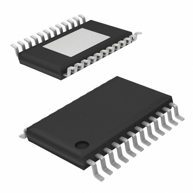


 工商网监
湘ICP备2023018690号
工商网监
湘ICP备2023018690号
