LT6018
33V, Ultralow Noise,
Precision Op Amp
Features
Description
Ultralow Voltage Noise
nn 30nV
P-P Noise: 0.1Hz to 10Hz
nn 1.2nV/√Hz Typical at 1kHz
nn Maximum Offset Voltage: 50μV
nn Maximum Offset Voltage Drift: 0.5μV/°C
nn CMRR: 124dB (Minimum)
nn A
VOL: 132dB (Minimum)
nn Slew Rate: 30V/μs
nn Gain-Bandwidth Product: 15MHz
nn Wide Supply Range: 8V to 33V
nn Ultralow THD: –115dB at 1kHz
nn Unity Gain Stable
nn Low Power Shutdown: 6.2µA
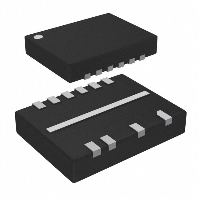
nn SO-8E and 4mm × 3mm 12-Lead DFN Packages
nn 4.5kV HBM and 2kV CDM Tolerant
The LT®6018 is a 33V precision operational amplifier
with excellent noise performance. With 0.1Hz to 10Hz
noise of only 30nVP-P, the LT6018 is an outstanding
choice for applications where 1/f noise impacts system
performance. The LT6018 has excellent DC performance
with a maximum offset voltage of 50µV and a maximum
offset voltage drift of 0.5µV/°C. The input offset voltage
remains low over the entire common mode input range,
providing a minimum CMRR of 124dB. Open loop gain
is typically 142dB enabling the part to achieve linearity
better than 1ppm. The proprietary circuit topology of the
LT6018 provides excellent slew rate and settling time
without compromising noise or DC precision.
nn
Applications
ADC Driver Applications
Low Noise Precision Signal Processing
nn Multiplexed Applications
nn DAC Buffer
nn Precision Data Acquisition
nn Active Filters
nn Professional Audio
nn
nn
An enable pin allows the LT6018 to be put in a low power
shutdown mode, reducing the typical supply current to
only 6.2µA. A reference pin for the enable pin is also
provided, which simplifies the interface between external
circuitry and the LT6018.
The LT6018 is available in 8-lead SO and 12-lead 4mm
× 3mm DFN packages, both of which include an exposed pad to reduce thermal resistance. The LT6018 is
specified over the –40°C to 85°C and –40°C to 125°C
temperature ranges.
L, LT, LTC, LTM, Linear Technology and the Linear logo are registered trademarks of Linear
Technology Corporation. All other trademarks are the property of their respective owners.
Typical Application
Precision Low Noise Buffer
V+
0.1Hz to 10Hz Voltage Noise
10µF
0.1µF
10nV/DIV
–
VIN
EN = V+
DGND = V–
+
LT6018
30nVP-P
VOUT
0.1µF
1s/DIV
10µF
V–
6018 TA01b
6018 TA01a
6018fa
For more information www.linear.com/LT6018
1
�LT6018
Absolute Maximum Ratings
(Note 1)
Total Supply Voltage (V+ to V–)..................................36V
Input Voltage
(+IN, –IN, DGND, EN).......... (V– – 0.3V) to (V+ + 0.3V)
Input Current (+IN, –IN, DGND, EN)...................... ±10mA
Differential Input Current (+IN, –IN)......................±25mA
Output Current (Note 2)................................... 50mARMS
Output Short-Circuit Duration..............Thermally Limited
Operating and Specified Temperature Range
I-Grade.................................................–40°C to 85°C
H-Grade.............................................. –40°C to 125°C
Maximum Junction Temperature........................... 150°C
Storage Temperature Range................... –65°C to 150°C
S8E Lead Temperature (Soldering, 10 sec)............ 300°C
Pin Configuration
TOP VIEW
TOP VIEW
DGND 1
–IN 2
+IN 3
8
9
V– 4
V+
6
OUT
NC
S8E PACKAGE
8-LEAD PLASTIC SO
θJA = 36°C/W, θJC = 9°C/W
EXPOSED PAD (PIN 9) MUST BE CONNECTED TO V– OR FLOATED
SEE "PIN FUNCTIONS” FOR DETAILS
NC IS NOT INTERNALLY CONNECTED
Order Information
1
12 DGND
V+
3
9
+IN
OUT
5
8
NC
NC
6
7
V–
11 NC
EN
7
5
EN
13
10 –IN
DE12(10) PACKAGE
12(10)-LEAD (4mm × 3mm) PLASTIC DFN
θJA = 43°C/W, θJC = 12°C/W
EXPOSED PAD (PIN 13) MUST BE CONNECTED TO V– OR FLOATED
SEE "PIN FUNCTIONS” FOR DETAILS
NC IS NOT INTERNALLY CONNECTED
PINS 2 AND 4 ARE REMOVED
http://www.linear.com/product/LT6018#orderinfo
LEAD FREE FINISH
TAPE AND REEL
PART MARKING*
PACKAGE DESCRIPTION
TEMPERATURE RANGE
LT6018IS8E#PBF
LT6018IS8E#TRPBF
6018
8-Lead Plastic S8E Exposed Pad
–40°C to 85°C
LT6018IDE#PBF
LT6018IDE#TRPBF
6018
12-Lead (4mm × 3mm) Plastic DFN
–40°C to 85°C
LT6018HS8E#PBF
LT6018HS8E#TRPBF
6018
8-Lead Plastic S8E Exposed Pad
–40°C to 125°C
LT6018HDE#PBF
LT6018HDE#TRPBF
6018
12-Lead (4mm × 3mm) Plastic DFN
–40°C to 125°C
Consult LTC Marketing for parts specified with wider operating temperature ranges. *The temperature grade is identified by a label on the shipping container.
For more information on lead free part marking, go to: http://www.linear.com/leadfree/
For more information on tape and reel specifications, go to: http://www.linear.com/tapeandreel/. Some packages are available in 500 unit reels through
designated sales channels with #TRMPBF suffix.
6018fa
2
For more information www.linear.com/LT6018
�LT6018
Electrical Characteristics
The l denotes the specifications which apply over the full operating
temperature range, otherwise specifications and all typical values are at TA = 25°C. V+ = 15V, V– = –15V, VCM = VOUT = 0V, VEN = 1.7V,
VDGND = 0V unless otherwise noted. VS is defined as (V+ – V–).
SYMBOL
VOS
PARAMETER
Input Offset Voltage
CONDITIONS
S8E Package
MIN
TYP
±7
l
±8
DFN Package
l
Long Term Input Offset Voltage
Stability (Note 3)
∆VOS/∆Temp Input Offset Voltage Drift (Note 4) S8E Package
DFN Package
Input Offset Current
IOS
l
l
l
en
Input Bias Current
Input Noise Voltage
Input Noise Voltage Density
CIN
Input Noise Current Density
Input Capacitance
RIN
Input Resistance
VICM
Common-Mode Input Range
(Note 5)
Common-Mode Rejection Ratio
in
CMRR
TA = –40°C to 85°C
TA = –40°C to 125°C
0.1Hz to 10Hz
f = 10Hz
f = 1kHz
f = 10kHz, Unbalanced Source
f = 10kHz, Balanced Source
Common Mode
Differential Mode
Common Mode
Differential Mode
Guaranteed by CMRR
l
l
Power Supply Rejection Ratio
l
VICM = –12V to 12V
VS = 8V to 33V
l
AVOL
Large-Signal Voltage Gain
RL = 500Ω, VOUT = –10V to 10V
l
VOL
Output Swing Low (VOUT – V–)
–50
–60
–150
–400
–900
±0.2
±0.2
±6
–60
V– + 3
124
120
130
128
132
128
No Load
ISINK = 1mA
133
140
142
80
100
750
ISINK = 20mA
l
Output Swing High (V+ – VOUT)
No Load
ISOURCE = 1mA
425
730
l
1150
ISOURCE = 20mA
l
ISC
SR
Short-Circuit Current
Slew Rate
VOUT = 0V, Sourcing
VOUT = 0V, Sinking
AV = 1, 10V Step
l
l
l
GBW
VS
Gain-Bandwidth Product
Supply Voltage Range
AV = 1, 5V Step
f = 50kHz
TA = –40°C to 85°C
TA = –40°C to 125°C
Guaranteed by PSRR
µV/°C
µV/°C
nA
nA
nA
nA
nA
nVP-P
nV/√Hz
nV/√Hz
pA/√Hz
pA/√Hz
pF
pF
MΩ
kΩ
V
V+ – 3
l
VOH
±0.5
±0.5
50
60
150
400
900
30
1.2
1.2
3
0.75
7
32
50
30
l
PSRR
UNITS
µV
µV
µV
µV
µV/Mo
0.45
∆VOS/∆Time
IB
MAX
±50
±75
±70
±95
l
l
l
40
65
20
15
12
11
9
8
200
700
1400
1800
800
900
1400
1600
90
100
30
20
15
33
dB
dB
dB
dB
dB
dB
mV
mV
mV
mV
mV
mV
mV
mV
mV
mV
mA
mA
V/µs
V/µs
V/µs
MHz
MHz
MHz
V
6018fa
For more information www.linear.com/LT6018
3
�LT6018
Electrical Characteristics
The l denotes the specifications which apply over the full operating
temperature range, otherwise specifications and all typical values are at TA = 25°C. V+ = 15V, V– = –15V, VCM = VOUT = 0V, VEN = 1.7V,
VDGND = 0V unless otherwise noted. VS is defined as (V+ – V–).
SYMBOL
IS
PARAMETER
Supply Current
CONDITIONS
In Active Mode
TA = –40°C to 85°C
TA = –40°C to 125°C
In Shutdown Mode, VEN = 0.8V
MIN
TYP
7.2
l
l
6.2
l
THD
Total Harmonic Distortion
tS
Settling Time
tON
VDGND
IDGND
IEN
VENL
VENH
Enable Time
DGND Pin Voltage Range
DGND Pin Current
EN Pin Current
EN Pin Input Low Voltage
EN Pin Input High Voltage
RL = 600Ω, f = 1kHz, VOUT = 3VRMS, AV = 1
RL = 600Ω, f = 10kHz, VOUT = 3VRMS, AV = 1
RL = 600Ω, f = 1kHz, VOUT = 20VP-P, AV = 1
RL = 600Ω, f = 10kHz, VOUT = 20VP-P , AV = 1
5V Step 0.0015% (16-Bit), AV = 1, RL = 2k, CL = 100pF
10V Step 0.0015% (16-Bit) , AV = 1, RL = 2k, CL = 100pF
AV = 1, Settled to 1%
–115
–104
–106
–92
1.2
1.2
25
l
V–
–700
–700
l
l
Relative to DGND
Relative to DGND
MAX
7.65
9
10
20
50
l
l
V+ – 3
–1400
–1400
0.8
1.7
UNITS
mA
mA
mA
µA
µA
dB
dB
dB
dB
µs
µs
μs
V
nA
nA
V
V
Electrical Characteristics
The l denotes the specifications which apply over the full operating
temperature range, otherwise specifications and all typical values are at TA = 25°C. V+ = 5V, V– = –5V, VCM = VOUT = 0V, VEN = 1.7V,
VDGND = 0V unless otherwise noted. VS is defined as (V+ – V–).
SYMBOL
VOS
PARAMETER
Input Offset Voltage
CONDITIONS
S8E Package
MIN
TYP
±7
l
±8
DFN Package
l
∆VOS/∆Temp Input Offset Voltage Drift (Note 4)
IOS
S8E Package
DFN Package
l
l
Input Offset Current
l
IB
en
Input Bias Current
Input Noise Voltage
Input Noise Voltage Density
CIN
Input Noise Current Density
Input Capacitance
RIN
Input Resistance
VICM
CMRR
Common-Mode Input Range (Note 5)
Common-Mode Rejection Ratio
in
TA = –40°C to 85°C
TA = –40°C to 125°C
0.1Hz to 10Hz
f = 10Hz
f = 1kHz
f = 10kHz, Unbalanced Source
f = 10kHz, Balanced Source
Common Mode
Differential Mode
Common Mode
Differential Mode
Guaranteed by CMRR
VICM = –2V to 2V
l
l
–50
–60
–150
–400
–900
±0.2
±0.2
±6
–40
MAX
±50
±75
±70
±95
±0.5
±0.5
50
60
150
400
900
30
1.2
1.2
3
0.75
8.3
39
50
30
l
l
V– + 3
122
118
V+ – 3
130
UNITS
µV
µV
µV
µV
µV/°C
µV/°C
nA
nA
nA
nA
nA
nVP-P
nV/√Hz
nV/√Hz
pA/√Hz
pA/√Hz
pF
pF
MΩ
kΩ
V
dB
dB
6018fa
4
For more information www.linear.com/LT6018
�LT6018
Electrical Characteristics
The l denotes the specifications which apply over the full operating
temperature range, otherwise specifications and all typical values are at TA = 25°C. V+ = 5V, V– = –5V, VCM = VOUT = 0V, VEN = 1.7V,
VDGND = 0V unless otherwise noted. VS is defined as (V+ – V–).
PSRR
Power Supply Rejection Ratio
VS = 8V to 33V
l
AVOL
Large-Signal Voltage Gain
RL = 500Ω, VOUT = –2V to 2V
l
VOL
Output Swing Low (VOUT – V–)
130
128
130
126
No Load
ISINK = 1mA
140
142
80
100
l
900
ISINK = 20mA
l
VOH
Output Swing High (V+ – VOUT)
No Load
ISOURCE = 1mA
425
700
l
1160
ISOURCE = 20mA
l
ISC
Short-Circuit Current
SR
Slew Rate
GBW
Gain-Bandwidth Product
VS
IS
Supply Voltage Range
Supply Current
VOUT = 0V, Sourcing
VOUT = 0V, Sinking
AV = 1, 4V Step
AV = 1, 2V Step
f = 50kHz
TA = –40°C to 85°C
TA = –40°C to 125°C
Guaranteed by PSRR
In Active Mode
TA = –40°C to 85°C
TA = –40°C to 125°C
In Shutdown Mode, VEN = 0.8V
l
l
l
l
l
40
40
11.5
10.5
8.5
8
Total Harmonic Distortion
6.6
l
l
6
tON
VDGND
IDGND
IEN
VENL
VENH
Enable Time
DGND Pin Voltage Range
DGND Pin Current
EN Pin Current
EN Pin Input Low Voltage
EN Pin Input High Voltage
RL = 100Ω, f = 1kHz, VOUT = 1.41VRMS, AV = 1
RL = 100Ω, f = 10kHz, VOUT = 1.41VRMS, AV = 1
AV = 1, Settled to 1%
V–
–700
–700
l
l
Note 1: Stresses beyond those listed under Absolute Maximum Ratings
may cause permanent damage to the device. Exposure to any Absolute
Maximum Rating condition for extended periods may affect device
reliability and lifetime.
Note 2: The LT6018 is capable of producing peak output currents in
excess of 50mA. Current density limitations within the IC require the
continuous RMS current supplied by the output (sourcing or sinking)
over the operating lifetime of the part be limited to under 50mA (Absolute
Maximum). Proper heat sinking may be required to keep the junction
temperature below the absolute maximum rating. Refer to Figure 9, and
the Safe Operating Area section of the data sheet for more information.
33
7
8.5
9.5
20
50
–107
–86
35
l
Relative to DGND
Relative to DGND
800
900
1400
1600
85
60
13
10
14.5
l
THD
200
700
1400
1800
l
l
1.7
V+ – 3
–1400
–1400
0.8
dB
dB
dB
dB
mV
mV
mV
mV
mV
mV
mV
mV
mV
mV
mA
mA
V/µs
V/µs
MHz
MHz
MHz
V
mA
mA
mA
µA
µA
dB
dB
μs
V
nA
nA
V
V
Note 3: Long term input offset voltage stability refers to the average trend
line of offset voltage vs time over extended periods after the first 30 days
of operation.
Note 4: Guaranteed by design.
Note 5: The LT6018 input stage is limited to operating between V– + 3V
and V+ – 3V. Exceeding this input common mode range will cause a
significant increase in input bias current, reduction of open loop gain and
degraded stability.
6018fa
For more information www.linear.com/LT6018
5
�LT6018
Typical Performance Characteristics
TA = 25°C, V+ = 15V, V– = –15V, VEN = 1.7V, VDGND = 0V, RL = 500Ω unless otherwise noted.
Typical Distribution of Input
Offset Voltage
50
45
40
35
30
25
20
15
10
30
5526 PARTS
DFN PACKAGE
35
30
25
20
15
10
5
5
0
–40 –32 –24 –16 –8 0 8 16 24 32 40
INPUT OFFSET VOLTAGE (µV)
0
–40 –32 –24 –16 –8 0 8 16 24 32 40
INPUT OFFSET VOLTAGE (µV)
6018 G01
15
10
5
0
–0.5 –0.4 –0.3 –0.2 –0.1 0.0 0.1 0.2
INPUT OFFSET VOLTAGE DRIFT (µV/°C)
123 PARTS
DFN PACKAGE
20
15
10
5
0
–0.4 –0.3 –0.2 –0.1 0.0 0.1 0.2 0.3
INPUT OFFSET VOLTAGE DRIFT (µV/°C)
Input Offset Voltage
vs Supply Voltage
20
SOIC–8E PACKAGE
5 TYPICAL PARTS
5 TYPICAL PARTS
15
6018 G05
10s/DIV
10
5
0
–5
–10
–15
–20
0.4
0
4
8 12 16 20 24 28
TOTAL SUPPLY VOLTAGE (V)
6018 G04
36
Input Bias Current vs Temperature
5
50
4
0
3
–50
INPUT BIAS CURRENT (nA)
INPUT OFFSET VOLTAGE (µV)
32
6018 G06
Input Offset Voltage vs
Input Common Mode Voltage
2
1
0
–1
–2
–3
–4
–5
–15
0.3
6018 G03
Input Offset Voltage
Warm-Up Drift
CHANGE IN OFFSET VOLTAGE (2µV/DIV)
PERCENTAGE OF UNITS (%)
25
20
6018 G02
Typical Distribution of Input
Offset Voltage Drift
30
128 PARTS
SOIC–8E PACKAGE
25
40
PERCENTAGE OF UNITS (%)
6033 PARTS
SOIC–8E PACKAGE
PERCENTAGE OF UNITS (%)
PERCENTAGE OF UNTIS (%)
45
Typical Distribution of Input
Offset Voltage Drift
INPUT OFFSET VOLTAGE (µV)
50
Typical Distribution of Input
Offset Voltage
5 TYPICAL PARTS
–100
–150
–200
–250
–300
–350
–400
–450
–10
–5
0
5
10
INPUT COMMON MODE VOLTAGE (V)
15
–500
–50
–25
6018 G09
0
25
50
75
TEMPERATURE (°C)
100
125
6018 G10
6018fa
6
For more information www.linear.com/LT6018
�LT6018
Typical Performance Characteristics
TA = 25°C, V+ = 15V, V– = –15V, VEN = 1.7V, VDGND = 0V, RL = 500Ω unless otherwise noted.
Open-Loop Gain and Phase
vs Frequency
Open-Loop Gain vs Load
150
0
160
OPEN LOOP GAIN (dB)
100
–90
80
60
–135
40
20
OPEN LOOP PHASE (DEGREES)
–45
120
OPEN LOOP GAIN (dB)
140
VOUT = ±10V
145
140
135
–180
0
–20
0.1
1
10 100 1k 10k 100k 1M 10M100M
FREQUENCY (Hz)
130
0.1
1
10
LOAD CURRENT (mA)
100
6018 G08
6018 G07
Voltage Noise Density
vs Frequency
0.1Hz to 10Hz Voltage Noise
Integrated Voltage Noise
(0.1Hz to Frequency Indicated)
6018 G11
1s/DIV
10
RMS VOLTAGE NOISE (µV)
10nV/DIV
VOLTAGE NOISE DENSITY (nV/√Hz)
100
10
1
0.1
0.1
1
10 100 1k 10k 100k 1M 10M100M
FREQUENCY (Hz)
1
0.1
0.01
0.001
1
10
100 1k 10k 100k
FREQUENCY (Hz)
Current Noise Density
vs Frequency
CURRENT NOISE DENSITY (pA/√Hz)
1k
100
10
UNBALANCED
BALANCED
1
0.1
0.1
1
10
100 1k 10k 100k
FREQUENCY (Hz)
1M
MAXIMUM UNDISTORTED OUTPUT VOLTAGE (VP-P)
6018 G12
1M
10M
6018 G13
Maximum Undistorted Output
Amplitude vs Frequency
30
25
AV = 1
THD < –40dB
20
15
10
5
0
0.01
0.1
6018 G14
1
10
FREQUENCY (kHz)
100
1000
6018 G15
6018fa
For more information www.linear.com/LT6018
7
�LT6018
Typical Performance Characteristics
TA = 25°C, V+ = 15V, V– = –15V, VEN = 1.7V, VDGND = 0V, RL = 500Ω unless otherwise noted.
Large-Signal Transient Response
(5V Step)
Large-Signal Transient Response
(10V Step)
AV = 1
Small-Signal Transient Response
560pF
AV = 1
AV = 1
100pF
0pF
1V/DIV
2V/DIV
6018 G16
1µs/DIV
Overshoot vs Capacitive Load
Vs = ±15V
30
20
100
AV = 1
90
35
30
25
10
–50
0 100 200 300 400 500 600 700 800 900 1000
CAPACITIVE LOAD (pF)
–25
0
25
50
75
TEMPERATURE (°C)
100
FALLING EDGE
80
RISING EDGE
40
0
5
50
40
30
RISING EDGE
125
0
–50
–25
0
25
50
75
TEMPERATURE (°C)
100
125
6018 G21
CMRR vs Frequency
120
0
60
160
COMMON MODE REJECTION RATIO (dB)
SLEW RATE (V/µs)
160
FALLING EDGE
70
6018 G20
Slew Rate vs Input Step
AV = 1
VS = ±18V
AV = 1
10
6018 G19
200
Slew Rate vs Temperature
(10V Step)
20
RISING EDGE
15
6018 G18
80
FALLING EDGE
20
10
0
Slew Rate vs Temperature
(5V Step)
40
50
40
100ns/DIV
45
Vs = ±5V
SLEW RATE (V/µs)
OVERSHOOT (%)
50
AV = 1
60
6018 G17
1µs/DIV
SLEW RATE (V/µs)
70
5mV/DIV
10
15
20
25
INPUT STEP SIZE (VP–P)
30
140
120
100
80
60
40
20
0
1k
6018 G22
10k
100k
1M
FREQUENCY (Hz)
10M
100M
6018 G23
6018fa
8
For more information www.linear.com/LT6018
�LT6018
Typical Performance Characteristics
TA = 25°C, V+ = 15V, V– = –15V, VEN = 1.7V, VDGND = 0V, RL = 500Ω unless otherwise noted.
160
POWER SUPPLY REJECTION RATIO (dB)
CL = 100pF
AV = 1
GAIN(dB)
0
–3
CL = 0pF
AV = 1
–6
CL = 100pF
AV = –1
RF = 300Ω
–9
–12
0.01
0.1
1
10
FREQUENCY (MHz)
PSRR vs Frequency
140
120
–PSRR
100
80
+PSRR
60
40
20
0
0.1
100
1
10 100 1k 10k 100k 1M 10M100M
FREQUENCY (Hz)
VOUT = 3VRMS
RF = 1k
RL = 600Ω
RL = 2kΩ
–100
–105
RL = 2kΩ
–110
–115
–120
1
10
FREQUENCY (kHz)
Supply Current vs Supply Voltage
45
40
35
30
25
20
125°C
15
10
5
1
10
FREQUENCY (kHz)
–12–10 –8 –6 –4 –2 0 2 4 6
INPUT VOLTAGE(V)
100
8 10 12
Shutdown Supply Current
vs Temperature
85°C
0
5
25°C
10
15
20
SUPPLY VOLTAGE (V)
–40°C
25
30
6018 G31
Enable/Disable Response
AV = 1
11
VEN
0V
5V/DIV
VOUT
0V
5V/DIV
VS = 30V
10
9
8
7
VIN = 10Vp–p AT 70kHz
I(V+)
0A
5mA/DIV
VS = 10V
6
100µs/DIV
5
4
–50
0
6018 G28
6018 G27
12
100
6018 G26
50
–110
–115
RL = 600Ω
–105
SUPPLY CURRENT (mA)
–95
VOUT = 3VRMS
–100
RLOAD = 600Ω
AV = 1
–90
THD + Noise vs Frequency, AV = 1
–95
DC Linearity
OUTPUT ERROR (1ppm/DIV)
–85
–90
6018 G27
THD + Noise vs Frequency,
AV = –1
SHUTDOWN SUPPLY CURRENT (µA)
TOTAL HARMONIC DISTORTION + NOISE (dB)
6018 G26
–80
TOTAL HARMONIC DISTORTION + NOISE (dB)
Closed Loop Gain vs Frequency
3
–25
0
25
50
75
TEMPERATURE (°C)
100
6018 G33
125
6018 G32
6018fa
For more information www.linear.com/LT6018
9
�LT6018
Typical Performance Characteristics
TA = 25°C, V+ = 15V, V– = –15V, VEN = 1.7V, VDGND = 0V, RL = 500Ω unless otherwise noted.
2.0
OUTPUT HIGH SATURATION VOLTAGE (V)
OUTPUT LOW SATURATION VOLTAGE (V)
1.0
Output Saturation Voltage
vs Sink Current (Output Low)
0.9
0.8
85°C
0.7
0.6
125°C
0.5
25°C
0.4
–40°C
0.3
0.2
0.1
0
0
2
4 6 8 10 12 14 16 18 20
SINKING LOAD CURRENT (mA)
Output Saturation Voltage
vs Source Current (Output High)
1.8
1.6
–40°C
1.4
25°C
1.2
1.0
0.8
0.6
0.4
85°C
0.2
0
125°C
0
2
4 6 8 10 12 14 16 18 20
SOURCING LOAD CURRENT (mA)
6018 G34
6018 G35
Positive Output Overdrive
Recovery
Negative Output Overdrive
Recovery
AV = –100
AV = –100
OUTPUT
5V/DIV
INPUT
200mV/DIV
0V
0V
OUTPUT
5V/DIV
INPUT
200mV/DIV
4µs/DIV
6018 G36
4µs/DIV
6018 G37
6018fa
10
For more information www.linear.com/LT6018
�LT6018
Pin Functions
(SOIC-8E/DFN)
DGND (Pin 1/Pins 12): Reference for EN Pin. It is normally
tied to ground. DGND must be in the range from V– to
V+ – 3V. If grounded, V+ must be ≥3V. The EN pin threshold
is specified with respect to the DGND pin. DGND cannot
be floated.
V+ (Pin 7/Pin 3): Positive Power Supply. Bypass capacitors should be placed as close as possible between the
LT6018 supply pins and ground to ensure proper bypassing. Additional bypass capacitance may be used between
the power supply pins.
–IN (Pin 2/Pin 10): Inverting Input of the Amplifier.
EN (Pin 8/Pin 1): Enable Input. This pin must be connected
high, normally to V+, for the amplifier to be functional.
EN is active high with the threshold approximately two
diodes above DGND. EN cannot be floated. The shutdown
threshold voltage is specified with respect to the voltage
on the DGND pin.
+IN (Pin 3/Pin 9): Noninverting Input of the Amplifier.
V– (Pin 4/Pin 7): Negative Power Supply. Bypass capacitors should be placed as close as possible between the
LT6018 supply pins and ground to ensure proper bypassing. Additional bypass capacitance may be used between
the power supply pins.
OUT (Pin 6/Pin 5): Amplifier Output. In shutdown mode,
the amplifier’s output is not high impedance (see Applications section).
NC (Pin 5/Pins 6, 8, 11): Not internally connected.
Exposed Pad (Pin 9/Pin 13): The exposed pad is electrically connected to V–, but should not be used to provide
power to the part. Use the V– pin to provide power. The
exposed pad can be connected to V– or floated. Connecting the exposed pad to the V– plane will improve thermal
performance (see Safe Operating Area section).
Simplified Schematic
V+
LOAD
+IN
–IN
2.8Ω
2.8Ω
OUTPUT
DRIVE
CIRCUITRY
OUT
EN
50k
50k
DGND
V–
6018 SS
6018fa
For more information www.linear.com/LT6018
11
�LT6018
Applications Information
Overview
Noise
The proprietary circuitry used in the LT6018 provides a
unique combination of precision specifications including
ultralow 1/f noise, low broadband noise, low offset and
enhanced slew rate without degrading CMRR. The combination of DC specifications and fast settling time allows
the LT6018 to solve demanding signal chain requirements.
Attention to board layout, supply bypassing and heat sinking must be observed to ensure that the full performance
of the LT6018 is realized.
The amplifier voltage noise (en), positive input current noise
(inp), negative input current noise (inn), source resistance
(RS), and feedback resistors (R1) and (R2) are individual
voltage noise contributors. The total noise (enot) appearing
at the output of the LT6018 will be the root sum square
of all the individual voltage noise contributors (Figure 1).
2
2
2
2
2
2
enot = eno
+erso
+einpo
+er1o
+er2o
+einno
R2
Gv = 1+
R1
eno = en •GV
The supply current of the LT6018 increases with large differential input voltages. Normally, this does not impact the
LT6018 because the amplifier is forcing the two inputs to
be at the same potential. Conditions which cause continuous differential input voltage to appear should be avoided
in order to avoid excessive die heating of the LT6018. This
includes but is not limited to: operation as a comparator,
excessive loading on the output and overdriving the input.
Preserving Input Precision
Preserving the input accuracy of the LT6018 requires
that the application circuit and PC board layout do not
introduce errors comparable to or greater than the 7µV
typical offset of the amplifier. Temperature differentials
across the input connections can generate thermocouple
voltages of tens of microvolts so the connections of the
input leads should be short, close together and away from
heat dissipating components. Air currents across the board
can also generate temperature differentials.
In precision applications it is also important to consider
amplifier loading when selecting feedback resistor values
as well as the loads on the device as these will appear in
parallel and affect input offset. See the Feedback Components section for more details.
erso = enrs •GV = 4kTRS •GV
einpo =inp •RS •GV
R2
R2
= 4kTR1•
R1
R1
er2o = enr2 = 4kTR2
er1o = enr1 •
einno =inn •R2
The total input referred voltage noise (enit) is calculated
by dividing the total output referred voltage noise (enot)
by the amplifier gain.
enit =
enot
GV
R1
enr1
R2
enr2
inn
–
inp
LT6018
+
RS
enrs
6018 F01
enot
en
Figure 1. LT6018 Noise Contributors
6018fa
12
For more information www.linear.com/LT6018
�LT6018
Applications Information
150
Op amps often have protection diodes clamping the two
inputs within a diode voltage of each other as seen in
Figure 2. During large voltage transitions on the input,
these diodes can conduct, since the output cannot respond
instantaneously. This can cause circuitry in front of the
amplifier as well as the amplifier’s own output stage to
get overloaded. Often there may be series input resistors
(either integrated or discrete) to limit this current, but
on extremely low noise parts such as the LT6018, that
is not desirable.
120
The unique input circuitry of the LT6018 does not have
this typical diode configuration, but rather a series Zener
diode configuration as shown in Figure 3. For 5V input
steps, the LT6018 has much higher impedance during
transients and allows the user to reduce or eliminate the
current limiting resistors, preserving low noise. Figure 4
shows how input bias current increases with differential
input voltage for the traditional protection scheme and the
LT6018 protection scheme.
CURRENT LIMITING RESISTOR NEEDED
RF
–
OUTPUT
6018 F02
5V INPUT STEP
+
Figure 2. Typical Op Amp Diode Input Protection
CURRENT LIMITING RESISTOR NOT NEEDED
–
LT6018
OUTPUT
6018 F03
5V INPUT STEP
INPUT BIAS CURRENT (µA)
High Dynamic Input Impedance
90
60
LT6018 IB–
LT6018 IB+
30
0
–30
–60
–90
–120
–150
TYPICAL
OP AMP IB+
TYPICAL
OP AMP IB–
–6 –5 –4 –3 –2 –1 0 1 2 3 4 5
DIFFERENTIAL INPUT VOLTAGE (V)
6
6018 F04
Figure 4. Typical Op Amp vs LT6018 Input Protection
Shutdown Operation
The LT6018 shutdown function has been designed to
be easily controlled from single supply logic or microcontrollers. To enable the LT6018 when VDGND = 0V the
enable pin must be driven above 1.7V. Conversely, to
enter the low power shutdown mode the enable pin must
be driven below 0.8V. In a ±15V dual supply application
where VDGND = –15V, the enable pin must be driven above
–13.3V to enable the LT6018. If the enable pin is driven
below –14.2V the LT6018 enters the low power shutdown
mode. Note that to enable the LT6018 the enable pin voltage can range from –13.3V to 15V whereas to disable the
LT6018 the enable pin can range from –15V to –14.2V.
Figure 5 shows examples of enable pin control. While in
shutdown, the output of the LT6018 is not high impedance. The LT6018 is typically capable of coming out of
shutdown within 25μs. This is useful in power sensitive
applications where duty cycled operation is employed. In
these applications the system is in low power mode the
majority of the time, but then needs to wake up quickly
and settle for an acquisition before being powered back
down to save power.
+
Figure 3. LT6018 Series Zener Diode Input Protection
6018fa
For more information www.linear.com/LT6018
13
�LT6018
Applications Information
–13.3V TO 15V
1.7V TO 15V
ON
–15V TO –14.2V
15V
15V
–
+
OR
EN TO V
EN LOGIC
+
LT6018
30V
LT6018
DGND
–15V
HIGH VOLTAGE
SPLIT SUPPLIES
–
–
OFF
8V
–
LT6018
–
DGND
–15V
HIGH VOLTAGE
SPLIT SUPPLIES
+
OR
EN TO V
EN LOGIC
+
LT6018
DGND
OFF
4V
+
OR
EN TO V
EN LOGIC
+
LT6018
DGND
–4V TO –3.2V
0V TO 0.8V
OFF
+
OR
EN TO V
EN LOGIC
+
ON
ON
0V TO 0.8V
OFF
–2.3V TO 4V
1.7V TO 8V
ON
OV TO 0.8V
OFF
+
OR
EN TO V
EN LOGIC
+
1.7V TO 30V
ON
DGND
–4V
HIGH VOLTAGE
SINGLE SUPPLY
LOW VOLTAGE
SPLIT SUPPLIES
LOW VOLTAGE
SINGLE SUPPLY
6018 F05
Figure 5. LT6018 Enable Pin Control Examples
Output Leakage in Shutdown Mode
ILEAKAGE
–
+15V
6018 F06
+
VOUT
–15V
Figure 6. Output Leakage in Shutdown Mode
10
8
6
4
ILEAKAGE (µA)
In shutdown mode, the LT6018’s output is not high impedance and may conduct a small amount of current due to
on-chip leakages. This current can interact with the input
protection diodes or any other circuitry connected to the
output. Consider the case of a unity gain buffer shown in
Figure 6. When the LT6018 is placed in shutdown mode,
leakage current flows from the VOUT pin through the input
protection diodes causing VOUT to be around 6V. If the
output pin is loaded to ground in the same example, the
output would be ILEAKAGE • RLOAD above ground. Figure 7
shows the resulting current as the VOUT is swept. In addition, transient voltage applied to the LT6018 output
while in shutdown mode may cause the output devices
to momentarily conduct.
–40°C
2
25°C
0
–2
90°C
–4
Feedback Components
To optimize the stability and noise performance of the
LT6018, care must be taken when selecting feedback
components. For higher resistance values, the pole formed
by the inverting parasitic input capacitance and feedback
resistors will tend to degrade stability; a lead compensation capacitor across the feedback resistor may be used
to eliminate ringing or oscillation. Larger value feedback
–6
125°C
–8
–10
–8
–6
–4
–2
0
2
4
APPLIED VOUT(V)
6
8
6018 F07
Figure 7. Output Impedance in Shutdown Mode
Configured as a Buffer
6018fa
14
For more information www.linear.com/LT6018
�LT6018
Applications Information
CF
GAIN
RG
RF
CF
RTI NOISE, f = 1kHz
(nV/√Hz)
2.48
3.46
5.20
2.08
1.73
1.27
1.23
1.51
2 500Ω 500Ω
2
5pF
1k
1k
2
5pF
2k
2k
5 200Ω 800Ω
10 100Ω 900Ω
101 10Ω
1k
201 5Ω
1k
201 50Ω 10k
RF
–
RG
CPAR
LT6018
VOUT
+
6018 F08
Figure 8. Suggested Feedback Components for Low Noise Stable Operation
resistors will also contribute more thermal noise and
further degrade performance (see Applications Information, Noise section). Lower value resistances will tend to
improve on these conditions, however, excessive amplifier
loading may occur as the feedback network will appear in
parallel with the load resistance the LT6018 is required to
drive. Figure 8 shows suggested feedback components for
maintaining good loop stability and noise performance.
Capacitive Loads
The LT6018 can easily drive capacitive loads up to 100pF in
unity gain. The capacitive load driving capability increases
as the amplifier is used in higher gain configurations. A
small series resistance between the output and the load
further increases the amount of capacitance that the amplifier can drive.
60
The safe operating area, or SOA shown in Figure 9, illustrates
the voltage, current and temperature conditions where
the LT6018 can be reliably operated. The SOA takes into
account the ambient temperature and the power dissipated
by the device. This includes the product of the load current
and the difference between the supply and output voltage,
and the quiescent current and supply voltage.
The LT6018 is safe when operated within the boundaries
shown in Figure 9. Thermal resistance junction to case,
θJC, is rated at a constant 9°C/W. Thermal resistance junction to ambient θJA, is dependent on board layout and any
additional heat sinking. Connecting the exposed pad to
V– will reduce θJA and improve thermal performance. The
curves in Figure 9 show the direct effect of θJA on SOA.
CURRENT DENSITY LIMITED
55
50
LOAD CURRENT (mA)
Safe Operating Area
TA = 125°C
θJA = 36°C/W
45
40
θJA = 43°C/W
35
30
θJA = 50°C/W
25
20
15
10
5 JUNCTION TEMPERATURE LIMITED
0
0
5
10
15
20
25
SUPPLY VOLTAGE – LOAD VOLTAGE (V)
30
6018 F09
Figure 9. Safe Operating Area
6018fa
For more information www.linear.com/LT6018
15
�LT6018
Typical Applications
Low Noise, Low Distortion 5kHz Wien Bridge Oscillator with 3% Frequency Trim and Injection Lock
20k
68nF
FILM
3.24k
464Ω
15V
FREQ
TRIM
#327 BULB
28V
1W
511Ω
15V
EN
+
68nF
FILM
15V
+
OUT
LT6018
–
DGND
–15V
20Ω
49.9Ω
LT1206
–
200pF
–15V
10nF
649Ω
324Ω
OUT
S/D
HD2 = –131dBc
HD3 = –108dBc
432Ω*
* ADJUST FOR AMPLITUDE
100k
INJECTION
LOCK INPUT
FREQUENCY TRIM RANGE: ±3%
INJECTION LOCK: ±0.5% AT 5VPK DRIVE
INJECTION ATTENUATION: 41dB 2nd, 44dB 3rd
6018 TA02
Low Noise Extended Output Swing 1M TIA Photodiode Amplifier
+24V
6.19k
IPD
PHOTO
DIODE
SFH213
0.1µF
1M
D JFET
NXP
BF862
S
–
1.5k
–5V
–5V
EN = V +
0.5pF
LT6018
+
VOUT
~0.4V + IPD • 1M
VS = +24V/–5V
BW = 500kHz
DGND = V –
6018 TA03
6018fa
16
For more information www.linear.com/LT6018
�LT6018
Typical Applications
Low Noise Precision Current Monitor
R1
1k
+
V
RSENSE
0.01Ω
R11
10Ω
15V
+
–
–
+
VSENSE
15V
EN
LT6018
+
–
R2*
1k
15V
–
DGND
–15V
15V
LT1678
R3*
5k
VOUT
LT1678
+
R4*
1k
R5*
5k
–15V
VREF
*LT5400-6
–15V
THE LT6018 IN THIS CIRCUIT PROVIDES LOW NOISE, LOW DISTORTION AMPLIFICATION
OF A SMALL SENSE VOLTAGE DERIVED FROM A LOW IMPEDANCE SOURCE ACROSS A
WIDE INPUT COMMON MODE RANGE.
THE SECOND STAGE DIFFERENTIAL AMPLIFIER WITH VARIABLE REFERENCE REJECTS
THE INPUT COMMON MODE VOLTAGE.
AN OPTIONAL LT1678 BUFFER AMPLIFIER FURTHER ISOLATES THE SOURCE FROM
LOADING BY R4 AND R5.
THE GAIN IS 500V/V, WITH BANDWIDTH APPROXIMATELY 100kHz AND INPUT REFERRED
NOISE 1.45nV/√Hz.
6018 TA04
6018fa
For more information www.linear.com/LT6018
17
�LT6018
Typical Applications
Low Noise, High CMRR Instrumentation Amplifier
+15V
15V
15V
EN
V–IN
–REFA
–REFB
–REFC
19k
38k
23.75k
LT6018
V+
190k
DGND
49.9k
–15V
–IN 190k
OUT
49.9Ω
190k
VOUT
+IN
15V
15V
EN
190k
49.9k
REF
VREF
LT6018
DGND
V+IN
–15V
19k
38k
23.75k
+REFA
+REFB
+REFC
GAIN = 2000V/V
INPUT REFERRED NOISE = 2.1nV/√Hz
CMRR = 150dB
–3dB BANDWIDTH = 7.5kHz
SHDN
V–
LT6375
–15V
6018 TA05
6018fa
18
For more information www.linear.com/LT6018
�LT6018
Package Description
Please refer to http://www.linear.com/product/LT6018#packaging for the most recent package drawings.
S8E Package
8-Lead Plastic SOIC (Narrow .150 Inch) Exposed Pad
(Reference LTC DWG # 05-08-1857 Rev C)
.050
(1.27)
BSC
.189 – .197
(4.801 – 5.004)
NOTE 3
.045 ±.005
(1.143 ±0.127)
8
.089
.160 ±.005
(2.26) (4.06 ±0.127)
REF
.245
(6.22)
MIN
.150 – .157
.080 – .099
(2.032 – 2.530) (3.810 – 3.988)
NOTE 3
.228 – .244
(5.791 – 6.197)
1
.030 ±.005
(0.76 ±0.127)
TYP
.005 (0.13) MAX
7
5
6
.118
(2.99)
REF
3
2
.118 – .139
(2.997 – 3.550)
4
RECOMMENDED SOLDER PAD LAYOUT
.010 – .020
× 45°
(0.254 – 0.508)
.008 – .010
(0.203 – 0.254)
.053 – .069
(1.346 – 1.752)
0°– 8° TYP
.016 – .050
(0.406 – 1.270)
.014 – .019
(0.355 – 0.483)
TYP
NOTE:
1. DIMENSIONS IN
INCHES
(MILLIMETERS)
2. DRAWING NOT TO SCALE
3. THESE DIMENSIONS DO NOT INCLUDE MOLD FLASH OR PROTRUSIONS.
MOLD FLASH OR PROTRUSIONS SHALL NOT EXCEED .010" (0.254mm)
4.
STANDARD LEAD STANDOFF IS 4mils TO 10mils (DATE CODE BEFORE 542)
5.
LOWER LEAD STANDOFF IS 0mils TO 5mils (DATE CODE AFTER 542)
4
5
.004 – .010
0.0 – 0.005
(0.101 – 0.254) (0.0 – 0.130)
.050
(1.270)
BSC S8E 1015 REV C
6018fa
For more information www.linear.com/LT6018
19
�LT6018
Package Description
Please refer to http://www.linear.com/product/LT6018#packaging for the most recent package drawings.
DE12(10) Package
12-Lead Plastic DFN (4mm × 3mm)
Variation DE12(10) with 2 Pins Removed. Flip Chip
(Reference LTC DWG # 05-08-1971 Rev Ø)
0.70 ±0.05
0.25 ±0.05
3.55 ±0.05
3.60 ±0.05
2.10 ±0.05
2.20 ±0.05
PACKAGE OUTLINE
0.25 ±0.05
0.50 BSC
RECOMMENDED SOLDER PAD PITCH AND DIMENSIONS
APPLY SOLDER MASK TO AREAS THAT ARE NOT SOLDERED
0.40 ±0.10
4.00 ±0.10
(2 SIDES)
PIN 1
TOP MARK
(NOTE 5)
0.200 REF
7
3.00 ±0.10
(2 SIDES)
12
0.2 ±0.05
1.00
REF
3.55 ±0.10
0.50 ±0.05
0.75 ±0.05
6
1
0.25 ±0.05
(UE12(10) DFN 0314 REV O
0.50 BSC
BOTTOM VIEW—EXPOSED PAD
0.00 – 0.05
NOTE:
1. DRAWING NOT TO SCALE
2. ALL DIMENSIONS ARE IN MILLIMETERS
3. DIMENSIONS OF EXPOSED PAD ON BOTTOM OF PACKAGE DO NOT INCLUDE
MOLD FLASH. MOLD FLASH, IF PRESENT, SHALL NOT EXCEED 0.15mm ON ANY SIDE
4. EXPOSED PAD SHALL BE SOLDER PLATED
5. SHADED AREA IS ONLY A REFERENCE FOR PIN 1 LOCATION
ON THE TOP AND BOTTOM OF PACKAGE
6018fa
20
Information furnished by Linear Technology Corporation is believed to be accurate and reliable.
However, no responsibility is assumed for its use. Linear Technology Corporation makes no representation that the interconnection
of its circuits
as described
herein will not infringe on existing patent rights.
For more
information
www.linear.com/LT6018
�LT6018
Revision History
REV
DATE
DESCRIPTION
A
01/17
Product description changed from 36V to 33V
PAGE NUMBER
1
Package name description changed from SOIC to SO
1
Long Term Input Offset Voltage Stability added
3
Note 3 added for Long Term Input Offset Voltage Stability. Note 3 and Note 4 renamed Note 4 and Note 5,
respectively
5
6018fa
For more information www.linear.com/LT6018
21
�LT6018
Typical Applications
Driving LTC2378-20 with ±10V Input Signal (fIN = 100Hz, –1dBFS, 800ksps)
10V/AV
10V
–10V/AV
VIN
–10V
15V
15V
EN
+
LT6018
–
DGND
–15V
R
A V = 1+ F
RG
LT5400-4
1k
R1
C1
10k
RF
20k
RG
VREF = 5V
499Ω
+
1k
IN+
IN–
LT1637
5V
1k
5V
2.5V
VREF
VDD
LTC2378-20
SAR ADC
20-BIT
GND
6018 TA06
499Ω
10µF
AV (V/V)
0V
1k
+15V
–
20k
5V
–15V
COMPONENT VALUES
0V
SNR (dB)
THD (dB)
SFDR (dB)
1
RF = 0Ω, RG = OPEN, R1 = 0Ω, C1 = OPEN
102.5
–121.6
123.0
10
RF = 900Ω, RG = 100Ω, R1 = 10Ω, C1 = 0.01µF
100.6
–99.8
100.0
Related Parts
PART NUMBER DESCRIPTION
COMMENTS
LT1028
Ultralow Noise, Precision High Speed Op Amp, AV ≥ 2
Stable
0.1Hz to 10Hz Noise = 35nVP-P, en = 0.85nV/√Hz, VOS = 40µV, SR = 15V/µs,
GBW = 75MHz, IS = 7.4mA
LT1128
Ultralow Noise, Precision High Speed Op Amp ,
AV = +1 Stable
0.1Hz to 10Hz Noise = 35nVP-P, en = 0.85nV/√Hz, VOS = 40µV, SR = 6V/µs,
GBW = 20MHz, IS = 7.4mA
LT1115
Ultralow Noise, Low Distortion, Audio Op Amp
DC to 20kHz Noise = 0.5µVP-P, en = 0.9nV/√Hz, VOS = 200µV, SR = 15V/µs,
GBW = 70MHz, IS = 8.5mA
LT1037
Low Noise, High Speed Precision Op Amp , AV ≥ 5
Stable
0.1Hz to 10Hz Noise = 60nVP-P, en = 2.5nV/√Hz, VOS = 25µV, SR = 15V/µs,
GBW = 60MHz, IS = 2.7mA
LT1007
Low Noise, High Speed Precision Op Amp, AV = +1
Stable
0.1Hz to 10Hz Noise = 60nVP-P, en = 2.5nV/√Hz, VOS = 25µV, SR = 2.5V/µs,
GBW = 8MHz, IS = 2.7mA
LT1468
Low Noise, 16-Bit Op Amp
0.1Hz to 10Hz Noise = 0.3µVP-P, en = 5nV/√Hz, VOS = 75µV, SR = 22V/µs,
GBW = 90MHz, IS = 3.9mA
LT6020
Low Power, Enhanced Slew Op Amp
0.1Hz to 10Hz Noise = 1.1µVP-P, en = 46nV/√Hz, VOS = 30µV, SR = 5V/µs,
GBW = 400kHz, IS = 100µA
LT6023
Micropower, Enhanced Slew Op Amp
0.1Hz to 10Hz Noise = 3.0µVP-P, en = 132nV/√Hz, VOS = 30µV, SR = 1.4V/µs,
GBW = 40kHz, IS = 20µA
LTC2057
High Voltage, Low Noise, Zero Drift Amplifier
DC to 10Hz Noise = 200nVP-P, en = 11nV/√Hz, VOS = 4µV, SR = 0.45V/µs,
GBW = 1.5MHz, IS = 0.8mA
LTC6240
Low Noise, CMOS Amplifier
0.1Hz to 10Hz Noise = 550nVP-P, en = 7nV/√Hz, VOS = 125µV, SR = 10V/µs,
GBW = 18MHz, IS = 1.8mA
LT6230
Low Noise, Rail-to-Rail Output Amplifier
0.1Hz to 10Hz Noise = 180nVP-P, en = 1.1nV/√Hz, VOS = 500µV, SR = 60V/µs,
GBW = 215MHz, IS = 3.15mA
6018fa
22 Linear Technology Corporation
1630 McCarthy Blvd., Milpitas, CA 95035-7417
For more information www.linear.com/LT6018
(408) 432-1900 ● FAX: (408) 434-0507 ● www.linear.com/LT6018
LT 0117 REV A • PRINTED IN USA
LINEAR TECHNOLOGY CORPORATION 2016
�