LT8365
Low IQ Boost/SEPIC/Inverting
Converter with 1.5A, 150V Switch
FEATURES
DESCRIPTION
Wide Input Voltage Range: 2.8V to 60V
n Ultralow Quiescent Current and Low Ripple
Burst Mode® Operation: IQ = 9µA
n 1.5A, 150V Power Switch
n Positive or Negative Output Voltage Programming
with a Single Feedback Pin
n Programmable Frequency (100kHz to 500kHz)
n Synchronizable to an External Clock
n Spread Spectrum Frequency Modulation for Low EMI
n BIAS Pin for Higher Efficiency
n Programmable Undervoltage Lockout (UVLO)
n Thermally Enhanced 16-lead MSOP Package
n AEC-Q100 Qualified for Automotive Applications
The LT®8365 is a current mode DC/DC converter with a
1.5A, 150V switch operating from a 2.8V to 60V input.
With a unique single feedback pin architecture it is capable
of boost, SEPIC or inverting configurations. Burst Mode
operation consumes as low as 9µA quiescent current to
maintain high efficiency at very low output currents, while
keeping typical output ripple below 15mV.
n
APPLICATIONS
Industrial and Automotive
Telecom
n Medical Diagnostic Equipment
n Portable Electronics
n
n
An external compensation pin allows optimization of loop
bandwidth over a wide range of input and output voltages
and programmable switching frequencies between 100kHz
and 500kHz. A SYNC/MODE pin allows synchronization
to an external clock. It can also be used to select between
burst or pulse-skipping modes of operation with or without spread spectrum frequency modulation for low EMI.
For increased efficiency, a BIAS pin can accept a second
input to supply the INTVCC regulator. Additional features
include frequency foldback and programmable soft-start
to control inductor current during startup.
The LT8365 is available in a thermally enhanced 16-lead
MSOP package with four pins removed for high voltage
pin spacings.
All registered trademarks and trademarks are the property of their respective owners.
TYPICAL APPLICATION
400kHz, –250V Output Inverting Converter
0.1µF
VIN
9V TO 30V
20Ω
VOUT
–250V
10mA
0.22µF
0.1µF
10µH
Switching Waveforms
20Ω
10µF
0.22µF
VIN
SW
EN/UVLO
LT8365
SYNC/MODE
RT
SS
1MΩ
FBX
VSW
50V/DIV
1µs/DIV
8365 TA01b
INTVCC
GND
VC
3.24k
84.5k
107k
VOUT
BIAS
IL
500mA/DIV
1µF
0.22µF
1nF
D1, D2, D3, D4: DIODES INC. DFLS1150
L1: WURTH ELEKTRONIK WE-PD 74437324100
8365 TA01a
Rev. A
Document Feedback
For more information www.analog.com
1
�LT8365
ABSOLUTE MAXIMUM RATINGS
PIN CONFIGURATION
(Note 1)
SW...........................................................................150V
VIN, EN/UVLO.............................................................60V
BIAS...........................................................................60V
EN/UVLO Pin Above VIN Pin, SYNC.............................6V
INTVCC ............................................................... (Note 2)
VC ................................................................................4V
FBX............................................................................±4V
Operating Junction Temperature (Note 3)
LT8365E............................................. –40°C to 125°C
LT8365J, LT8365H............................. –40°C to 150°C
Storage Temperature Range................... –65°C to 150°C
TOP VIEW
EN/UVLO 1
VIN 3
INTVCC
NC
BIAS
VC
5
6
7
8
16 SW1
17
PGND,
GND
14 SW2
12
11
10
9
SYNC/MODE
SS
RT
FBX
MSE PACKAGE
VARIATION: MSE16 (12)
16-LEAD PLASTIC MSOP
θJA = 45°C/W, θJC = 10°C/W
EXPOSED PAD (PIN 17) IS PGND AND GND, MUST BE SOLDERED TO PCB
ORDER INFORMATION
LEAD FREE FINISH
TAPE AND REEL
PART MARKING*
PACKAGE DESCRIPTION
TEMPERATURE RANGE
LT8365EMSE#PBF
LT8365EMSE#TRPBF
8365
16-Lead Plastic MSOP with 4 Pins Removed
–40°C to 125°C
LT8365JMSE#PBF
LT8365JMSE#TRPBF
8365
16-Lead Plastic MSOP with 4 Pins Removed
–40°C to 150°C
LT8365HMSE#PBF
LT8365HMSE#TRPBF
8365
16-Lead Plastic MSOP with 4 Pins Removed
–40°C to 150°C
LT8365EMSE#WPBF
LT8365EMSE#WTRPBF
8365
16-Lead Plastic MSOP with 4 Pins Removed
–40°C to 125°C
LT8365JMSE#WPBF
LT8365JMSE#WTRPBF
8365
16-Lead Plastic MSOP with 4 Pins Removed
–40°C to 150°C
LT8365HMSE#WPBF
LT8365HMSE#WTRPBF
8365
16-Lead Plastic MSOP with 4 Pins Removed
–40°C to 150°C
AUTOMOTIVE PRODUCTS**
Contact the factory for parts specified with wider operating temperature ranges. *The temperature grade is identified by a label on the shipping container.
Tape and reel specifications. Some packages are available in 500 unit reels through designated sales channels with #TRMPBF suffix.
**Versions of this part are available with controlled manufacturing to support the quality and reliability requirements of automotive applications. These
models are designated with a #W suffix. Only the automotive grade products shown are available for use in automotive applications. Contact your
local Analog Devices account representative for specific product ordering information and to obtain the specific Automotive Reliability reports for
these models.
2
Rev. A
For more information www.analog.com
�LT8365
ELECTRICAL CHARACTERISTICS
The l denotes the specifications which apply over the full operating
temperature range, otherwise specifications are at TA = 25°C. VIN = 12V, EN/UVLO = 12V unless otherwise noted.
PARAMETER
CONDITIONS
VIN Operating Voltage Range
VIN Quiescent Current at Shutdown
MIN
TYP
UNITS
60
V
l
1
1
2
15
μA
μA
l
2
2
5
25
μA
μA
l
9
9
15
30
μA
μA
l
1200
1200
1600
1850
µA
µA
l
22
22
40
65
µA
µA
4.4
4
4.65
4.25
V
V
l
2.8
MAX
VEN/UVLO = 0.2V
VEN/UVLO = 1.5V
VIN Quiescent Current
Sleep Mode (Not Switching)
Active Mode (Not Switching)
SYNC = 0V
SYNC = 0V or INTVCC, BIAS = 0V
SYNC = 0V or INTVCC, BIAS = 5V
BIAS Threshold
Rising, BIAS Can Supply INTVCC
Falling, BIAS Cannot Supply INTVCC
VIN Falling Threshold to Supply INTVCC
BIAS = 12V
BIAS Falling Threshold to Supply INTVCC
VIN = 12V
BIAS – 2V
V
VIN
V
FBX Regulation
1.568
–0.822
FBX Regulation Voltage
FBX > 0V
FBX < 0V
FBX Line Regulation
FBX > 0V, 2.8V < VIN < 60V
FBX < 0V, 2.8V < VIN < 60V
FBX Pin Current
FBX = 1.6V, –0.8V
l
–10
RT = 432k
RT = 143k
RT = 84.5k
l
l
l
92
279
465
l
l
1.6
–0.80
1.636
–0.780
V
V
0.005
0.005
0.015
0.015
%/V
%/V
10
nA
113
321
535
kHz
kHz
kHz
Oscillator
Switching Frequency (fOSC)
SSFM Maximum Frequency Deviation
(∆f/fOSC) • 100, RT = 143k
Minimum On-Time
Burst Mode, VIN = 24V (Note 6)
Pulse-Skipping Mode, VIN = 24V (Note 6)
Minimum Off-Time
14
l
100
300
500
20
28
%
110
110
200
200
ns
ns
100
115
ns
SYNC/Mode, Mode Thresholds (Note 5)
High (Rising), VIN = 24V
Low (Falling), VIN = 24V
l
l
0.14
1.3
0.2
1.7
V
V
SYNC/Mode, Clock Thresholds (Note 5)
Rising, VIN = 24V
Falling, VIN = 24V
l
l
0.4
1.3
0.8
1.7
V
V
fSYNC/fOSC Allowed Ratio
RT = 84.5k
0.95
1
1.25
kHz/kHz
SYNC Pin Current
SYNC = 2V
SYNC = 0V, Current Out of Pin
10
10
25
25
µA
µA
2
2.7
A
Switch
Maximum Switch Current Limit Threshold
l
1.5
Switch Overcurrent Threshold
Discharges SS Pin
3
Switch RDS(ON)
ISW = 0.5A
700
Switch Leakage Current
VSW = 150V
0.1
A
mΩ
1
µA
Rev. A
For more information www.analog.com
3
�LT8365
ELECTRICAL CHARACTERISTICS
The l denotes the specifications which apply over the full operating
temperature range, otherwise specifications are at TA = 25°C. VIN = 12V, EN/UVLO = 12V unless otherwise noted.
PARAMETER
CONDITIONS
MIN
TYP
MAX
UNITS
EN/UVLO Logic
EN/UVLO Pin Threshold (Rising)
Start Switching
l
1.576
1.68
1.90
V
EN/UVLO Pin Threshold (Falling)
Stop Switching
l
1.545
1.6
1.645
V
EN/UVLO Pin Current
VEN/UVLO = 1.6V
l
–50
50
nA
Soft-Start
Soft-Start Charge Current
SS = 0.5V
2
µA
Soft-Start Pull-Down Resistance
Fault Condition, SS = 0.1V
220
Ω
Error Amplifier Transconductance
FBX = 1.6V
FBX = –0.8V
75
60
µA/V
µA/V
Error Amplifier Voltage Gain
FBX = 1.6V
FBX = –0.8V
185
145
V/V
V/V
Error Amplifier Max Source Current
VC = 1.1V, Current Out of Pin
7
µA
Error Amplifier Max Sink Current
VC = 1.1V
7
µA
Error Amplifier
Note 1: Stresses beyond those listed under Absolute Maximum Ratings
may cause permanent damage to the device. Exposure to any Absolute
Maximum Rating condition for extended periods may affect device
reliability and lifetime.
Note 2: INTVCC cannot be externally driven. No additional components or
loading is allowed on this pin.
Note 3: The LT8365E is guaranteed to meet performance specifications
from 0°C to 125°C junction temperature. Specifications over the –40°C
to 125°C operating junction temperature range are assured by design,
characterization and correlation with statistical process controls. The
LT8365J and the LT8365H are guaranteed over the full –40°C to 150°C
operating junction temperature range.
4
Note 4: The IC includes overtemperature protection that is intended to
protect the device during overload conditions. Junction temperature will
exceed 150°C when overtemperature protection is active. Continuous
operation above the specified maximum operating junction temperature
will reduce lifetime.
Note 5: For SYNC/MODE inputs required to select modes of operation see
the Pin Functions and Applications Information sections.
Note 6: The IC is tested in a Boost converter configuration with the output
voltage programmed for 24V.
Rev. A
For more information www.analog.com
�LT8365
TYPICAL PERFORMANCE CHARACTERISTICS
FBX Positive Regulation Voltage
vs Temperature
–0.780
1.624
–0.785
1.616
–0.790
1.608
1.600
1.592
–0.800
–0.805
1.576
–0.815
1.568
–50 –25
–0.820
–50 –25
416
416
412
412
404
400
396
392
388
384
404
400
396
392
388
8365 G04
1.58
8365 G03
0
5 10 15 20 25 30 35 40 45 50 55 60
VIN (V)
2.4
140
2.3
130
1.9
1.8
120
110
100
90
80
1.7
70
1.6
60
80
100
VIN = 12V
100
75
50
25
0
–0.8
–0.4
0.0
0.4
0.8
VOLTAGE (V)
50
–50 –25
0 25 50 75 100 125 150 175
JUNCTION TEMPERATURE (°C)
8365 G08
8365 G07
1.2
1.6
Off-Time
Switch Minimum Off–Time
vs Temperature
MINIMUM OFF TIME (ns)
150
MINIMUM ON TIME (ns)
2.5
2.0
125
8365 G06
Switch Minimum On-Time
vs Temperature
2.1
0 25 50 75 100 125 150 175
JUNCTION TEMPERATURE (°C)
8365 G05
Switch Current Limit
vs Duty Cycle
2.2
EN/UVLO FALLING (TURN–OFF)
1.60
Normalized Switching Frequency
vs FBX Voltage
408
380
0 25 50 75 100 125 150 175
JUNCTION TEMPERATURE (°C)
40
60
DUTY CYCLE (%)
1.62
1.54
–50 –25
0 25 50 75 100 125 150 175
JUNCTION TEMPERATURE (°C)
384
20
1.64
NORMALIZED SWITCHING FREQUENCY (%)
420
SWITCHING FREQUENCY (kHz)
SWITCHING FREQUENCY (kHz)
420
0
1.66
Switching Frequency vs VIN
408
EN/UVLO RISING (TURN–ON)
1.68
8365 G02
Switching Frequency
vs Temperature
380
–50 –25
1.70
1.56
8365 G01
SWITCH CURRENT LIMIT (A)
1.72
–0.795
–0.810
1.5
1.74
VIN = 12V
1.584
0 25 50 75 100 125 150 175
JUNCTION TEMPERATURE (°C)
EN/UVLO Pin Thresholds
vs Temperature
EN/UVLO PIN VOLTAGE (V)
VIN = 12V
FBX VOLTAGE (V)
FBX VOLTAGE (V)
1.632
FBX Negative Regulation Voltage
vs Temperature
130
120
110
100
90
80
70
60
50
40
30
20
10
0
–50 –25
0 25 50 75 100 125 150 175
JUNCTION TEMPERATURE (°C)
8365 G09
Rev. A
For more information www.analog.com
5
�LT8365
TYPICAL PERFORMANCE CHARACTERISTICS
VIN Pin Current (Active Mode,
Not Switching, Bias = 0V)
vs Temperature
VIN Pin Current (Sleep Mode, Not
Switching) vs Temperature
30
2.0
VIN = 12V
1.8 VBIAS = 0V
V
= FLOAT
1.6 SYNC_MODE
VIN PIN CURRENT (mA)
VIN PIN CURRENT (µA)
VIN = 12V
27 V
BIAS = 0V
24 VSYNC_MODE = 0V
21
18
15
12
9
1.4
1.2
1.0
0.8
0.6
6
0.4
3
0.2
0
–50 –25
0 25 50 75 100 125 150 175
JUNCTION TEMPERATURE (°C)
0
–50 –25
8365 G10
0 25 50 75 100 125 150 175
JUNCTION TEMPERATURE (°C)
8365 G11
VIN Pin Current (Active Mode, Not
Switching, Bias = 5V)
vs Temperature
Switching Waveforms
(in DCM)
50
VIN PIN CURRENT (µA)
VIN = 12V
46 VBIAS = 5V
VSYNC_MODE = FLOAT
42
IL
500mA/DIV
38
34
30
26
VSW
50V/DIV
22
18
1µs/DIV
14
10
–50 –25
8365 G13
0 25 50 75 100 125 150 175
JUNCTION TEMPERATURE (°C)
8365 G12
6
Rev. A
For more information www.analog.com
�LT8365
PIN FUNCTIONS
EN/UVLO: Shutdown and Undervoltage Detect Pin. The
LT8365 is shut down when this pin is low and active
when this pin is high. Below an accurate 1.6V threshold,
the part enters undervoltage lockout and stops switching.
This allows an undervoltage lockout (UVLO) threshold to
be programmed for system input voltage by resistively
dividing down system input voltage to the EN/UVLO pin.
An 80mV pin hysteresis ensures part switching resumes
when the pin exceeds 1.68V. EN/UVLO pin voltage below
0.2V reduces VIN current below 1µA. If shutdown and
UVLO features are not required, the pin can be tied directly
to system input.
RT: A resistor from this pin to the exposed pad GND copper (near FBX) programs switching frequency.
VIN: Input Supply. This pin must be locally bypassed. Be
sure to place the positive terminal of the input capacitor as
close as possible to the VIN pin, and the negative terminal
as close as possible to the exposed pad PGND copper
(near EN/UVLO).
INTVCC: Regulated 3.8V Supply for Internal Loads. The
INTVCC pin must be bypassed with a 1µF low ESR ceramic
capacitor to GND. No additional components or loading is
allowed on this pin. INTVCC draws power from the BIAS
pin if 4.4V ≤ BIAS ≤ VIN, otherwise INTVCC is powered by
the VIN pin.
NC: No Internal Connection. Leave this pin open.
BIAS: Second Input Supply for Powering INTVCC. Removes
the majority of INTVCC current from the VIN pin to improve
efficiency when 4.4V ≤ BIAS ≤ VIN. If unused, tie the pin
to GND.
VC: Error Amplifier Output Pin. Tie external compensation
network to this pin.
FBX: Voltage Regulation Feedback Pin for Positive or Negative Outputs. Connect this pin to a resistor divider between
the output and the exposed pad GND copper (near FBX).
FBX reduces the switching frequency during start-up and
fault conditions when FBX is close to 0V.
SS: Soft-Start Pin. Connect a capacitor from this pin to
GND copper (near FBX) to control the ramp rate of inductor
current during converter start-up. SS pin charging current
is 2μA. An internal 220Ω MOSFET discharges this pin
during shutdown or fault conditions.
SYNC/MODE: This pin allows five selectable modes for
optimization of performance.
SYNC/MODE PIN INPUT
CAPABLE MODE(S) OF OPERATION
(1) GND or 1.7V
Pulse-Skipping/SSFM
where the selectable modes of operation are:
Burst = low IQ, low output ripple operation at light loads
Pulse-skipping= skipped pulse(s) at light load (aligned to clock)
Sync = switching frequency synchronized to external clock
SSFM = Spread Spectrum Frequency Modulation for low EMI.
SW1, SW2 (SW): Output of the Internal Power Switch.
Minimize the metal trace area connected to these pins to
reduce EMI.
PGND,GND: Power Ground and Signal Ground for the
IC. The package has an exposed pad underneath the IC
which is the best path for heat out of the package. The pin
should be soldered to a continuous copper ground plane
under the device to reduce die temperature and increase
the power capability of the LT8365. Connect power ground
components to the exposed pad copper exiting near the EN/
UVLO and SW pins. Connect signal ground components to
the exposed pad copper exiting near the VC and FBX pins.
Rev. A
For more information www.analog.com
7
�LT8365
BLOCK DIAGRAM
L
VIN
VOUT
R3
OPT
R4
OPT
COUT
CIN
SW
EN/UVLO
VIN
VBIAS (+)
VBIAS – 2V(–)
INTERNAL
REFERENCE
UVLO
+
SW1
+
+
–
–
SW2
BIAS
4.4V(+)
4.0V(–)
1.68V(+)
1.6V(–)
A6
UVLO
D
–
TJ > 170°C
3.8V REGULATOR
INTVCC
INTVCC
UVLO
SYNC/MODE
CVCC
RT
OSCILLATOR
FREQUENCY
FOLDBACK
ERROR AMP
SELECT
FBX
1.6V
BURST
DETECT
ERROR
AMP
+
–
A1
–
+
R2
A7
A5
PWM
COMPARATOR
ERROR
AMP
OVERCURRENT
–
+
M1
DRIVER
A2
–
A3
ISS
2μA
UVLO
OVERCURRENT
M2
Q1
+
SLOPE
RSENSE
A4
–
SS
MAX
ILIMIT
+
–0.8V
1.5×
MAX
ILIMIT
+
VOUT
R1
SWITCH
LOGIC
SLOPE
–
R5
PGND/GND
VC
8365 BD
CSS
RC
CC
8
Rev. A
For more information www.analog.com
�LT8365
OPERATION
The LT8365 uses a fixed frequency, current mode control
scheme to provide excellent line and load regulation. Operation can be best understood by referring to the Block
Diagram. An oscillator (with frequency programmed by a
resistor at the RT pin) turns on the internal power switch at
the beginning of each clock cycle. Current in the inductor
then increases until the current comparator trips and turns
off the power switch. The peak inductor current at which
the switch turns off is controlled by the voltage on the VC
pin. The error amplifier servos the VC pin by comparing the
voltage on the FBX pin with an internal reference voltage
(1.60V or –0.80V, depending on the chosen topology).
When the load current increases it causes a reduction in
the FBX pin voltage relative to the internal reference. This
causes the error amplifier to increase the VC pin voltage
until the new load current is satisfied. In this manner, the
error amplifier sets the correct peak switch current level
to keep the output in regulation.
The LT8365 is capable of generating either a positive or
negative output voltage with a single FBX pin. It can be
configured as a boost or SEPIC converter to generate a
positive output voltage, or as an inverting converter to
generate a negative output voltage. When configured as
a Boost converter, as shown in the Block Diagram, the
FBX pin is pulled up to the internal bias voltage of 1.60V
by a voltage divider (R1 and R2) connected from VOUT
to GND. Amplifier A2 becomes inactive and amplifier A1
performs (inverting) amplification from FBX to VC. When
the LT8365 is in an inverting configuration, the FBX pin
is pulled down to –0.80V by a voltage divider from VOUT
to GND. Amplifier A1 becomes inactive and amplifier A2
performs (non-inverting) amplification from FBX to VC.
If the EN/UVLO pin voltage is below 1.6V, the LT8365
enters undervoltage lockout (UVLO), and stops switching.
When the EN/UVLO pin voltage is above 1.68V (typical),
the LT8365 resumes switching. If the EN/UVLO pin voltage
is below 0.2V, the LT8365 draws less than 1µA from VIN.
For the SYNC/MODE pin tied to ground or 1.7V, the LT8365 uses pulse-skipping mode
and performs Spread-Spectrum Modulation of switching
frequency. For the SYNC/MODE pin driven by an external
clock, the converter switching frequency is synchronized
to that clock and pulse-skipping mode is also enabled. See
the Pin Functions section for SYNC/MODE pin.
The LT8365 includes a BIAS pin to improve efficiency
across all loads. The LT8365 intelligently chooses between
the VIN and BIAS pins to supply the INTVCC for best efficiency. The INTVCC supply current can be drawn from
the BIAS pin instead of the VIN pin for 4.4V ≤ BIAS ≤ VIN.
Protection features ensure the immediate disable of
switching and reset of the SS pin for any of the following
faults: internal reference UVLO, INTVCC UVLO, switch current > 1.5× maximum limit, EN/UVLO < 1.6V or junction
temperature > 170°C.
Rev. A
For more information www.analog.com
9
�LT8365
APPLICATIONS INFORMATION
ACHIEVING ULTRALOW QUIESCENT CURRENT
To enhance efficiency at light loads the LT8365 uses
a low ripple Burst Mode architecture. This keeps the
output capacitor charged to the desired output voltage
while minimizing the input quiescent current and output
ripple. In Burst Mode operation, the LT8365 delivers single
small pulses of current to the output capacitor followed
by sleep periods where the output power is supplied by
the output capacitor. While in sleep mode, the LT8365
consumes only 9µA.
As the output load decreases, the frequency of single current pulses decreases (see Figure 1) and the percentage of
time the LT8365 is in sleep mode increases, resulting in
much higher light load efficiency than for typical converters. To optimize the quiescent current performance at light
loads, the current in the feedback resistor divider must be
minimized as it appears to the output as load current. In addition, all possible leakage currents from the output should
also be minimized as they all add to the equivalent output
load. The largest contributor to leakage current can be due
to the reverse biased leakage of the Schottky diode (see
Diode Selection in the Applications Information section).
While in Burst Mode operation, the current limit of
the switch is approximately 325mA resulting in the
output voltage ripple shown in Figure 2. Increasing
the output capacitance will decrease the output ripple
proportionally. As the output load ramps upward from
zero the switching frequency will increase but only up
to the fixed frequency defined by the resistor at the
SWITCHING FREQUENCY (kHz)
600
VOUT
20mA/DIV
2µs/DIV
8365 F02
Figure 2. Burst Mode Operation
RT pin as shown in Figure 1. The output load at which
the LT8365 reaches the fixed frequency varies based
on input voltage, output voltage, and inductor choice.
PROGRAMMING INPUT TURN-ON AND TURN-OFF
THRESHOLDS WITH EN/UVLO PIN
The EN/UVLO pin voltage controls whether the LT8365 is
enabled or is in a shutdown state. A 1.6V reference and a
comparator A6 with built-in hysteresis (typical 80mV) allow
the user to accurately program the system input voltage
at which the IC turns on and off (see the Block Diagram).
The typical input falling and rising threshold voltages can
be calculated by the following equations:
R3 + R4
R4
R3 + R4
= 1.68 •
R4
VIN(FALLING,UVLO(–)) = 1.60 •
VIN(RISING, UVLO(+))
VIN current is reduced below 1µA when the EN/UVLO pin
voltage is less than 0.2V. The EN/UVLO pin can be connected directly to the input supply VIN for always-enabled
operation. A logic input can also control the EN/UVLO pin.
When operating in Burst Mode operation for light load
currents, the current through the R3 and R4 network can
easily be greater than the supply current consumed by the
LT8365. Therefore, R3 and R4 should be large enough to
minimize their effect on efficiency at light loads.
400
200
0
IL1+ IL2
100mA/DIV
VIN = 50V, VOUT = 100V, BOOST
0
10
20
30
40
LOAD CURRENT (mA)
50
8365 F01
Figure 1. Burst Frequency vs Load Current
10
Rev. A
For more information www.analog.com
�LT8365
APPLICATIONS INFORMATION
INTVCC REGULATOR
Synchronization and Mode Selection
A low dropout (LDO) linear regulator, supplied from VIN,
produces a 3.2V supply at the INTVCC pin. A minimum
1µF low ESR ceramic capacitor must be used to bypass
the INTVCC pin to ground to supply the high transient currents required by the internal power MOSFET gate driver.
To select low ripple Burst Mode operation, for high efficiency at light loads, tie the SYNC/MODE pin below 0.14V
(this can be ground or a logic low output).
No additional components or loading is allowed on this
pin. The INTVCC rising threshold (to allow soft-start and
switching) is typically 2.65V. The INTVCC falling threshold
(to stop switching and reset soft-start) is typically 2.5V.
To improve efficiency across all loads, the majority of
INTVCC current can be drawn from the BIAS pin (4.4V ≤
BIAS ≤ VIN) instead of the VIN pin. For SEPIC applications
with VIN often greater than VOUT, the BIAS pin can be directly connected to VOUT. If the BIAS pin is connected to
a supply other than VOUT, be sure to bypass the pin with
a local ceramic capacitor.
Programming Switching Frequency
The LT8365 uses a constant frequency PWM architecture
that can be programmed to switch from 100kHz to 500kHz
by using a resistor tied from the RT pin to ground. A table
showing the necessary RT value for a desired switching
frequency is in Table 1.
The RT resistor required for a desired switching frequency
can be calculated using:
RT =
45.2k
fOSC1.009
where RT is in kΩ and fOSC is the desired switching frequency in kHz.
Table 1. SW Frequency vs RT Value
fOSC (kHz)
RT (kΩ)
100
432
200
215
300
143
400
107
450
95.3
500
84.5
To synchronize the LT8365 oscillator to an external frequency connect a square wave (with 20% to 80% duty cycle)
to the SYNC pin. The square wave amplitude should have
valleys that are below 0.4V and peaks above 1.7V (up to
6V). The LT8365 will not enter Burst Mode operation at low
output loads while synchronized to an external clock, but
instead will pulse skip to maintain regulation. The LT8365
may be synchronized over a 100kHz to 500kHz range. The
RT resistor should be chosen to set the LT8365 switching
frequency equal to or below the lowest synchronization
input. For example, if the synchronization signal will be
500kHz and higher, the RT should be selected for 500kHz.
For some applications it is desirable for the LT8365 to
operate in pulse-skipping mode, offering two major differences from Burst Mode operation. Firstly, the clock stays
awake at all times and all switching cycles are aligned to
the clock. Secondly, the full switching frequency is maintained at lower output load than in Burst Mode operation.
These two differences come at the expense of increased
quiescent current. To enable pulse-skipping mode, float
the SYNC pin.
To improve EMI/EMC, the LT8365 can provide spread
spectrum frequency modulation (SSFM). This feature varies
the clock with a triangle frequency modulation of 20%. For
example, if the LT8365's frequency was programmed to
switch at 500kHz, spread spectrum mode will modulate
the oscillator between 500kHz and 600kHz. The 20%
modulation will occur at a frequency: fOSC/256 where fOSC
is the switching frequency programmed using the RT pin.
The LT8365 can also be configured to operate in pulseskipping/SSFM mode by tying the SYNC/MODE pin above
1.7V. The LT8365 can also be configured for Burst Mode
operation at light loads (for improved efficiency) and
SSFM at heavy loads (for low EMI) by tying a 100k from
the SYNC/MODE pin to GND.
Rev. A
For more information www.analog.com
11
�LT8365
APPLICATIONS INFORMATION
DUTY CYCLE CONSIDERATION
The LT8365 minimum on-time, minimum off-time and
switching frequency (fOSC) define the allowable minimum
and maximum duty cycles of the converter (see Minimum
On-Time, Minimum Off-Time, and Switching Frequency
in the Electrical Characteristics table).
Minimum Allowable Duty Cycle =
Minimum On-Time(MAX) • fOSC(MAX)
Maximum Allowable Duty Cycle =
1 – Minimum Off-Time(MAX) • fOSC(MAX)
The required switch duty cycle range for a Boost converter
operating in continuous conduction mode (CCM) can be
calculated as:
DMIN = 1 –
DMAX = 1 –
VIN(MAX)
VOUT + VD
VIN(MIN)
VOUT + VD
where VD is the diode forward voltage drop. If the above
duty cycle calculations for a given application violate
the minimum and/or maximum allowed duty cycles
for the LT8365, operation in discontinuous conduction
mode (DCM) might provide a solution. For the same VIN
and VOUT levels, operation in DCM does not demand as
low a duty cycle as in CCM. DCM also allows higher duty
cycle operation than CCM. The additional advantage of
DCM is the removal of the limitations to inductor value
and duty cycle required to avoid sub-harmonic oscillations
and the right half plane zero (RHPZ). While DCM provides
these benefits, the trade-off is higher inductor peak current, lower available output power and reduced efficiency.
SETTING THE OUTPUT VOLTAGE
The output voltage is programmed with a resistor divider
from the output to the FBX pin. Choose the resistor values
for a positive output voltage according to:
⎛V
⎞
R1 = R2 • ⎜ OUT – 1⎟
⎝ 1.60V ⎠
12
Choose the resistor values for a negative output voltage
according to:
⎛ |V | ⎞
R1 = R2 • ⎜ OUT – 1⎟
⎝ 0.80V ⎠
The locations of R1 and R2 are shown in the Block Diagram. 1% resistors are recommended to maintain output
voltage accuracy.
Higher-value FBX divider resistors result in the lowest
input quiescent current and highest light-load efficiency.
FBX divider resistors R1 and R2 are usually in the range
from 25k to 1M.
SOFT-START
The LT8365 contains several features to limit peak switch
currents and output voltage (VOUT) overshoot during
start-up or recovery from a fault condition. The primary
purpose of these features is to prevent damage to external
components or the load.
High peak switch currents during start-up may occur in
switching regulators. Since VOUT is far from its final value,
the feedback loop is saturated and the regulator tries to
charge the output capacitor as quickly as possible, resulting
in large peak currents. A large surge current may cause
inductor saturation or power switch failure.
The LT8365 addresses this mechanism with a programmable soft-start function. As shown in the Block Diagram,
the soft-start function controls the ramp of the power switch
current by controlling the ramp of VC through Q1. This
allows the output capacitor to be charged gradually toward
its final value while limiting the start-up peak currents.
Figure 3 shows the output voltage and supply current for
the first page Typical Application. It can be seen that both
the output voltage and supply current come up gradually.
FAULT PROTECTION
An inductor overcurrent fault (> 3A) and/or INTVCC
undervoltage (INTVCC < 2.5V) and/or thermal lockout
(TJ > 170°C) will immediately prevent switching, will
reset the SS pin and will pull down VC. Once all faults are
removed, the LT8365 will soft-start VC and hence inductor
peak current.
Rev. A
For more information www.analog.com
�LT8365
APPLICATIONS INFORMATION
VOUT
20V/DIV
IL
200mA/DIV
10ms/DIV
8365 F03
Figure 3. Soft-Start Waveforms
FREQUENCY FOLDBACK
During start-up or fault conditions in which VOUT is very low,
extremely small duty cycles may be required to maintain
control of inductor peak current. The minimum on-time
limitation of the power switch might prevent these low duty
cycles from being achievable. In this scenario inductor
current rise will exceed inductor current fall during each
cycle, causing inductor current to “walk up” beyond the
switch current limit. The LT8365 provides protection from
this by folding back switching frequency whenever FBX
or SS pins are close to GND (low VOUT levels or start-up).
This frequency foldback provides a larger switch-off time,
allowing inductor current to fall enough each cycle (see
Normalized Switching Frequency vs FBX Voltage in the
Typical Performance Characteristics section).
THERMAL LOCKOUT
If the LT8365 die temperature reaches 170°C (typical),
the part will stop switching and go into thermal lockout.
When the die temperature has dropped by 5°C (nominal),
the part will resume switching with a soft-started inductor
peak current.
network is usually connected from the VC pin to GND.
The Block Diagram shows the typical VC compensation
network. For most applications, the capacitor should be
in the range of 100pF to 10nF, and the resistor should
be in the range of 5k to 100k. A small capacitor is often
connected in parallel with the RC compensation network
to attenuate the VC voltage ripple induced from the output
voltage ripple through the internal error amplifier. The parallel capacitor usually ranges in value from 2.2pF to 22pF. A
practical approach to designing the compensation network
is to start with one of the circuits in this data sheet that
is similar to your application, and tune the compensation
network to optimize the performance. Stability should then
be checked across all operating conditions, including load
current, input voltage and temperature. Application Note
76 is a good reference.
THERMAL CONSIDERATIONS
Care should be taken in the layout of the PCB to ensure good
heat sinking of the LT8365. Both packages have an exposed
pad underneath the IC which is the best path for heat out
of the package. The exposed pad should be soldered to a
continuous copper ground plane under the device to reduce
die temperature and increase the power capability of the
LT8365. The ground plane should be connected to large
copper layers to spread heat dissipated by the LT8365.
Power dissipation within the LT8365 (PDISS_LT8365) can
be estimated by subtracting the inductor and Schottky
diode power losses from the total power losses calculated
in an efficiency measurement. The junction temperature
of LT8365 can then be estimated by:
TJ(LT8365) = TA + θ JA • PDISS_LT8365
APPLICATION CIRCUITS
COMPENSATION
Loop compensation determines the stability and transient
performance. The LT8365 uses current mode control to
regulate the output which simplifies loop compensation.
The optimum values depend on the converter topology, the
component values and the operating conditions (including
the input voltage, load current, etc.). To compensate the
feedback loop of the LT8365, a series resistor-capacitor
The LT8365 can be configured for different topologies. The
first topology to be analyzed will be the boost converter,
followed by the SEPIC and inverting converters.
Boost Converter: Switch Duty Cycle
The LT8365 can be configured as a boost converter for the
applications where the converter output voltage is higher
than the input voltage. Remember that boost converters are
Rev. A
For more information www.analog.com
13
�LT8365
APPLICATIONS INFORMATION
not short-circuit protected. Under a shorted output condition, the inductor current is limited only by the input supply
capability. For applications requiring a step-up converter
that is short-circuit protected, please refer to the Applications Information section covering SEPIC converters.
The conversion ratio as a function of duty cycle is:
VOUT
1
=
VIN
1− D
in continuous conduction mode (CCM).
For a boost converter operating in CCM, the duty cycle
of the main switch can be calculated based on the output
voltage (VOUT) and the input voltage (VIN). The maximum
duty cycle (DMAX) occurs when the converter has the
minimum input voltage:
DMAX =
VOUT − VIN(MIN)
VOUT
Discontinuous conduction mode (DCM) provides higher
conversion ratios at a given frequency at the cost of reduced efficiencies, higher switching currents, and lower
available output power.
Boost Converter: Maximum Output Current Capability
and Inductor Selection
For the boost topology, the maximum average inductor
current is:
I L(MAX)(AVG) = IO(MAX) •
1
1
•
1 − DMAX
η
where η (< 1.0) is the converter efficiency.
Due to the current limit of its internal power switch, the
LT8365 should be used in a boost converter whose maximum output current (IO(MAX)) is:
I O(MAX) ≤
VIN(MIN)
VOUT
• (1.5A − 0.5 • ΔISW ) • η
output current capability. Choosing smaller values of
∆ISW increases output current capability, but requires
large inductances and reduces the current loop gain (the
converter will approach voltage mode). Accepting larger
values of ∆ISW provides fast transient response and
allows the use of low inductances, but results in higher
input current ripple and greater core losses, and reduces
output current capability. It is recommended to choose a
∆ISW of approximately 0.60A.
Given an operating input voltage range, and having chosen
the operating frequency and ripple current in the inductor,
the inductor value of the boost converter can be determined
using the following equation:
L =
VIN(MIN)
ΔISW • fOSC
• DMAX
The peak inductor current is the switch current limit
(maximum 2.7A), and the RMS inductor current is approximately equal to IL(MAX)(AVG).
Choose an inductor that can handle at least 2.7A without
saturating, and ensure that the inductor has a low DCR
(copper-wire resistance) to minimize I2R power losses. Note
that in some applications, the current handling requirements
of the inductor can be lower, such as in the SEPIC topology
where each inductor only carries one-half of the total switch
current. For better efficiency, use similar valued inductors
with a larger volume. Many different sizes and shapes are
available from various manufacturers (see Table 2). Choose a
core material that has low losses at the programmed switching frequency, such as a ferrite core. The final value chosen
for the inductor should not allow peak inductor currents to
exceed 1.5A in steady state at maximum load. Due to tolerances, be sure to account for minimum possible inductance
value, switching frequency and converter efficiency.
For inductor current operation in CCM and duty cycles
above 50%, the LT8365's internal slope compensation prevents sub-harmonic oscillations provided the
inductor value exceeds a minimum value given by:
(2 • D – 1)
(1– D)
Minimum possible inductor value and switching frequency
should also be considered since they will increase inductor
ripple current ∆ISW.
The inductor ripple current ∆ISW has a direct effect on the
choice of the inductor value and the converter’s maximum
Lower L values are allowed if the inductor current operates
in DCM or duty cycle operation is below 50%.
14
L>
VIN
( –5 • D + 10 • D – 1) • (fOSC )
For more information www.analog.com
2
•
Rev. A
�LT8365
APPLICATIONS INFORMATION
tON
Table 2. Inductor Manufacturers
Sumida
(847) 956-0666
www.sumida.com
TDK
(847) 803-6100
www.tdk.com
Murata
(714) 852-2001
www.murata.com
Coilcraft
(847) 639-6400
www.coilcraft.com
Wurth
(605) 886-4385
www.we-online.com
tOFF
ΔVCOUT
VOUT
(AC)
RINGING DUE TO
TOTAL INDUCTANCE
(BOARD + CAP)
ΔVESR
8365 F04
Figure 4. The Output Ripple Waveform of a Boost Converter
BOOST CONVERTER: INPUT CAPACITOR SELECTION
Bypass the input of the LT8365 circuit with a ceramic capacitor of X7R or X5R type placed as close as possible to
the VIN and GND pins. Y5V types have poor performance
over temperature and applied voltage, and should not be
used. A 4.7µF to 10µF ceramic capacitor is adequate to
bypass the LT8365 and will easily handle the ripple current. If the input power source has high impedance, or
there is significant inductance due to long wires or cables,
additional bulk capacitance may be necessary. This can
be provided with a low performance electrolytic capacitor.
A precaution regarding the ceramic input capacitor concerns the maximum input voltage rating of the LT8365.
A ceramic input capacitor combined with trace or cable
inductance forms a high quality (under damped) tank circuit. If the LT8365 circuit is plugged into a live supply, the
input voltage can ring to twice its nominal value, possibly
exceeding the LT8365’s voltage rating. This situation is
easily avoided (see Application Note 88).
BOOST CONVERTER: OUTPUT CAPACITOR SELECTION
Low ESR (equivalent series resistance) capacitors should
be used at the output to minimize the output ripple voltage.
Multilayer ceramic capacitors are an excellent choice, as
they are small and have extremely low ESR. Use X5R or
X7R types. This choice will provide low output ripple and
good transient response. A 4.7µF to 47µF output capacitor
is sufficient for most applications, but systems with very
low output currents may need only a 1µF or 2.2µF output
capacitor. Solid tantalum or OS-CON capacitor can be
used, but they will occupy more board area than a ceramic
and will have a higher ESR. Always use a capacitor with a
sufficient voltage rating. For High-Voltage DCM applications, smaller output capacitor values may be sufficient.
Contributions of ESR (equivalent series resistance), ESL
(equivalent series inductance) and the bulk capacitance
must be considered when choosing the correct output
capacitors for a given output ripple voltage. The effect of
these three parameters (ESR, ESL and bulk C) on the output
voltage ripple waveform for a typical boost converter is
illustrated in Figure 4.
The choice of component(s) begins with the maximum
acceptable ripple voltage (expressed as a percentage of
the output voltage), and how this ripple should be divided
between the ESR step ∆VESR and the charging/discharging ∆VCOUT. For the purpose of simplicity, we will choose
2% for the maximum output ripple, to be divided equally
between ∆VESR and ∆VCOUT. This percentage ripple will
change, depending on the requirements of the application,
and the following equations can easily be modified. For a
1% contribution to the total ripple voltage, the ESR of the
output capacitor can be determined using the following
equation:
ESRCOUT ≤
0.01 • VOUT
ID(PEAK)
For the bulk C component, which also contributes 1% to
the total ripple:
COUT ≥
IO(MAX)
0.01 • VOUT • fOSC
The output capacitor in a boost regulator experiences high
RMS ripple currents, as shown in Figure 4. The RMS ripple
current rating of the output capacitor can be determined
using the following equation:
IRMS(COUT) ≥ IO(MAX) •
DMAX
1 − DMAX
Rev. A
For more information www.analog.com
15
�LT8365
APPLICATIONS INFORMATION
Multiple capacitors are often paralleled to meet ESR
requirements. Typically, once the ESR requirement is
satisfied, the capacitance is adequate for filtering and has
the required RMS current rating. Additional ceramic capacitors in parallel are commonly used to reduce the effect of
parasitic inductance in the output capacitor, which reduces
high frequency switching noise on the converter output.
CERAMIC CAPACITORS
Ceramic capacitors are small, robust and have very low
ESR. However, ceramic capacitors can cause problems
when used with the LT8365 due to their piezoelectric nature.
When in Burst Mode operation, the LT8365’s switching
frequency depends on the load current, and at very light
loads the LT8365 can excite the ceramic capacitor at audio
frequencies, generating audible noise. Since the LT8365
operates at a lower current limit during Burst Mode operation, the noise is typically very quiet to a casual ear.
If this is unacceptable, use a high performance tantalum
or electrolytic capacitor at the output. Low noise ceramic
capacitors are also available.
VIN
Table 3. Ceramic Capacitor Manufacturers
Taiyo Yuden
(408) 573-4150
www.t-yuden.com
AVX
(803) 448-9411
www.avxcorp.com
Murata
(714) 852-2001
www.murata.com
BOOST CONVERTER: DIODE SELECTION
A Schottky diode is recommended for use with the LT8365.
Low leakage Schottky diodes are necessary when low
quiescent current is desired at low loads. The diode leakage
appears as an equivalent load at the output and should be
minimized. Choose Schottky diodes with sufficient reverse
voltage ratings for the target applications.
Table 4. Recommended Schottky Diodes
PART NUMBER
AVERAGE
FORWARD REVERSE REVERSE
CURRENT VOLTAGE CURRENT
(A)
(V)
(µA)
MANUFACTURER
DFLS1150
1
150
2
Diodes, Inc.
RB068L150TE25
2
150
3
ROHM
DFLS2100
2
100
1
Diodes, Inc.
VOUT
PGND
SW
°
1 EN
SW1 16
PGND
SW2 14 SW
3 VIN
5 INTVCC
SYNC 12
6 NC
SS 11
7 BIAS
GND
8 VC
RT 10
FBX 9
VOUT
°
8365 F05
Figure 5. Suggested Boost Converter Layout
16
Rev. A
For more information www.analog.com
�LT8365
APPLICATIONS INFORMATION
BOOST CONVERTER: LAYOUT HINTS
The high speed operation of the LT8365 demands careful
attention to board layout. Careless layout will result in performance degradation. Figure 5 shows the recommended
component placement for a boost converter. Note the vias
under the exposed pad. These should connect to a local
ground plane for better thermal performance.
SEPIC CONVERTER APPLICATIONS
The LT8365 can be configured as a SEPIC (single-ended
primary inductance converter), as shown in Figure 6. This
topology allows for the input to be higher, equal, or lower
than the desired output voltage. The conversion ratio as
a function of duty cycle is:
CDC
L1
D1
VIN
VOUT
CIN
L2
VIN
DMAX =
VOUT + VD
VIN(MIN) + VOUT + VD
Conversely, the minimum duty cycle (DMIN) occurs when
the converter operates at the maximum input voltage:
DMIN =
VOUT + VD
VIN(MAX) + VOUT + VD
Be sure to check that DMAX and DMIN obey:
DMAX < 1 – Minimum Off-Time(MAX) • fOSC(MAX)
and
DMIN > Minimum On-Time(MAX) • fOSC(MAX)
where Minimum Off-Time, Minimum On-Time and fOSC
are specified in the Electrical Characteristics table.
in continuous conduction mode (CCM).
COUT
SW
LT8365
EN/UVLO
INTVCC
VOUT + VD
D
=
VIN
1− D
The maximum duty cycle (DMAX) occurs when the converter
operates at the minimum input voltage:
SEPIC Converter: The Maximum Output Current
Capability and Inductor Selection
As shown in Figure 6, the SEPIC converter contains two
inductors: L1 and L2. L1 and L2 can be independent, but can
also be wound on the same core, since identical voltages
are applied to L1 and L2 throughout the switching cycle.
For the SEPIC topology, the current through L1 is the
converter input current. Based on the fact that, ideally, the
output power is equal to the input power, the maximum
average inductor currents of L1 and L2 are:
FBX
GND
8365 F06
IL1(MAX)(AVG) = IIN(MAX)(AVG) = IO(MAX) •
Figure 6. LT8365 Configured in a SEPIC Topology
In a SEPIC converter, no DC path exists between the input
and output. This is an advantage over the boost converter
for applications requiring the output to be disconnected
from the input source when the circuit is in shutdown.
SEPIC Converter: Switch Duty Cycle and Frequency
For a SEPIC converter operating in CCM, the duty cycle
of the main switch can be calculated based on the output
voltage (VOUT), the input voltage (VIN) and the diode
forward voltage (VD).
DMAX
1 − DMAX
IL2(MAX)(AVG) = IO(MAX)
In a SEPIC converter, the switch current is equal to IL1 +
IL2 when the power switch is on, therefore, the maximum
average switch current is defined as:
ISW(MAX)(AVG) = IL1(MAX)(AVG) + IL2(MAX)(AVG)
= IO(MAX) •
1
1 − DMAX
Rev. A
For more information www.analog.com
17
�LT8365
APPLICATIONS INFORMATION
and the peak switch current is:
⎛
χ ⎞
1
ISW(PEAK) = ⎜1 + ⎟ • IO(MAX) •
⎝
2 ⎠
1 − DMAX
The variable c in the preceding equations represents the
percentage peak-to-peak ripple current in the switch,
relative to ISW(MAX)(AVG), as shown in Figure 7. Then, the
switch ripple current ∆ISW can be calculated by:
∆ISW = χ • ISW(MAX)(AVG)
The inductor ripple currents ∆IL1 and ∆IL2 are identical:
∆IL1 = ∆IL2 = 0.5 • ∆ISW
ΔISW = χ • ISW(MAX)(AVG)
VIN(MIN)
0.5 • ΔISW • fOSC
• DMAX
For most SEPIC applications, the equal inductor values
will fall in the range of 2.2µH to 100µH.
By making L1 = L2, and winding them on the same core, the
value of inductance in the preceding equation is replaced
by 2L, due to mutual inductance:
VIN(MIN)
ΔISW • fOSC
• DMAX
This maintains the same ripple current and energy storage
in the inductors. The peak inductor currents are:
ISW(MAX)(AVG)
t
DTS
TS
8365 F07
Figure 7. The Switch Current Waveform of the SEPIC Converter
The inductor ripple current has a direct effect on the
choice of the inductor value. Choosing smaller values of
∆IL requires large inductances and reduces the current
loop gain (the converter will approach voltage mode).
Accepting larger values of ∆IL allows the use of low inductances, but results in higher input current ripple and
greater core losses. It is recommended that c falls in the
range of 0.5 to 0.8.
Due to the current limit of its internal power switch, the
LT8365 should be used in a SEPIC converter whose
maximum output current (IO(MAX)) is:
IO(MAX) < (1 – DMAX ) • (1.5A – 0.5 • ∆ISW ) • η
where η (< 1.0) is the converter efficiency. Minimum
possible inductor value and switching frequency should
also be considered since they will increase inductor ripple
current ∆ISW.
18
L1 = L2 =
L=
ISW
Given an operating input voltage range, and having chosen ripple current in the inductor, the inductor value (L1
and L2 are independent) of the SEPIC converter can be
determined using the following equation:
IL1(PEAK) = IL1(MAX) + 0.5 • ∆IL1
IL2(PEAK) = IL2(MAX) + 0.5 • ∆IL2
The maximum RMS inductor currents are approximately
equal to the maximum average inductor currents.
Based on the preceding equations, the user should choose
the inductors having sufficient saturation and RMS current ratings.
Similar to Boost converters, the SEPIC converter also needs
slope compensation to prevent subharmonic oscillations
while operating in CCM. The equation presented in the
Boost Converter section defines the minimum inductance
value to avoid sub-harmonic oscillations when coupled
inductors are used. For uncoupled inductors, the minimum
inductance requirement is doubled.
SEPIC Converter: Output Diode Selection
To maximize efficiency, a fast switching diode with a low
forward drop and low reverse leakage is desirable. The
average forward current in normal operation is equal to
the output current.
Rev. A
For more information www.analog.com
�LT8365
APPLICATIONS INFORMATION
It is recommended that the peak repetitive reverse voltage
rating VRRM is higher than VOUT + VIN(MAX) by a safety
margin (a 10V safety margin is usually sufficient).
CDC
L1
VIN
+
+
L2
–
–
CIN
COUT
SW
The power dissipated by the diode is:
LT8365
PD = IO(MAX) • VD
D1
+
GND
where VD is diode’s forward voltage drop, and the diode
junction temperature is:
VOUT
+
8365 F10
Figure 8. A Simplified Inverting Converter
TJ = TA + PD • RθJA
Inverting Converter: Switch Duty Cycle and Frequency
The RθJA used in this equation normally includes the RθJC
for the device, plus the thermal resistance from the board,
to the ambient temperature in the enclosure. TJ must not
exceed the diode maximum junction temperature rating.
For an inverting converter operating in CCM, the duty
cycle of the main switch can be calculated based on the
negative output voltage (VOUT) and the input voltage (VIN).
SEPIC Converter: Output and Input Capacitor Selection
The selections of the output and input capacitors of the
SEPIC converter are similar to those of the boost converter.
SEPIC Converter: Selecting the DC Coupling Capacitor
The DC voltage rating of the DC coupling capacitor (CDC,
as shown in Figure 6) should be larger than the maximum
input voltage:
VCDC > VIN(MAX)
CDC has nearly a rectangular current waveform. During the
switch off-time, the current through CDC is IIN, while approximately –IO flows during the on-time. The RMS rating of the
coupling capacitor is determined by the following equation:
IRMS(CDC) > IO(MAX) •
VOUT + VD
VIN(MIN)
A low ESR and ESL, X5R or X7R ceramic capacitor works
well for CDC.
INVERTING CONVERTER APPLICATIONS
The LT8365 can be configured as a dual-inductor inverting
topology, as shown in Figure 8. The VOUT to VIN ratio is:
The maximum duty cycle (DMAX) occurs when the converter
has the minimum input voltage:
DMAX =
VOUT
VOUT + VD
+ VD + VIN(MIN)
Conversely, the minimum duty cycle (DMIN) occurs when
the converter operates at the maximum input voltage :
DMIN =
VOUT
VOUT + VD
+ VD + VIN(MAX)
Be sure to check that DMAX and DMIN obey :
DMAX < 1 – Minimum Off-Time(MAX) • fOSC(MAX)
and
D
> Minimum On-Time
•f
(MAX)
OSC(MAX)
MIN
where Minimum Off-Time, Minimum On-Time and fOSC
are specified in the Electrical Characteristics table.
Inverting Converter: Inductor, Output Diode and Input
Capacitor Selections
The selections of the inductor, output diode and input
capacitor of an inverting converter are similar to those of
the SEPIC converter. Please refer to the corresponding
SEPIC Converter sections.
VOUT + VD
D
=
VIN
1− D
in continuous conduction mode (CCM).
Rev. A
For more information www.analog.com
19
�LT8365
APPLICATIONS INFORMATION
Inverting Converter: Output Capacitor Selection
The RMS ripple current rating of the output capacitor
needs to be greater than:
The inverting converter requires much smaller output
capacitors than those of the boost, flyback and SEPIC
converters for similar output ripples. This is due to the fact
that, in the inverting converter, the inductor L2 is in series
with the output, and the ripple current flowing through the
output capacitors are continuous. The output ripple voltage
is produced by the ripple current of L2 flowing through
the ESR and bulk capacitance of the output capacitor:
⎛
⎞
1
⎟
ΔVOUT(P–P) = ΔIL2 • ⎜⎜ESRCOUT +
⎟
8
•
f
•
C
OSC
OUT
⎝
⎠
IRMS(COUT) > 0.3 • ∆IL2
Inverting Converter: Selecting the DC Coupling
Capacitor
The DC voltage rating of the DC coupling capacitor (CDC,
as shown in Figure 8) should be larger than the maximum
input voltage minus the output voltage (negative voltage):
VCDC > VIN(MAX) + VOUT
CDC has nearly a rectangular current waveform. During
the switch off-time, the current through CDC is IIN, while
approximately –IO flows during the on-time. The RMS
rating of the coupling capacitor is determined by the following equation:
After specifying the maximum output ripple, the user can
select the output capacitors according to the preceding
equation.
The ESR can be minimized by using high quality X5R or X7R
dielectric ceramic capacitors. In many applications, ceramic
capacitors are sufficient to limit the output voltage ripple.
DMAX
1 − DMAX
IRMS(CDC) > IO(MAX) •
A low ESR and ESL, X5R or X7R ceramic capacitor works
well for CDC.
TYPICAL APPLICATIONS
400kHz, 9V to 30V Input, –250V Output Inverting Converter
C9
0.1µF
D4
R6
20Ω
D3
C1
10µF
C7
0.22µF
R5
D1 20Ω
SW
R1
1MΩ
EN/UVLO
LT8365
SYNC/MODE
RT
R4
107k
FBX
VOUT
BIAS
INTVCC
SS
GND
C2
0.22µF
VC
R3
84.5k
90
80
C5
0.22µF
D2
VIN
Efficiency
Efficiency
100
R2
3.24k
C4
1µF
EFFICIENCY (%)
VIN
9V TO 30V
C6
0.1µF
L1
10µH
VOUT
–250V
10mA
70
60
50
40
30
20
10
0
C3
1nF
8365 TA03a
0
1
2
3 4 5 6 7 8
LOAD CURRENT (mA)
9 10 11
8365 TA03b
D1, D2, D3, D4: DIODES INC. DFLS1150
L1: WURTH ELEKTRONIK WE-PD 74437324100
C6, C9: 12062C104KAT2A
C5, C7: CGJ5L3X7T2D224K160AA
20
Rev. A
For more information www.analog.com
�LT8365
TYPICAL APPLICATIONS
400kHz, 9V to 30V Input, –125V Output Inverting Converter
VIN
9V TO 30V
C6
0.1µF
L1
10µH
C1
10µF
D2
R5
20Ω
D1
VIN
R4
1MΩ
SW
VOUT
–125V
C5
0.22µF 15mA
EN/UVLO
FBX
LT8365
BIAS
SYNC/MODE
RT
INTVCC
SS
GND
VC
R2
84.5k
C2
0.22µF
R1
107k
R3
6.49k
C4
1µF
C3
1nF
8365 TA04a
D1, D2: DIODES INC. DFLS1150
L1: WURTH ELEKTRONIK WE-PD 74437324100
C6: 12062C104KAT2A
C5, C7: CGJ5L3X7T2D224K160AA
400kHz, 9V to 30V Input, 250V Output Boost Converter
C7
0.1µF
D3
VOUT
250V
10mA
D2
VIN
9V TO 30V
L1
10µH
C6
0.22µF
R8
20Ω
D1
C5
0.22µF
C1
10µF
VIN
SW
R6
1MΩ
EN/UVLO
LT8365
SYNC/MODE
RT
SS
R3
107k
FBX
VOUT
BIAS
INTVCC
GND
C2
0.22µF
VC
R4
84.5k
R5
6.49k
C4
1µF
C3
1nF
8365TA05a
D1, D2, D3: DIODES INC. DFLS1150
L1: WURTH ELEKTRONIK WE-PD 74437324100
C7: 12062C104KAT2A
C5, C6: CGJ5L3X7T2D224K160AA
Rev. A
For more information www.analog.com
21
�LT8365
TYPICAL APPLICATIONS
400kHz, 9V to 30V Input, 125V Output Boost Converter
L1
10µH
VIN
9V TO 30V
D1
C1
10µF
VIN
C5
0.22µF
R4
1M
SW
VOUT
125V
20mA
EN/UVLO
FBX
LT8365
BIAS
SYNC/MODE
RT
INTVCC
SS
GND
VC
R2
84.5k
C2
0.22µF
R1
107k
R3
12.7k
C4
1µF
C3
1nF
8365 TA06a
D1: DIODES INC. DFLS1150
L1: WURTH ELEKTRONIK WE-PD 74437324100
C5: CGJ5L3X7T2D224K160AA
400kHz, 4.5V to 60V Input, 48V Output SEPIC Converter
L1
47µH
C1
10µF
VIN
D1
L2
47µH
SW
C5
10µF
EN/UVLO
LT8365
SYNC/MODE
RT
R4
107k
GND
C2
10nF
Efficiency
Efficiency
100
90
80
FBX
BIAS
VOUT
INTVCC
SS
VOUT
48V
200mA at VIN = 12V
R1 250mA at VIN = 24V
1MΩ 300mA at V = 48V
IN
VC
R3
33k
R2
34.8k
C4
1µF
C3
6.8nF
EFFICIENCY (%)
VIN
4.5V TO 60V
C6
1µF
70
60
50
40
30
VIN = 12V
VIN = 24V
VIN = 48V
20
8365 TA07a
D1: DIODES INC. DFLS2100
L1: WURTH ELEKTRONIK WE-DD 744873470
C5: MURATA GRM32ER71H106KA12L
10
0
0
0.05 0.10 0.15 0.20 0.25 0.30 0.35 0.40
LOAD CURRENT (A)
8365 TA07b
22
Rev. A
For more information www.analog.com
�LT8365
TYPICAL APPLICATIONS
400kHz, 9V to 30V Input, 420V Output Boost Converter
C3
0.1µF
D5
VOUT
420V
4mA
D4
C2
0.1µF
C4
0.22µF
R2
20Ω
D3
D2
L1
10µH
VIN
9V TO 30V
C1
10µF
VIN
C5
0.22µF
R1
20Ω
D1
C6
0.22µF
SW
R3
1MΩ
EN/UVLO
FBX
LT8365
SYNC/MODE
RT
INTVCC
SS
GND
VC
R4
3.83k
C7
1µF
R5
84.5k
C8
1nF
C9
0.22µF
R6
107k
VOUT
BIAS
8365 TA08a
D1, D2, D3, D4, D5: DIODES INC. DFLS1200
L1: WURTH ELEKTRONIK WE-PD 74437324100
C2, C3: 12062C104KAT2A
C4, C5, C6: CGJ5L3X7T2D224K160AA
400kHz, 9V to 30V Input, –420V Output Boost Converter
C10
0.1µF
C9
0.1µF
VIN
9V TO 30V
C6
0.1µF
L1
10µH
C1
10µF
VIN
D1
D4
R5
20Ω
RT
SS
R4
107k
R7
20Ω
VOUT
–420V
4mA
C8
0.22µF
C7
0.22µF
D3
C5
0.22µF
R1
1MΩ
EN/UVLO
SYNC/MODE
D5
D2
SW
LT8365
R6
20Ω
D6
FBX
VOUT
BIAS
INTVCC
GND
C2
0.22µF
VC
R3
84.5k
C3
1nF
C4
1µF
R2
1.91k
8365 TA09a
D1, D2, D3, D4, D5, D6: DIODES INC. DFLS1200
L1: WURTH ELEKTRONIK WE-PD 74437324100
C6, C9, C10: 12062C104KAT2A
C5, C7, C8: CGJ5L3X7T2D224K160AA
Rev. A
For more information www.analog.com
23
�LT8365
TYPICAL APPLICATIONS
400kHz, 10V to 30V Input, 210V/160V/110V Selectable, Low Output Ripple, HV Supply
VIN
10V TO 30V
C2
0.1µF
L1
10µH
C3
0.1µF
R10
47Ω
D1
D2
C1
10µF
C4
0.22µF
R1
20Ω
D3
D4
VIN
R3
1MΩ
EN/UVLO
LT8365
SYNC/MODE
RT
SS
R9
107k
FBX
VOUT
BIAS
INTVCC
GND
C8
0.22µF
VC
R8
44.2k
C6
1µF
R7
27.4k
C7
1.8nF
D1, D2, D3, D4: DIODES INC. DFLS1150
L1: WURTH ELEKTRONIK WE-PD 74437324100
L2: WURTH ELEKTRONIK 74479876147
C2, C3, C9: 12062C104KAT2A
C4, C5: CGJ5L3X7T2D224K160AA
24
C9
0.1µF
C5
0.22µF
R2
20Ω
SW
VOUT
15mA
R6
10.7k
R5
15.8k
R4
31.6k
210V
160V
110V
NO JUMPER = 60V
8365 TA10a
Rev. A
For more information www.analog.com
�LT8365
TYPICAL APPLICATIONS
400kHz, 10V to 30V Input, –210V/–110V Selectable, Low Output Ripple, HV Supply
C2
0.1µF
L1
10µH
VIN
10V TO 30V
C3
0.1µF
C1
10µF
D1
R1
20Ω
C4
0.22µF
D2
D3
R2
20Ω
SW
R3
1MΩ
EN/UVLO
FBX
LT8365
SS
R7
107k
INTVCC
GND
C8
0.22µF
C9
0.1µF
VOUT
BIAS
SYNC/MODE
RT
VOUT
15mA
C5
0.22µF
D4
VIN
R8
47
VC
R6
44.2k
C6
1µF
R5
7.32k
C7
1.8nF
D1, D2, D3, D4: DIODES INC. DFLS1150
L1: WURTH ELEKTRONIK WE-PD 74437324100
L2: WURTH ELEKTRONIK 74479876147
C2, C3, C9: 12062C104KAT2A
C4, C5: CGJ5L3X7T2D224K160AA
R4
8.06k
–210V
–110V
8365 TA11a
Rev. A
For more information www.analog.com
25
�LT8365
TYPICAL APPLICATIONS
Low IQ, Low EMI, 400kHz, –250V Output Inverting Converter with SSFM
C10
0.1µF
INPUT EMI FILTER
L2
470nH
VIN
12V
C1
4.7µF
×2
1210
50V
C11
0.1µF
L1
10µH
C2
10µF
50V
1206
C3
68µF
50V
VIN
RT
R1
100k
R5
1MΩ
GND
C4
0.22µF
R2
107k
VC
8365 TA12a
AVERAGE CONDUCTED EMI (dBµV)
PEAK CONDUCTED EMI (dBµV)
Conducted EMI Performance (CISPR25 Class 5 Average)
50
60
50
40
30
20
10
CLASS 5 PEAK LIMIT
MEASURED EMISSIONS
AMBIENT NOISE
1
FREQUENCY (MHz)
10
12V INPUT TO –250V OUTPUT AT 10mA, fSW = 400kHz, SSFM ON
40
30
20
10
0
–10
–20
–40
0.1
30
50
50
AVERAGE RADIATED EMI (dBµV/m)
PEAK RADIATED EMI (dBµV/m)
30
8365 TA12d
Radiated EMI Performance
60
40
30
20
10
CLASS 5 PEAK LIMIT
MEASURED EMISSIONS
AMBIENT NOISE
1k
CLASS 5 AVERAGE LIMIT
MEASURED EMISSIONS
AMBIENT NOISE
40
30
20
10
0
–10
–20
30
FREQUENCY (MHz)
100
1k
FREQUENCY (MHz)
12V INPUT TO –250V OUTPUT AT 10mA, fSW = 400kHz, SSFM ON
26
10
Radiated EMI Performance
(CISPR25
Class 5 Average)
(CISPR25 Class
5 Average)
60
100
1
FREQUENCY (MHz)
12V INPUT TO –250V OUTPUT AT 10mA, fSW = 400kHz, SSFM ON
8365 TA12b
Radiated EMI Performance
30
CLASS 5 AVERAGE LIMIT
MEASURED EMISSIONS
AMBIENT NOISE
–30
Radiated EMI (CISPR25
Performance
(CISPR25
Class
5 Peak) Class 5 Peak)
–20
R4
3.24k
C6
1µF
R3
84.5k
C5
1nF
70
–10
VOUT
INTVCC
SS
60
0
C8
1nF
500V
1206
BIAS
Conducted EMI Performance (CISPR25 Class 5 Peak)
–20
0.1
VOUT
–250V
10mA
C7
0.22µF
FBX
80
–10
R6
47Ω
C9
0.22µF
D3
EN/UVLO
SYNC/MODE
0
R8
20Ω
R7
20Ω
D1
SW
LT8365
D1, D2, D3, D4: DIODES INC. DFLS1150
L1: WURTH ELEKTRONIK WE-PD 74437324100
L2: WURTH ELEKTRONIK 74479876147
C3: PANASONIC EEHZC1H680P
C10, C11:12062C104KAT2A
C7, C9: CGJ5L3X7T2D224K160AA
C8: C1206C102KRACTU
D2
D4
8365 TA12c
12V INPUT TO –250V OUTPUT AT 10mA, fSW = 400kHz, SSFM ON
8365 TA12e
Rev. A
For more information www.analog.com
�LT8365
TYPICAL APPLICATIONS
Low IQ, Low EMI, 400kHz, 250V Output Boost Converter with SSFM
C10
0.1µF
VIN
12V
D2
INPUT EMI FILTER
L2
470nH
C1
4.7µF
×2
1210
50V
L1
10µH
C2
10µF
50V
1206
C3
68µF
50V
VIN
D1
RT
D1, D2, D3: DIODES INC. DFLS1150
L1: WURTH ELEKTRONIK WE-PD 74437324100
L2: WURTH ELEKTRONIK 74479876147
C3: PANASONIC EEHZC1H680P
C10, C11:12062C104KAT2A
C7, C9: CGJ5L3X7T2D224K160AA
C8: C1206C102KRACTU
C7
0.22µF
FBX
R1
107k
GND
VC
R3
84.5k
C5
1nF
C4
0.22µF
R2
121k
AVERAGE CONDUCTED EMI (dBµV)
PEAK CONDUCTED EMI (dBµV)
50
60
50
40
30
20
10
CLASS 5 PEAK LIMIT
MEASURED EMISSIONS
AMBIENT NOISE
10
12V INPUT TO 250V OUTPUT AT 10mA, fSW = 400kHz, SSFM ON
40
30
20
10
0
–10
–20
–40
0.1
30
8365 TA13b
30
8365 TA13d
Radiated EMI Performance
60
50
50
AVERAGE RADIATED EMI (dBµV/m)
PEAK RADIATED EMI (dBµV/m)
10
Radiated EMI (CISPR25
Performance
(CISPR25
Class 5 Average)
Class
5 Average)
60
40
30
20
10
0
CLASS 5 PEAK LIMIT
MEASURED EMISSIONS
AMBIENT NOISE
100
1
FREQUENCY (MHz)
12V INPUT TO 250V OUTPUT AT 10mA, fSW = 400kHz, SSFM ON
Radiated EMI Performance
30
CLASS 5 AVERAGE LIMIT
MEASURED EMISSIONS
AMBIENT NOISE
–30
Radiated EMI (CISPR25
Performance
(CISPR25
Class
5 Peak)Class 5 Peak)
–20
R4
6.49k
C6
1µF
Conducted EMI Performance (CISPR25 Class 5 Average)
60
–10
VOUT
8365 TA13a
70
1
FREQUENCY (MHz)
C8
1nF
500V
1206
INTVCC
SS
Conducted EMI Performance (CISPR25 Class 5 Peak)
–20
0.1
VOUT
250V
10mA
BIAS
80
–10
R5
1MΩ
EN/UVLO
LT8365
R6
47Ω
C9
0.22µF
R7
20Ω
SW
SYNC/MODE
0
D3
1k
CLASS 5 AVERAGE LIMIT
MEASURED EMISSIONS
AMBIENT NOISE
40
30
20
10
0
–10
–20
30
FREQUENCY (MHz)
100
1k
FREQUENCY (MHz)
12V INPUT TO 250V OUTPUT AT 10mA, fSW = 400kHz, SSFM ON
8365 TA13c
12V INPUT TO 250V OUTPUT AT 10mA, fSW = 400kHz, SSFM ON
8365 TA13e
Rev. A
For more information www.analog.com
27
�LT8365
PACKAGE DESCRIPTION
MSE Package
Variation: MSE16 (12)
16-Lead Plastic MSOP with 4 Pins Removed
Exposed Die Pad
(Reference LTC DWG # 05-08-1871 Rev D)
BOTTOM VIEW OF
EXPOSED PAD OPTION
2.845 ±0.102
(.112 ±.004)
5.10
(.201)
MIN
2.845 ±0.102
(.112 ±.004)
0.889 ±0.127
(.035 ±.005)
8
1
1.651 ±0.102
(.065 ±.004)
1.651 ±0.102 3.20 – 3.45
(.065 ±.004) (.126 – .136)
16
0.305 ±0.038
(.0120 ±.0015)
TYP
0.50
(.0197)
1.0 BSC
(.039)
BSC
RECOMMENDED SOLDER PAD LAYOUT
0.254
(.010)
0.35
REF
4.039 ±0.102
(.159 ±.004)
(NOTE 3)
0.12 REF
DETAIL “B”
CORNER TAIL IS PART OF
DETAIL “B” THE LEADFRAME FEATURE.
FOR REFERENCE ONLY
9
NO MEASUREMENT PURPOSE
0.280 ±0.076
(.011 ±.003)
REF
16 14 121110 9
DETAIL “A”
0° – 6° TYP
3.00 ±0.102
(.118 ±.004)
(NOTE 4)
4.90 ±0.152
(.193 ±.006)
GAUGE PLANE
0.53 ±0.152
(.021 ±.006)
DETAIL “A”
1.10
(.043)
MAX
0.18
(.007)
SEATING
PLANE
1
3 567 8
1.0
(.039)
BSC
0.17 – 0.27
(.007 – .011)
TYP
0.50
NOTE:
(.0197)
1. DIMENSIONS IN MILLIMETER/(INCH)
BSC
2. DRAWING NOT TO SCALE
3. DIMENSION DOES NOT INCLUDE MOLD FLASH, PROTRUSIONS OR GATE BURRS.
MOLD FLASH, PROTRUSIONS OR GATE BURRS SHALL NOT EXCEED 0.152mm (.006") PER SIDE
4. DIMENSION DOES NOT INCLUDE INTERLEAD FLASH OR PROTRUSIONS.
INTERLEAD FLASH OR PROTRUSIONS SHALL NOT EXCEED 0.152mm (.006") PER SIDE
5. LEAD COPLANARITY (BOTTOM OF LEADS AFTER FORMING) SHALL BE 0.102mm (.004") MAX
6. EXPOSED PAD DIMENSION DOES INCLUDE MOLD FLASH. MOLD FLASH ON E-PAD SHALL
NOT EXCEED 0.254mm (.010") PER SIDE.
28
0.86
(.034)
REF
0.1016 ±0.0508
(.004 ±.002)
MSOP (MSE16(12)) 0213 REV D
Rev. A
For more information www.analog.com
�LT8365
REVISION HISTORY
REV
DATE
DESCRIPTION
A
09/21
Updated to AEC-Q100 Qualified for Automotive Applications.
PAGE NUMBER
1
Rev. A
Information furnished by Analog Devices is believed to be accurate and reliable. However, no responsibility is assumed by Analog
Devices for its use, nor for any infringements of patents or other rights of third parties that may result from its use. Specifications
subject to change without notice. No license For
is granted
implication or
otherwise under any patent or patent rights of Analog Devices.
moreby
information
www.analog.com
29
�LT8365
TYPICAL APPLICATION
400kHz, 3V to 6V Input, 250V Output Boost Converter
C7
0.22µF
D3
VOUT
250V
1.5mA
D2
L1
3.3µH
VIN
3V TO 6V
D1
C1
4.7µF
C6
0.22µF
R8
20Ω
D4
VIN
C5
0.22µF
SW
R6
1MΩ
EN/UVLO
FBX
LT8365
SYNC/MODE
RT
INTVCC
SS
R3
107k
VOUT
BIAS
GND
C2
0.22µF
VC
R4
84.5k
C4
1µF
R5
6.49k
C3
1nF
D1, D2, D3, D4: DIODES INC. DFLS1150
L1: WURTH ELEKTRONIK WE-PD 74437324033
C5, C6, C7: CGJ5L3X7T2D224K160AA
8365 TA02a
RELATED PARTS
PART NUMBER
DESCRIPTION
COMMENTS
LT8300
100VIN Micropower Isolated Flyback Converter with
150V/260mA Switch
VIN = 6V to 100V, Low IQ Monolithic No-Opto Flyback, 5-Lead
TSOT‑23
LT8330
60V, 1A, Low IQ Boost/SEPIC/Inverting 2MHz Converter
VIN = 3V to 40V, VOUT(MAX) = 60V, IQ = 6µA (Burst Mode Operation),
LT8331
Low IQ Boost/SEPIC/Flyback/Inverting Converter with
140V/0.5A Switch
VIN = 4.5V to 100V, VOUT(MAX)=140V, IQ = 6µA (Burst Mode
Operation), MSOP-16(12)E
LT8361
100V, 2A, Low IQ Boost/SEPIC/Inverting Converter
VIN = 2.8V to 60V, VOUT(MAX)=100V, IQ = 9µA (Burst Mode
Operation), MSOP-16(12)E
LT8362
60V, 2A, Low IQ Boost/SEPIC/Inverting Converter
VIN = 2.8V to 60V, VOUT(MAX) = 60V, IQ = 9µA (Burst Mode
Operation), MSOP-16(12)E, 3mm × 3mm DFN-10 Packages
LT8364
60V, 4A, Low IQ Boost/SEPIC/Inverting Converter
VIN = 2.8V to 60V, VOUT(MAX) = 60V, IQ = 9µA (Burst Mode
Operation), MSOP-16(12)E, 4mm × 3mm DFN-12 Packages
LT8494
70V, 2A Boost/SEPIC 1.5MHz High Efficiency Step-Up
DC/DC Converter
VIN = 1V to 60V (2.5V to 32V Start-Up), VOUT(MAX) = 70V, IQ = 3µA
(Burst Mode Operation), ISD =
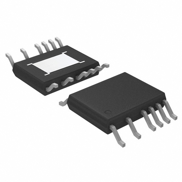


 工商网监
湘ICP备2023018690号
工商网监
湘ICP备2023018690号

