LT8603
42V, Low IQ, Quad Output Triple Monolithic
Buck Converter and Boost Controller
FEATURES
DESCRIPTION
Flexible Power Supply System Capable of Four
Regulated Outputs with VBATT 3.1V for INTVCC or > 4.6V
for INTVCC4 the internal regulators will draw their power
from BIAS. This will reduce the on-chip power dissipation
during full frequency operation and reduce the effective
no-load sleep current at the input.
PG4 (Pin 11): Power Good Indicator Channel 4. This pin
is an open-drain output that pulls low until the Channel
4 feedback voltage is greater than 92% of its reference
voltage.
FSEL4A, FSEL4B (Pins 12, 17): Boost Converter
Frequency Select and RUN Control. These pins are logic
inputs. When both pins are low, the boost controller is
shut down. The boost controller switching frequency is
controlled using these pins according to Table 2 in the
Applications Information section.
GATE4 (Pin 15): External MOSFET Gate Drive Output.
This pin switches from GND to VINTVCC4 to turn on the
low side power MOSFET in the BOOST converter. See
the Applications Information section for information on
MOSFET selection.
INTVCC4 (Pin 16): Internal Boost Regulator Output. Do
not load the INTVCC4 pin with external circuitry. INTVCC4
is 4.6V when BIAS < 4.6V, 5V when BIAS > 5V, and equal
to BIAS when BIAS is between 4.6V and 5V. Decouple to
ground with a low ESR 4.7µF capacitor.
ISP4, ISN4 (Pins 19, 18): Boost Controller Current Sense
Inputs. Connect a current sense resistor of appropriate
value between these pins with ISP4 connected to the
input supply and ISN4 to the application inductor. See
the Applications Information section for sense resistor
selection details.
TRKSS1, TRKSS2 (Pins 21, 20): Track/Soft-Start Inputs
for the High Voltage Converters. When this pin is below
1V, the converter regulates the FB pin to the TRKSS voltage instead of the internal reference. The TRKSS pin has a
2.4μA pull-up current. Connect a capacitor between either
of these pins to ground to program a soft-start time for
the associated channel.
EN/UVLO (Pin 22): Enable/Undervoltage Lockout Input.
The LT8603 is in low power shutdown when this pin is
below 0.4V. Between 0.4V and 1.1V, the part will turn on
the internal reference. A precision threshold at 1.2V (rising) enables the switching regulators. The precision
threshold allows the EN/UVLO pin to be used as an input
undervoltage lockout by connecting to resistor divider
between VIN and GND. When the EN/UVLO voltage is
between 0.4V and 1.2V, the LT8603 input current will
depend on the mode selected, the VIN voltage and EN/
UVLO voltage.
VIN (Pin 23): Power Supply to Internal Functions. This
pin provides power to the LT8603 internal circuitry. This
pin must reach 4V for the boost converter to complete its
internal soft-start delay of 1ms.
FB4 (Pin 24): Feedback Input Pin for the Boost Converter.
The converter regulates FB4 to 0.8V.
FB1, FB2 (Pins 26, 25): Feedback Input Pins for the
High Voltage Converters. The converters regulate the
Rev. B
For more information www.analog.com
11
�LT8603
PIN FUNCTIONS
corresponding feedback pin to the lesser of 1V or the
voltage on the associated TRKSS pin.
FB3 (Pin 27): Feedback Input Pin for the Low Voltage
Converter. The converter regulates FB3 to 0.8V.
INTVCC (Pin 28): Internal Regulator Bypass. Do not load
the INTVCC pin with external circuitry. INTVCC is 3.1V
when BIAS < 3.1V, 3.4V when BIAS > 3.4V, and equal to
BIAS when BIAS is between 3.1V and 3.4V. Decouple to
ground with a low ESR 4.7µF capacitor.
RT (Pin 29): Frequency Programming Resistor. Connect
a resistor between this pin and ground to set the internal
oscillator frequency. This pin should not be left open.
RUN3 (Pin 30): Enable Input For Low Voltage Channel 3.
Channel 3 is enabled when the voltage on this pin exceeds
1.2V. The RUN3 pin has a precise threshold so it can be
used to create a UVLO function or be sequenced from
another channel. There is an internal soft-start timer
which ramps the output up in approximately 1ms.
CPOR (Pin 31): Power-On Reset Timing Capacitor.
A capacitor from this pin to ground sets the period of
the power-on reset oscillator timer. See the Applications
Information Section for details.
RST (Pin 32): Active Low Reset Output. This pin is the
output of the power-on reset function. This pin is an opendrain output with a weak pull-up to approximately 2V. This
pin is held low until the power on reset timer times out.
12
SYNC (Pin 33): Clock Synchronization and Mode Select
Input. This pin allows the LT8603 to synchronize its
switching frequency to an external clock. When an external
clock is applied, the LT8603 will operate in pulse-skipping
mode. If clock synchronization is not used, connect this
pin to ground to enable low ripple Burst Mode operation
or connect high to enable pulse-skipping operation.
PVIN3 (Pin 34): Input Supply Voltage to Low Voltage
Channel 3. This pin will normally be connected to the
output of one of the high voltage converters but can be
supplied from any voltage in the specified range. It should
be bypassed locally with a low ESR ceramic capacitor to ground with a low inductance connection to the
exposed pad.
SW3 (Pin 36): Low Voltage Converter Switch Node. This
is the output of the internal power switches for Channel 3.
PVIN1, PVIN2 (Pins 37, 14): Input Supply to High Voltage
Channels 1 and 2, respectively. These pins can be powered from the boost converter output or any voltage in
the specified range. Each pin should be bypassed locally
with a low ESR ceramic capacitor to ground with a low
inductance connection to the exposed pad.
POREN (Pin 39): Power-On Reset Enable. This is a logic
input that starts the ramp on the POR timing capacitor.
This input has a weak pull-up to allow direct connection
to open-drain outputs.
Rev. B
For more information www.analog.com
�LT8603
BLOCK DIAGRAM
EN/UVLO
VIN
RT
BIAS
CLK1
OSCILLATOR
SYNC
FSEL4A
FSEL4B
BOOST DIVIDER
AND SLOPE GEN
CLK2
INTVCC
INTVCC
CLK4
SLOPE4
5V
INTVCC4
REGULATOR
REFERENCE
INTVCC4
INTVCC4
POREN
0.8V
POWER-ON
RESET
CPOR
3.4V
INTVCC
REGULATOR
STANDBY/BIAS
1V
RST
BST1
BST2
ILIM1
PVIN1
–
+
CLK1
CURRENT
SENSE
COMPARATOR
LOGIC 1
SW2
LOGIC 2
DRIVER
REVERSE
CURRENT
COMPARATOR
–
+
DRIVER
REVERSE
CURRENT
COMPARATOR
ERROR
AMPLIFIER
FB1
–
+
+
2.4µA
–
+
LOOP
COMPENSATION
ILIM2
ILIM1
1.08V
–
+
–
+
ILIM3
PVIN3
–
+
CLK1
2.4µA
PG2
INTVCC4
GATE4
LOGIC 4
DRIVER
DRIVER
REVERSE
CURRENT
COMPARATOR
–
+
CURRENT
COMPARATOR
–
+
ERROR
AMPLIFIER
–
+
+
SS3
1.08V
CLK4
LOGIC 3
FB3
TRKSS2
0.92V
CURRENT
SENSE
COMPARATOR
SW3
GND
FB2
–
+
+
LOOP
COMPENSATION
1V
0.92V
PG1
GND
ERROR
AMPLIFIER
1V
TRKSS1
PVIN2
–
+
CURRENT
SENSE
COMPARATOR
SW1
GND
ILIM2
CLK2
LOOP
COMPENSATION
+
–
ITRIP
1.2V
ILIM4
–
+
+
LOOP
COMPENSATION
ILIM3
0.8V
0.736V
0.864V
ISP4
ISN4
ERROR
AMPLIFIER
FB4
SS4
0.8V
–
+
PG3
GND
RUN3
PG4
–
+
0.736V
8603 BD
Rev. B
For more information www.analog.com
13
�LT8603
OPERATION
The LT8603 combines two 42V input step-down converters (Channels 1 and 2), one 5.5V input step-down converter (Channel 3) and a boost controller (Channel 4) to
provide a flexible system that can be configured to generate up to four regulated outputs. For example, the boost
controller may be used to guarantee a supply to the high
voltage converters above their minimum dropout voltage
even during the cold crank cycle in an automobile.
Start-Up
When enabled by setting the EN/UVLO voltage above its
threshold, the LT8603 INTVCC regulator charges its output
capacitor to supply the internal chip circuitry. If BIAS is
higher than 3.1V, BIAS supplies current to the INTVCC
regulator to reduce VIN quiescent current.
The boost controller is enabled with a logic high on
either one or both of the FSEL4A and FSEL4B pins. Once
enabled, the INTVCC4 regulator charges its output capacitor bringing the INTVCC4 supply into regulation. When
the voltage at INTVCC4 exceeds 4.0V, the boost controller
gate driver will begin supplying gate drive pules to the
external MOSFET. Like the INTVCC regulator, the INTVCC4
regulator can also draw power from the BIAS pin when
BIAS exceeds 4.6V.
the next clock cycle will be delayed until switch current
returns to a safe level. The TRKSS pins can be used for
controlled start-up or tracking of another supply.
Low Voltage Buck Regulator (Channel 3)
The low voltage channel is a synchronous buck regulator
that operates from an independent PVIN pin. The PVIN pin
has an undervoltage lockout set at 2.35V. The top power
MOSFET is turned on at the beginning of each oscillator
cycle, and turned off when the current flowing through
the top MOSFET reaches a level determined by the error
amplifier. The error amplifier measures the output voltage
through an external resistor divider tied to the FB3 pin to
control the peak current in the top switch. The reference of
the error amplifier is an internal 800mV reference. While
the top MOSFET is off, the bottom MOSFET is turned on
for the remainder of the oscillator cycle or until the inductor current starts to reverse. If overload conditions result
in more than 2.4A flowing through the bottom switch,
the next clock cycle will be delayed until switch current
returns to a safe level.
The low voltage channel has a RUN3 pin to allow power
sequencing, plus an internal soft-start circuit that ramps
the output voltage up in 1ms.
High Voltage Buck Regulators (Channels 1 and 2)
Boost Controller (Channel 4)
Each high voltage channel is a synchronous buck regulator that operates from an independent PVIN pin. The
internal top power MOSFET is turned on at the beginning
of each oscillator cycle, and turned off when the current
flowing through the top MOSFET reaches a level determined by the error amplifier. The error amplifier measures
the output voltage through an external resistor divider
tied to the FB pin to control the peak current in the top
switch. The reference of the error amplifier is determined
by the lower of the internal 1V reference and the voltage
at its TRKSS pin. While the top MOSFET is off, the bottom
MOSFET is turned on for the remainder of the oscillator
cycle or until the inductor current starts to reverse. If
overload conditions result in more than 2A for Channel 1
or 3.3A for Channel 2 flowing through the bottom switch,
The boost controller includes an error amplifier, loop
compensation, current comparator, switch control logic,
and a gate driver. The controller is enabled and its clock
frequency selected by control of the FSEL4A and FSEL4B
pins as described in the Applications Information section.
14
The required external N-channel MOSFET is turned on
by the internal clock and turned off when the inductor
current sensed by the current comparator exceeds its
threshold. The error amplifier adjusts the current comparator threshold by comparing the FB4 voltage to an
internal 0.8V reference voltage. The output voltage is set
by a resistor divider from the output to the FB4 pin. The
internal INTVCC4 regulator provides the gate drive for the
external MOSFET.
Rev. B
For more information www.analog.com
�LT8603
OPERATION
Multiphase Switching
Power Good Comparators
The oscillator generates two clock signals 180° out of
phase with each other. Channels 1 and 3 operate from
CLK1, while Channels 2 and 4 operate from CLK2. The
clock for Channel 4 may be selected as either a ÷1,
÷2 or ÷5 version of CLK2 using the FSEL4A and FSEL4B
pins. Regardless of the divide ratio chosen, the Channel 4
clock edges remain aligned to the CLK2 edges.
Channels 1, 2 and 3 have power good comparators that
trip when the feedback pin is more than 8% above or
below its reference voltage. Channel 4 has a power good
comparator that indicates when the output voltage is more
than 8% below its reference. The PG output pins are opendrain and pulled low when the corresponding output is out
of regulation. The PG outputs are not valid until INTVCC
rises to 2.7V.
Since a buck regulator only draws input current during the
top switch on cycle, multiphase operation reduces peak
input current and doubles the input current frequency.
These effects reduce input current ripple and reduce the
input capacitance required.
Undervoltage Lockout
The EN/UVLO pin is used to put the LT8603 in shutdown,
reducing the input current to less than 1μA. The accurate
1.2V threshold of the EN/UVLO pin provides a programmable VIN undervoltage lockout through an external resistor divider tied to the EN/UVLO pin. A 50mV hysteresis
voltage on the EN/UVLO pin prevents switching noise
from inadvertently shutting down the LT8603.
Power-On Reset Timer
The LT8603 includes a power-on reset timer. The
power-on reset timeout period is adjustable using an
external capacitor on the CPOR pin as described in the
Applications Information section. The timer is initiated
when the POREN pin is higher than 1.2V. The output of
the POR timer, the RST pin, is an open-drain output with
a weak internal pull-up of 100k to approximately 2V. RST
is held low until the expiration of the POR timer. The RST
pin is only valid when the LT8603 is enabled and INTVCC
is above 2.7V.
Rev. B
For more information www.analog.com
15
�LT8603
APPLICATIONS INFORMATION
SYSTEM ARCHITECTURE
Switching Frequency
The LT8603 combines three buck converters with a boost
controller to provide a flexible system supply that can
be configured to generate up to four regulated outputs.
The 4 channels are independently powered and can be
connected in a variety of ways. For example, the output
of the boost may be used to supply the input voltage to
the buck converters resulting in three tightly regulated
outputs even when the boost input voltage falls below
the regulated buck outputs such as occurs during an
automotive cold crank scenario. Alternatively, if the boost
controller is driven from a buck output or is configured as
a SEPIC converter, the LT8603 provides up to four tightly
regulated outputs.
All 4 channels share a single oscillator. The buck channels switch at the oscillator frequency. The boost channel can switch at fOSC, fOSC/2 or fOSC/5. The switching
frequency range of all 4 channels should be determined
before selecting the oscillator frequency. A low frequency
usually provides better efficiency and a wider operating
range due to lower switching losses and less sensitivity
to timing constraints such as minimum on- and off-times.
A high switching frequency uses smaller components and
moves the switching noise away from sensitive frequency
bands, such as the AM radio band, but does so at the
cost of lower efficiency. A high switching frequency also
decreases the duty cycle range because of finite minimum on- and off-times which are independent of the
switching frequency.
VIN Voltage Range
The minimum voltage at VIN for the LT8603 internal circuitry and the buck converters to start is 3.1V, however,
at least 4V is required for the boost controller and the
INTVCC4 regulator to start. The boost controller can be
configured to supply VIN and the PVIN pins once it has
started; after start-up the input voltage to the boost controller can go lower than 3V.
The oscillator frequency can be programmed from 250kHz
to 2.2MHz by tying a resistor from the RT pin to ground.
Table 1 shows the necessary value of RT for some common switching frequencies.
Table 1. Oscillator Frequency (fOSC) vs RT Value
OSCILLATOR
FREQUENCY (MHz)
RT (kΩ)
0.25
244
0.35
173
Enable and Undervoltage Lockout
The EN/UVLO pin can be used to to program a minimum
system start voltage or an undervoltage lockout (UVLO)
voltage. It has an internal threshold of 1.2V with 50mV
hysteresis. The UVLO divider circuit is shown in Figure 1.
The UVLO threshold is given by:
V(UVLO ) =
R UV1 + R UV 2
R UV 2
• 1.2V
RUV1
LT8603
EN/UVLO
RUV2
120
79.2
1.0
58.9
1.25
46.8
1.5
38.7
1.75
33.0
2.0
28.7
2.2
26.0
The following equation approximates the values shown
in Table 1:
VIN
VIN OR VBATT
0.5
0.75
8603 F01
RT =
59.8
(fOSC – 0.007)
– 1.3
The RT pin is sensitive to noise so the resistor should be
placed close to the LT8603 and away from noise sources.
Figure 1. UVLO Divider
16
Rev. B
For more information www.analog.com
�LT8603
APPLICATIONS INFORMATION
The internal oscillator of the LT8603 can be synchronized
to an external clock of 250kHz up to 2.2MHz applied to
the SYNC pin. The RT value should be chosen such that
the frequency set by RT is close to the anticipated external
clock frequency.
Mode Selection and Synchronization
To select low ripple Burst Mode operation, the SYNC
pin should be connected to a voltage below 0.3V such
as ground. To select pulse-skipping operation, connect
the SYNC pin to an available voltage above 1.2V such
as INTVCC.
To synchronize the LT8603 to an external frequency, drive
the SYNC pin with a pulse train with a high voltage above
1.2V and a low voltage below 0.3V. The minimum pulse
width is 120ns for a high pulse and 90ns for a low pulse.
The LT8603 will operate in pulse-skipping mode while
synchronized to an external clock. The LT8603 may be
synchronized over a 250kHz to 2.2MHz range. The RT
resistor should be chosen to set the LT8603 switching
frequency close to the synchronization input.
For some applications it is desirable for the LT8603 to
operate in pulse-skipping mode, offering two major differences from Burst Mode operation. First, in pulse-skipping
mode the clock stays awake at all times and all switching
cycles are aligned to the clock. Second, full frequency
switching is reached at a lower output load in pulse-skipping than Burst Mode operation. These two differences
come at the expense of increased quiescent current for
pulse-skipping. To enable pulse-skipping mode, the SYNC
pin is tied high either to a logic output or to the INTVCC
pin. Do not leave the SYNC pin floating.
pin is connected to a switching regulator channel it will
improve efficiency, reduce on-chip dissipation and lower
the sleep current. The INTVCC may be used to configure
other inputs and supply pull-ups related to the LT8603. It
is not recommended to draw more than 1mA or connect
INTVCC to any components not related to the LT8603 to
avoid unexpected interactions.
BOOST CONTROLLER
Functional Description
Channel 4 is a set of functional elements that are connected to external components to form a boost converter.
The Block Diagram in Figure 2 shows these elements and
how they are connected internally.
The error amplifier compares a fractional part of the output voltage to an 800mV reference. The output, ILIM4,
goes to the current comparator to set the peak current.
The current comparator senses the inductor current using
a small sense resistor across the ISP4 and ISN4 pins. The
trip level is set by the error amplifier output, ILIM4, and
the slope compensation signal, SLOPE4. The maximum
CLK2
BIAS
VIN
FSEL4A
FSEL4B
BOOST DIVIDER
AND SLOPE GEN
CLK4
GATE4
LOGIC 4
DRIVER
CURRENT
COMPARATOR
INTVCC Regulator
ISP4
+
–
ITRIP
SLOPE4
The INTVCC supplies the common circuitry such as the
oscillator and reference but its main current demand
comes from the gate drivers for the high voltage buck
converters. The current draw will depend on the operating frequency, the higher the switching frequency, the
greater the current drawn from INTVCC. The regulator is
supplied by VIN at start-up, but it will draw its supply
current from BIAS if BIAS is at least 3.1V. If the BIAS
5V INTVCC4
INTVCC4
REGULATOR
ISN4
ILIM4
–
+
+
LOOP
COMPENSATION
ERROR
AMPLIFIER
FB4
SS4
0.8V
PG4
–
+
0.736V
8603 F02
Figure 2. Boost Controller Block Diagram
Rev. B
For more information www.analog.com
17
�LT8603
APPLICATIONS INFORMATION
trip level is 50mV. ISP4 and ISN4 have an operational
common range of 2V to 42V and an absolute maximum
rating of ±42V. This allows reverse battery protection with
a single diode in series with external MOSFET drain.
The logic block turns on the external MOSFET on a CLK4
signal, and then turns it off on an ITRIP from the current
comparator, or when maximum duty cycle is reached.
The LT8603 has a frequency divider that allows the controller switching frequency to be less than the oscillator frequency. The boost controller is specified for a fSW
between 250kHz and 2.2MHz; do not set the divider to
operate the boost controller below 250kHz. The FSEL4A
and FSEL4B pins control the oscillator frequency as
shown in Table 2.
5V, the regulator generates 5V and draws power from
BIAS. Do not use the INTVCC4 output for external circuitry.
A comparator senses when the output voltage is above
92% of the programmed value and generates a power
good signal at the PG4 pin.
Setting the Output Voltage
The boost controller’s output voltage is set by connecting
the FB4 pin to a resistor divider from the output as shown
in Figure 3.
VOUT4
LT8603
R1
FB4
R2
Table 2. Boost Frequency Selection
BOOST FREQ fSW4
FSEL4A
FSEL4B
0 (Boost Shutdown)
Low
Low
fOSC/5
High
Low
fOSC/2
Low
High
fOSC
High
High
The boost controller is enabled by the FSEL4A and FSEL4B
pins. When both pins are low, the boost controller is shut
down. When either or both pins are set high, a boost
controller start-up sequence is initiated. During start-up,
the INTVCC4 regulator is turned on charging the external
INTVCC4 capacitor. Once INTVCC4 reaches 4V, the controller logic is turned on and switching begins. A 1ms softstart ramp is applied to the error amplifier to minimize
inrush current.
The INTVCC4 regulator is a low dropout, linear regulator
that provides power to the GATE4 drive circuit. It is dedicated to the boost controller and is shut down when the
boost controller is shut down. It can draw power from
either VIN or BIAS, depending on the BIAS voltage. When
BIAS is less that 4.6V, the regulator will draw power from
VIN and regulate to 4.6V. When BIAS is greater than 4.6V
but less than 5V, the regulator sets INTVCC4 equal to BIAS
and draws power from BIAS. When BIAS is greater than
18
8603 F03
Figure 3. Feedback Resistor Divider
The value of R2 is best selected first as this establishes
how much current is in the string based on I = VFB4/R2
where VFB4 = 0.8V. The current should be chosen such
that it is not influenced by anticipated leakage or noise.
R1 can then be calculated from:
R1 = R2 • ((VOUT4/VFB4) – 1)
Boost Configuration
The LT8603 boost controller configured as a standard
boost regulator is shown in Figure 4. The boost controller output voltage is set by connecting FB4 to an external
divider. For the following example, R2 and R3 are chosen
such that OUT4 = 8V. If the battery voltage (VBATT) is
above 8V plus a diode forward voltage, the boost controller will be inactive consuming minimal quiescent current.
If the battery voltage drops below 8V plus a diode forward
voltage, such as during an automotive cold crank cycle,
the boost controller will become active to maintain 8V
at OUT4. With OUT4 connected to VIN, the input supply
must reach 4V plus the diode forward voltage to start.
Rev. B
For more information www.analog.com
�LT8603
APPLICATIONS INFORMATION
SD1
L1
R1
VBATT
(R2+R3)
when VBATT < VOUT 4 + VF(SD1)
R3
= VBATT – VF(SD1) = when VBATT ≥ VOUT 4 + VF(SD1)
VOUT 4 = 0.8 •
SD2*
C2
ISP4
ISN4
EN/UVLO
INTVCC
LT8603
INTVCC4
C3
VIN
R2
GATE4
M1
FB4
RT FSEL4A FSEL4B GND
C1
R3
INTVCC4
8603 F04
*SD2 IS FOR REVERSE INPUT PROTECTION. SHORT IF NOT NEEDED.
Figure 4. Channel 4 in Boost Configuration
Once started however, the LT8603 will maintain the output
voltage at OUT4 with VBATT as low as 2V. The ISP4 and
ISN4 pins sense the inductor current for the current mode
control loop across current sense resistor R1. The ISP4
and ISN4 pins will accurately sense the inductor current
down to 2V and will tolerate negative voltages as large as
–42V without damage.
By adding diode SD2 in series with the main switch transistor M1, the entire regulator will be tolerant of negative
input supply voltages.
One of the limitations of the boost configuration is that
it cannot provide short-circuit protection for the boost
output as the diode always provides a DC current path
from input to output. If short-circuit overload protection
is required the SEPIC configuration should be considered.
See the SEPIC Configuration section for more information
on the SEPIC converter.
Boost: Duty Cycle and Max Switching Frequency
In continuous conduction mode (CCM), the operating
duty cycle as a function of input and output voltage is
given by:
⎞
⎛ V +V –V
D = ⎜ OUT D BATT ⎟
V +V
⎠
⎝
OUT
Thus the maximum duty cycle (DMAX) in terms of the
minimum VBATT is:
DMAX =
VOUT + VD – VBATT (MIN )
VOUT + VD
For a given input and output voltage, the switching frequency is limited by the expected maximum duty cycle,
DMAX, and minimum switch off time, tOFF(MIN). The
fSW(MAX) at DMAX is given by:
fSW(MAX) =
DMAX
t OFF(MIN)
Boost: Inductor and Sense Resistor Selection
The boost regulator inductor and sense resistor (RSENSE)
should be sized according to the maximum input current. The maximum input current will occur at the minimum input voltage (maximum duty cycle) and maximum
output load.
The maximum average inductor current, which is equal to
the average input current, can be calculated from:
IL(MAX ) =
IOUT(MAX )
1 – DMAX
D
where VD is the forward voltage drop of the diode.
Rev. B
For more information www.analog.com
19
�LT8603
APPLICATIONS INFORMATION
From this the ripple current can be specified using:
∆IL = χ •IL(MAX) = χ •IOUT(MAX) •
1
1 – DMAX
where χ in the above equation represents the percentage peak-to-peak ripple current in the inductor relative to
IL(MAX). Choosing the inductor ripple current, ∆IL, has a
direct impact on the choice of the inductor value and the
converter’s maximum output current capability. Choosing
smaller values of ∆IL increases the converter’s output current capability but requires larger inductors. Choosing
larger values of ∆IL provides faster transient response
and allows the use of smaller inductors but results in
higher input current ripple, greater core losses, and lower
output current capability. In addition, larger values of ∆IL
at high duty cycle may result in sub-harmonic oscillation.
The typical range for χ is 20% to 40% though careful
evaluation of system stability should be made to ensure
adequate design margin. The peak inductor current will be
the average inductor current plus half the ripple current.
The LT8603 current sense comparator has a built-in current limit threshold of 50mV across ISP4 and ISN4 so the
peak voltage across the sense resistor should be kept to
no more than 80% of this or 40mV. Therefore, the value
of RSENSE should be:
R SENSE =
0.04
IL(PEAK )
The inductor value to achieve the required ripple is given
by following equation:
VBATT (MIN )
∆IL • fSW
• DMAX
The inductor should have a saturation current exceeding
the current limit value of:
ILIM =
20
R SENSE
For example, a 4mΩ could dissipate up to 0.625W.
Boost: MOSFET Selection
For the boost configuration, the selected external MOSFET
should have a BVDSS rating exceeding, with margin, the
larger of either the maximum input voltage or the boost
output voltage plus a diode forward voltage. The maximum input voltage should include careful consideration
of possible transient conditions. In addition, the chosen
MOSFET should be compatible with the LT8603’s nominal gate drive of 4.6V and have a low value of RDS(ON)
for best efficiency. The current rating for the MOSFET
must be greater than the peak inductor current. Finally,
the maximum gate drive current required by the external
MOSFET should not exceed the 40mA capability of the
LT8603. The current drawn by the gate driver is given by:
IDRIVE = Q g • fsw
For example, if Qg is 20nC and fSW is 1MHz, the drive
requirement is 20mA.
⎛ χ ⎞ IOUT(MAX)
IL(PEAK) = ⎜ 1+ ⎟ •
⎝ 2 ⎠ 1 – DMAX
L=
0.05 2
P
=
RSENSE
where Qg is the MOSFET gate charge and fSW is programmed switching frequency.
IL(PEAK) can be calculated from:
Finally, the ESR and magnetic loss of the inductor contribute to overall system power loss. For best efficiency,
an inductor with low ESR and a core rated for the desired
operating frequency should be chosen. The sense resistor should be chosen to have adequate power handling
capability. The maximum power dissipation is given by:
Boost: Diode Selection
In the boost converter, the rectifier diode, SD1, only conducts when the switch is off. The average diode current
is equal to the output current. The peak current is equal
to the peak inductor current and is given by:
⎛ χ ⎞ IOUT(MAX )
ID(PEAK ) = ⎜ 1+ ⎟ •
⎝ 2 ⎠ 1 – DMAX
0.05
R SENSE
Rev. B
For more information www.analog.com
�LT8603
APPLICATIONS INFORMATION
The power dissipated by the diode is given by:
L
PD = IOUT (MAX ) • VD
VBATT
D
SW
Therefore, a rectifier diode should be chosen with a low
forward voltage drop at peak current for best efficiency
and a reverse breakdown voltage greater than VOUT4(MAX).
VOUT
COUT
RL
5a. Circuit Diagram
If the reverse protection diode (SD2) is needed, the
reverse breakdown voltage must be greater than the
desired reverse polarity protection.
IIN
IL
5b. Inductor and Input Currents
Boost: Output Capacitor
The output capacitor has two essential functions. First, the
output capacitor filters the LT8603’s discontinuous output
current to produce the DC output current. In this role, the
capacitor determines the output ripple, thus low impedance at the switching frequency is important. Second, the
output capacitor stores energy in order to satisfy transient
load conditions and stabilize the LT8603’s control loop.
Typically, the low equivalent series resistance of X5R and
X7R ceramic capacitors provide low output ripple and
good transient response.
ISW
tON
5c. Switch Current
ID
IO
5d. Diode and Output Currents
For some applications, transient performance can be
improved with higher output capacitance and/or the
addition of a feedforward capacitor placed between the
boost output voltage and the boost feedback pin. Note that
larger output capacitance may be required when lower
switching frequencies are used or when there is significant inductance to the load due to long wire or cables.
Increasing the output capacitance will also decrease the
output ripple.
When choosing a capacitor, special attention should be
given to the capacitor’s data sheet to understand the
effective capacitance under the relevant operating conditions of voltage bias and temperature. For good starting
values, refer to the Typical Applications section. For all
applications, careful evaluation of system stability should
be made to ensure adequate design margin.
tOFF
VOUT
(AC)
ΔVCOUT
ΔVESR
RINGING DUE TO
TOTAL INDUCTANCE
(BOARD + CAP)
5e. Output Voltage Ripple Waveform
8603 F05
Figure 5. Switching Waveforms for a Boost Converter
Boost: Input Capacitor
The input capacitor is in series with the inductor so the
input current waveform is continuous and the di/dt is
limited.
An input capacitor should be chosen to handle the RMS
input capacitor ripple current as given by:
IRMS(CIN) = 0.6 • χ • IOUTMAX
Rev. B
For more information www.analog.com
21
�LT8603
APPLICATIONS INFORMATION
Ensure that capacitors present at the input are rated to
withstand any voltage transients that may be applied.
The value of input capacitance is a function of the source
impedance. In general, the higher the source impedance,
the higher the required input capacitance. The Typical
Applications section provides reasonable starting values
for input capacitance but careful evaluation of each application must be made to ensure adequate design margin.
SEPIC Configuration
Figure 6 shows the boost controller configured as a single-ended primary inductance converter or SEPIC. The
SEPIC configuration offers two primary advantages over
the standard boost configuration. First, it operates like a
buck/boost which means it will regulate to an accurate
output voltage for any input voltage. Second, it offers
short-circuit protection and 0V output in shutdown since
there is no DC path from the input to the output. The disadvantage is a more complex circuit requiring additional
components as compared to a standard boost configuration. Since there is no DC path to the output, the LT8603
VIN cannot be connected directly to the SEPIC output. As
a result, diode SD3 is used to ensure start-up, and SD4
is used to ensure operation to low VBATT once started. If
R1
VBATT
VBATT drops below 4V after the SEPIC is in regulation,
SD4 maintains VIN at the SEPIC output voltage. Just as
with the standard boost configuration, optional diode SD2
provides reverse battery protection.
Figure 7 shows a simplified topology and the current
flow for each of the switch positions once steady state
is reached. Both inductors increase current during the
switch on cycle (Figure 7b). The DC currents of L1 and
L2 are not necessarily equal: IL1(DC) must be equal to
IVBATT(DC) since there is no other DC path for the current
flow from VBATT. By the same argument, IL2(DC) must be
equal to IOUT(DC). Figure 8 shows the current waveforms
of the SEPIC converter.
Although uncoupled inductors can be used in the SEPIC
converter, coupled inductors provide several advantages
and are preferred for most applications. Uncoupled inductors require double the inductance of the coupled inductors and two inductors at twice the inductance usually
cost more than one coupled inductor. Also, uncoupled
inductors form a tank with the coupling capacitor which
can ring at very low frequencies. Uncoupled inductors
can be an advantage, however, in high power or high
duty cycle converters since the current is split between
two cores.
C5
L1
•
SD3
SD1
VOUT 4 = 0.8 •
(R2+R3)
R3
SD2*
SD4
5V
BIAS
C1
C2
ISP4
ISN4 VIN
EN/UVLO
INTVCC
LT8603
R2
M1
FB4
INTVCC4
RT FSEL4A FSEL4B GND
C4
R3
L2
INTVCC4
•
C3
GATE4
8603 F06
*SD2 IS FOR REVERSE INPUT PROTECTION. SHORT IF NOT NEEDED.
Figure 6. Channel 4 in SEPIC Configuration
22
Rev. B
For more information www.analog.com
�LT8603
APPLICATIONS INFORMATION
C1
L1
D1
VBATT
SW
L2
The lower of these frequencies is the maximum switching
frequency for the SEPIC converter.
VOUT
+
+
•
COUT
+
RL
•
7a. SEPIC Topology
•
VOUT
+
+
VIN
L1
VBATT
+
L2
RL
•
7b. Current Flow During Switch On-Time
VIN
L1
VBATT
D1
+
+
•
VOUT
+
L2
RL
•
SEPIC: Inductor and RSENSE Selection
Choosing the inductor ripple current, ∆IL, has a direct
impact on the choice of the inductor value and the converter’s maximum output current capability. Choosing
smaller values of ∆IL increases the converter’s output
current capability but requires larger inductors. Choosing
larger values of ∆IL provides faster transient response and
allows the use of smaller inductors but results in higher
input current ripple, greater core losses, and lower output
current capability. In addition, larger values of ∆IL at high
duty cycle may result in sub-harmonic oscillation.
Given an operating input voltage range and operating frequency, the inductor value is given by:
7c. Current Flow During Switch Off-Time
8603 F07
Figure 7. SEPIC Topology and Current Flow
⎞
⎛
VOUT + VD
D= ⎜
⎝ VBATT + VOUT + VD ⎟⎠
The maximum switching frequency of the SEPIC converter is limited by both maximum and minimum duty
cycles. The maximum duty cycle is set by VBATT(MIN). The
maximum switching frequency, fSW(MAX) at VBATT(MIN) is
given by:
fSW(MAX)@VBATT(MIN) = 1 –
VOUT + VD
⎡
⎤
⎢V
⎥
+
V
+
V
D⎦
OUT
⎣ BATT(MIN)
t OFF(MIN)
The minimum duty cycle is set by VBATT(MAX). The maximum switching frequency at VBATT(MAX) is given by:
fSW(MAX)@VBATT(MAX)
VOUT + VD
⎡
⎤
⎢V
⎥
+
V
+
V
BATT(MAX)
D⎦
OUT
= ⎣
t ON(MIN)
VBATT(MIN) • DMAX
ΔIL • fSW
where,
SEPIC: Duty Cycle and Frequency
With the SEPIC configuration operating in continuous
conduction mode (CCM), the duty cycle is given by:
L=
ΔIL =
χ •IOUT(MAX) • DMAX
1– DMAX
χ in the above equation represents the percentage peakto-peak ripple current in the inductor relative to the maximum average inductor current. The typical range of χ is
20% to 40% though careful evaluation of system stability
should be made to ensure adequate design margin.
For coupled inductors, L1 = L2 and the effective inductance is doubled due to the mutual inductance. The value
of each equal winding is given by:
L1 = L2 =
VBATT(MIN) • DMAX
2 • ΔIL • fSW
The maximum input current of the SEPIC converter is calculated at the minimum input voltage and full load current.
The peak inductor current can be significantly higher than
the output current. The following equations assume CCM
operation and calculate the maximum peak inductor current at minimum VBATT:
Rev. B
For more information www.analog.com
23
�LT8603
APPLICATIONS INFORMATION
For a coupled inductor:
IL1
⎛ V +V ⎞
⎛ χ⎞
IL(PEAK) = ⎜ 1+ ⎟ •IOUT(MAX) • ⎜ 1+ OUT D ⎟
⎝ 2⎠
⎝ VBATT(MIN) ⎠
IIN
SW
ON
SW
OFF
8a. Input Inductor Current
For uncoupled inductors:
IO
IL2
V + VD
⎛ χ⎞
IL1(PEAK) = ⎜ 1+ ⎟ •IOUTMAX • OUT
⎝ 2⎠
VBATT(MIN)
VBATT(MIN) + VD
⎛ χ⎞
IL2(PEAK) = ⎜ 1+ ⎟ •IOUT(MAX) •
⎝ 2⎠
VBATT(MIN)
8b. Output Inductor Current
IIN
IC1
RSENSE can then be calculated by:
R SENSE =
IO
8c. DC Coupling Capacitor Current
0.04
IL1(PEAK )
The chosen inductor(s) should be rated for the maximum
expected current.
ID1
IO
SEPIC: MOSFET Selection
8d. Diode Current
For the SEPIC configuration, the selected MOSFET should
have a BVDSS rating exceeding, with margin, the maximum input voltage plus the maximum output voltage plus
the maximum diode forward voltage. The maximum input
voltage should include careful consideration of possible
transient conditions. In addition, the chosen MOSFET
should be compatible with the LT8603’s nominal gate
drive of 4.6V and have a low value of RDS(ON) for best
efficiency. The current rating for the MOSFET must be
greater than the peak switch current of:
ISW(PEAK)
1
⎛ χ⎞
= ⎜ 1+ ⎟ •IOUT(MAX) •
⎝ 2⎠
1– DMAX
VOUT
(AC)
ΔVCOUT
ΔVESR
RINGING DUE TO
TOTAL INDUCTANCE
(BOARD + CAP)
8e. Output Ripple Voltage
8603 F08
Figure 8. SEPIC Converter Switching Waveforms
SEPIC: Diode Selection
Finally, the maximum gate drive current required by the
external MOSFET should not exceed the 40mA capability
of the LT8603. The current drawn by the gate driver is
given by:
For the rectifier diode, SD1, the peak reverse voltage that
the diode must withstand is:
IDRIVE = Q g • fSW
The average forward current is equal to the output current
and the peak current is given by:
VBATT(MAX ) + VOUT
24
⎞
⎛ V +V
⎛ χ⎞
ID(PEAK) = ⎜ 1+ ⎟ •IOUT(MAX) • ⎜ OUT D +1⎟
⎝ 2⎠
⎝ VBATT(MIN) ⎠
Rev. B
For more information www.analog.com
�LT8603
APPLICATIONS INFORMATION
The power dissipated by the diode is:
SEPIC: Output Capacitor
PD = IOUT(MAX ) • VD
The output capacitor has two essential functions. First, the
output capacitor filters the LT8603’s discontinuous output
current to produce the DC output current. In this role, the
capacitor determines the output ripple, thus low impedance at the switching frequency is important. Second, the
output capacitor stores energy in order to satisfy transient
load conditions and stabilize the LT8603’s control loop.
Typically, the low equivalent series resistance of X5R and
X7R ceramic capacitors provide low output ripple and
good transient response.
If the reverse protection diode, SD2, is needed, the peak
reverse voltage must be greater than the maximum
reverse polarity input expected. The average forward current is equal to the input current and the peak forward
current is the same as for the rectifier diode above.
The start-up diodes, SD3 and SD4, have modest current
requirements; the forward current will be less than 50mA
under all input conditions. The peak reverse voltage on
SD3 is the maximum reverse polarity input expected
and the peak reverse voltage on SD4 is the maximum
input voltage.
SEPIC: DC-Coupling Capacitor
The DC-coupling capacitor CC (C5 in Figure 6) sees a nearly
rectangular current waveform as shown in Figure 8c.
During the switch “off” time, the current through CC is
approximately IIN, and approximately –IOUT during the
switch “on” time. This current ripple creates a triangular
ripple voltage on CC:
ΔVCC(P−P) =
IOUT(MAX)
CC • fsw
VOUT
VBATT + VOUT + VD
•
The maximum voltage on CC is then:
VCC(MAX) = VBATT(MAX) +
ΔVCC(P−P)
When choosing a capacitor, special attention should be
given to the capacitor’s data sheet to understand the
effective capacitance under the relevant operating conditions of voltage bias and temperature. For good starting
values, refer to the Typical Applications section. For all
applications, careful evaluation of system stability should
be made to ensure adequate design margin.
SEPIC: Input Capacitor
2
which is typically close to VBATT(MAX). The ripple current
through CC is:
IRMS(CC) = IOUT(MAX ) •
For some applications, transient performance can be
improved with higher output capacitance and/or the
addition of a feedforward capacitor placed between the
output voltage and the feedback pin. Note that larger output capacitance may be required when lower switching
frequencies are used or when there is significant inductance to the load due to long wire or cables. Increasing the
output capacitance will also decrease the output ripple.
The input capacitor is in series with the inductor so
the input current waveform is continuous and the di/dt
is limited.
An input capacitor should be chosen to handle the RMS
input capacitor ripple current as given by:
VOUT + VD
VBATT(MIN)
The capacitance value should be chosen large enough that
∆VCC(P-P) is less than 10% of VBATT(MIN). If ∆VCC(P-P) is
small then the voltage rating is close to VBATT(MAX).
IRMS( CIN ) = 0.3 •
VBATT (MIN )
L • fsw
• DMAX
Ensure that capacitors present at the input are rated to
withstand any voltage transients that may be applied.
Rev. B
For more information www.analog.com
25
�LT8603
APPLICATIONS INFORMATION
The value of input capacitance is a function of the source
impedance. In general, the higher the source impedance,
the higher the required input capacitance. The Typical
Applications section provides reasonable starting values
for input capacitance but careful evaluation of each application must be made to ensure adequate design margin.
limitations on the achievable duty cycle range and operating frequency. For buck regulators, the duty cycle is
given by:
D=
VOUT
PVIN
BUCK REGULATORS
Further, the minimum duty cycle achievable at a given
operating frequency is given by:
Setting the Output Voltages
DMIN = t ON(MIN) • fSW
The output voltages of the buck channels are set with a
resistor divider from the output to the related FBx pin as
shown in Figure 9.
LT8603
where fSW is the programmed operating frequency.
The maximum duty cycle achievable at a given operating
frequency is given by:
SWx
COUT
R1
CFF
(OPTIONAL)
FBx
Combining these equations, the minimum PVIN voltage
allowed while regulating at full frequency is:
R2
8603 F09
Figure 9. Feedback Resistor Divider
The value of R2 is best selected first as this establishes
how much current is in the string based on I = VFB/R2
where VFB = 1.0V for the high voltage channels and 0.8V
for the low voltage channel. The current should be chosen
such that it is not influenced by anticipated leakage or
noise. R1 can then be calculated from:
⎛V
⎞
R1= R2 • ⎜ OUTx – 1⎟
⎝ VFB
⎠
PVINx(MIN) =
VOUTx
1 – (t OFF(MIN) • fSW )
and the maximum PVIN voltage allowed while regulating
at full frequency is:
PVINx(MAX) =
VOUTx
t ON(MIN) • fSW
If the PVIN(MAX) given above is exceeded during regulation, the buck regulator will skip switch-on cycles and no
longer maintain the programmed operating frequency.
Buck: Inductor Selection
CFF can optionally be used to improve the transient
response and stability of the internally compensated feedback loops. The values shown in the Typical Applications
section will provide a good starting point for selecting CFF
though careful evaluation of regulator stability should be
made to ensure adequate design margin.
Buck: Operating Frequency and Input Voltage Range
Each buck regulator’s respective minimum on-time,
tON(MIN), and minimum off-time, tOFF(MIN), impose
26
DMAX = 1 – (t OFF(MIN) • fSW )
Inductor selection involves inductance, saturation current,
series resistance (DCR) and magnetic loss.
A good starting point for choosing inductor values is:
L=
1.05 • (VOUTx + VBOTx )
fSW
for Channels 1 and 3
and
L=
0.70 • (VOUTx + VBOTx )
fSW
for Channel 2
Rev. B
For more information www.analog.com
�LT8603
APPLICATIONS INFORMATION
where VOUTx is the output voltage for the corresponding
channel, VBOTx is the voltage across the bottom switch for
the corresponding channel, fSW is the switching frequency
in MHz, and L is in μH.
Once the inductance is selected, the inductor current
ripple and peak current can be calculated as:
∆ILx
VOUTx
=
Lx • fSW
VOUTx ⎞
⎛
• ⎜ 1–
⎝ PVINx(MAX) ⎟⎠
ILx(PEAK) = IOUTx(MAX) +
∆ILx
2
at the input and minimize EMI. For this function, a ceramic
X7R or X5R bypass capacitor should be placed between
each buck channel’s PVIN pin and ground. To be most
effective, the input capacitor must have low impedance
at the switching frequency and an adequate ripple current
rating.
The worst case ripple current occurs when VOUT is onehalf PVIN. Under this condition, the ripple current is:
where PVINx(MAX) is the maximum input voltage for each
channel in a given application and IOUTx(MAX) is the maximum output current for each channel in a given application. To avoid overheating and poor efficiency, an inductor must be chosen with an RMS current rating that is
greater than the maximum expected output load of the
application. In addition, the saturation current rating of the
inductor must be higher than the load plus half the ripple
current. Finally, for best efficiency the inductor series
resistance should be as small as possible, and the core
material should be intended for the application switching
frequency.
The optimum inductor for a given application may differ
from the one indicated by this design guide. Careful evaluation of the application circuit should be completed with
the chosen inductor to ensure adequate design margin.
Buck: Shorted Output Protection
If the bottom MOSFET current exceeds the valley current
limit at the start of a clock cycle, the top MOSFET is kept
off until the overcurrent situation clears. This prevents the
buildup of inductor current during a shorted output condition. Further, during overload or short-circuit conditions,
the LT8603 safely tolerates operation with a saturated
inductor.
Buck: Input Capacitor Selection
Step-down converters draw current from the input supply in pulses with very fast rise and fall times. An input
capacitor is required to reduce the resultant voltage ripple
ICIN(RMS) =
IOUT
2
Reasonable starting values for the input capacitor are:
4.7μF for Channels 1 and 3
10μF for Channel 2
A word of caution is in order regarding the use of ceramic
capacitors at the input. A ceramic input capacitor can
combine with stray inductance to form a resonant tank
circuit back to the supply. If power is applied quickly (for
example by plugging the circuit into a live power source),
this tank can ring, as much as doubling the input voltage. The solution is to either clamp the input voltage or
dampen the tank circuit by adding a lossy capacitor in
parallel with the ceramic capacitor. For details see Analog
Devices Application Note 88.
Buck: Output Capacitor Selection
The output capacitor performs two functions. First, it filters the inductor current to generate an output with low
voltage ripple. Second, it stores energy to minimize droop
and overshoot during transient loads. Because the LT8603
buck converters are able to operate at a high frequency,
minimal output capacitance is necessary. The internally
compensated current mode control loops are stable without requiring a minimum series resistance (ESR) in the
output capacitor. Therefore ceramic capacitors may be
used and will result in very low output ripple.
You can estimate output ripple with the following equations as appropriate:
VRIPPLE =
∆IL
8 • fSW • C OUT
, for ceramic
Rev. B
For more information www.analog.com
27
�LT8603
APPLICATIONS INFORMATION
VRIPPLE = ∆IL • ESR, for aluminum or tantalum
where VRIPPLE is the peak-to-peak output ripple, fSW is
the switching frequency, ∆IL is the peak-to-peak ripple
current in the inductor, COUT is the output capacitor value
in µF and ESR is the output capacitor series resistance.
The low ESR and small size of ceramic capacitors make
them the preferred type for LT8603 applications. However,
not all ceramic capacitors are the same. Many of the higher
value capacitors use dielectrics with high temperature and
voltage coefficients. In particular Y5V and Z5U types lose
a large fraction of their capacitance with applied voltage
and at temperature extremes. Because loop stability, transient response ripple and EMI depend on the value of the
input and output capacitors it is best to use X5R (max
85°C), X7R (max 125°C), or X8R (max 150°C) capacitors
depending on the operating temperature range.
Electrolytic capacitors are also an option. The ESRs of
most aluminum electrolytic capacitors are too large to
deliver low output ripple. Tantalum, as well as newer,
lower ESR organic electrolytic capacitors intended for
power supply use are suitable. Choose a capacitor with a
low enough ESR for the required output ripple. Because
the volume of the capacitor determines its ESR, both the
size and value will be larger than a ceramic capacitor that
would give similar ripple performance. One benefit is that
larger capacitance may give better transient response for
large changes in load current.
The Typical Applications section provides a reasonable starting point for output capacitor values. Note, for
applications that intend to operate near minimum ontime, larger output capacitance values may be required
to minimize output voltage ripple. Careful evaluation of
each application must be made to ensure adequate design
margin.
Buck: Boost Capacitor Selection
The high voltage channels require a voltage above PVIN
to drive the gates of the top NFET switches. Connecting a
28
capacitor between each channel’s BST and SW pins creates this voltage with an approximate value of 3.3V. For
most applications, a 0.1μF ceramic capacitor is a good
choice.
Buck: RUN, Soft-Start, Tracking
In addition to the global EN/UVLO pin that controls the
entire chip, each channel has its own independent control
pin or pins.
The low voltage channel has a RUN pin with a fixed internal threshold of 1.2V. When the RUN pin exceeds 1.2V, a
soft start is initiated which brings the low voltage channel
into regulation in approximately 1.0ms.
Channel 1 and Channel 2 have dual purpose TRKSSx
control pins which can be used to ramp each output in a
controlled way. Each channel’s feedback pin voltage will
regulate to the lower of the corresponding TRKSS pin
and the internal 1V reference. These pins can therefore
provide output voltage tracking. In addition, there is an
internal constant current pull-up of 2.4μA at each TRKSS
pin that can be used to charge an external capacitor to
provide a programmable output soft-start function. The
soft-start ramp time can be calculated from:
t SS = C TRKSS •
1V
2.4µA
The TRKSSx pin is pulled down through approximately
330Ω. It will be pulled down if temperature protection is
activated.
To achieve coincident tracking, connect a resistor divider
from the controlling output to the TRKSS pin of the slave
output. Figure 10 shows the divider required for Channel 2
to track VOUT1. With this circuit, R1 and R2 values should
be chosen to minimize the offset from the 2.4µA pullup current. To achieve ratiometric tracking, connect both
TRKSS1 and TRKSS2 to a single capacitor to ground.
Figure 10 shows the output waveforms for both coincident and ratiometric tracking. Note: Pulling TRKSS1 and
TRKSS2 to ground does not guarantee the respective
channel will never display a switching cycle.
Rev. B
For more information www.analog.com
�LT8603
APPLICATIONS INFORMATION
VOUT1
R1
LT8603
TRKSS2
COINCIDENT TRACKING VOUT1 > VOUT2
R1=R2 • ( VOUT2 – 1)
R2
VOUT2
VOUT1
OUTPUT VOLTAGE
OUTPUT VOLTAGE
VOUT1
VOUT2
TIME
TIME
(10a) Coincident Tracking
8603 F10
(10b) Ratiometric Tracking
Figure 10. Tracking Output Waveforms
Buck: Burst Mode Operation
With the SYNC pin held low to select Burst Mode operation, the LT8603 will automatically transition to Burst
Mode at light load for best efficiency. In Burst Mode
operation, most of the circuits are shut down between
switch-on bursts to minimize power loss. If at least one
channel remains full frequency, the oscillator remains
on and all bursts are synchronized to the appropriate
phase of the oscillator. If all channels go into Burst Mode
operation, the oscillator will also shut off between bursts
with a further savings in power. Because the channels
of the LT8603 may have different loads, channels can
have different switching frequencies when in Burst Mode
operation.
GENERAL FUNCTIONS
low when its feedback voltage is below its reference voltage by more than 8%. See the Electrical Characteristics
table for more information on each channel’s power good
thresholds. Note, the PG outputs are not valid until INTVCC
rises above 2.7V.
General: Power-On Reset Timer
The LT8603 provides a programmable reset timer. The
POREN pin is the enable for the reset timer and includes a
1μA internal pull-up. Once enabled, the reset timer begins
an internal clock counter that terminates after 64 cycles.
Upon counter termination, the RST open-drain pull-down
releases allowing the pin to transition high. The RST output includes a weak, 100k, internal pull-up resistor to
approximately 2V.
The power-on reset timeout period, tRST, can be programmed by connecting a capacitor, CPOR, between the
CPOR pin and ground. The value of tRST is calculated by:
General: Power Good Comparators
Each LT8603 channel has a power good comparator with
an open drain output pin, PGx. For the buck channels,
each PG pin is pulled low when the corresponding feedback voltage is either above or below its reference voltage
by more than 8%. The boost channel’s PG pin is pulled
tRST = 35.2 • CPOR
where CPOR is in pF and tRST is in microseconds. For example, using a capacitor value of 8.2nF gives a 289ms reset
timeout period. The accuracy of tRST will be determined
Rev. B
For more information www.analog.com
29
�LT8603
APPLICATIONS INFORMATION
by several factors including the accuracy and temperature
coefficient of the capacitor CPOR, parasitic capacitance
on the CPOR pin and board trace, and system noise. It
is not recommended to use capacitor values greater than
10nF for best accuracy. Figure 11 shows the power-on
reset timing.
INTVCC
FSEL4A
PG4
R1 R2
R3
R4
TRKSS1
LT8603
TRKSS2
PG1
PG2
RUN3
PG3
POREN
RST
POREN
1V/DIV
RESET
CPOR
FSEL4B
CPOR
1V/DIV
8603 F12
Figure 12. Sequencing the Outputs and POR
RST
2V/DIV
1ms/DIV
8601 F11
Figure 11. Power-On Reset Timing
General: Sequencing
The LT8603 provides flexibility in sequencing each channel’s output including a power-on reset timer. Each channel has a power good output (PG1 to PG4) and input
control pin or pins (TRKSS1, TRKSS2, RUN3, FSEL4A,
and FSEL4B). The POR has a control input (POREN) and
a reset output (RST). All 5 outputs are open-drain. A
sequencing example is shown in Figure 12.
In this example, Channel 4 starts first and soft-starts internally. When Channel 4 reaches regulation, Channels 1 and
2 start up and ramp according to R1/CTRKSSx. Once both
VOUT1 and VOUT2 reach regulation, Channel 3 starts. When
OUT3 is in regulation, then the POR timer is started.
PCB LAYOUT
For proper operation and minimum EMI, care must
be taken during printed circuit board layout. A recommended board layout is available with the latest LT8603
demo board. Some general guidelines are available in the
remainder of this section.
30
For each buck regulator, the current loop formed by the
input capacitor has the highest di/dt and should be made
as small as possible by placing the input capacitor close
to the PVIN pin and the adjacent GND pin. When using a
physically large input capacitor, the resulting loop may
be larger than optimum. In this case using a small case/
value capacitor placed close to the PVIN and GND pins
plus a larger capacitor further away is preferred. These
components, along with the inductor and output capacitor,
should be placed on the same side of the circuit board,
and their connections made on that layer.
The boost controller output loop, including the diode and
output capacitor components, has the highest di/dt. As a
result, the loop involving the diode and output capacitor
should be kept as small as possible.
Place a local, unbroken ground plane under the application circuit on the layer closest to the surface layer. The
SW and BST nodes should be made as small as possible
to minimize noise coupling to sensitive traces. Minimize
traces connecting to the RT and all FB pins and provide
ground shielding as needed to minimize noise coupling
to these sensitive nodes.
The exposed pad on the bottom of the package must have
a good electrical and thermal connection to the board
ground. For best performance, maximize board ground
planes and thermal vias under and near the part.
Rev. B
For more information www.analog.com
�LT8603
APPLICATIONS INFORMATION
The recommended layer use for a 4-layer board is:
Layer 1 (Components): use 2oz (70µm) copper. Unbroken
high frequency/high current routing. (CIN loop,
SW node, BST node, inductor, COUT), high current
DC routing, ground plane fill.
Layer 2 (Internal): Unbroken ground plane.
Layer 3 (Internal): Signal routing, ground plane
on remainder.
Ch4: 8V). The currents decrease uniformly as a percentage of maximum. Although application dependent, this
set of curves is representative of typical applications.
Final current derating should be based on temperature
measurements in the final application and environment.
The LT8603 will stop switching if the internal temperature rises too high. This thermal protection is above the
maximum reliable operating temperature and is intended
as a failsafe only.
Layer 4 (Bottom): Use 2oz (70µm) copper; high current DC routing (PVIN, VOUT), ground plane on
remainder.
% OF MAX LOAD CURRENT (%)
The exposed pad is the main path for conducting heat
from the silicon die to the PC board and the surrounding
air. Thermal vias should be placed under the device to
conduct heat down to internal ground planes and the back
side of the board. Multiple small vias work better than a
few large ones as copper is a much better conductor than
any solder which may or may not fill them. The planes
will distribute heat over a larger area and thus reduce the
thermal resistance from the package to the air. A good
design can achieve an effective θJA of 22°C/W. Power
dissipation within the LT8603 can be estimated by summing the power dissipated in each channel. Calculate each
channel’s power loss from an efficiency measurement
and subtract external component losses such as inductors, power transistors, and diodes. The die temperature
is calculated by multiplying the total LT8603 power dissipation by the thermal resistance from junction to die
θJA and adding the ambient temperature. The maximum
load current should be derated as the ambient temperature approaches the maximum junction rating. Figure 13
shows the current derating factor to avoid exceeding the
maximum junction temperature.
80
60
40
12VIN, 1MHz
12VIN, 2.2MHz
24VIN, 1MHz
24VIN, 2.2MHz
20
0
3.5in × 3.5in 4-LAYER BOARD
2oz Cu TOP AND BOTTOM
0
25
50
75
100
AMBIENT TEMPERATURE (°C)
LIMITED BY MAXIMUM
JUNCTION TEMPERATURE
θJA = 22°C/W
125
8603 F13a
Thermal Derating, J-Grade
100
% OF MAX LOAD CURRENT (%)
THERMAL CONSIDERATIONS
Thermal Derating, E-, I-Grade
100
80
12VIN, 1MHz
12VIN, 2.2MHz
24VIN, 1MHz
24VIN, 2.2MHz
60
40
20
0
The thermal derating curves of Figure 13 are based on the
front page application (Ch 1: 5V, Ch 2: 3.3V, Ch 3: 1.2V,
3.5in × 3.5in 4-LAYER BOARD
2oz Cu TOP and BOTTOM
0
25
50
75
100
125
AMBIENT TEMPERATURE (°C)
LIMITED BY MAXIMUM
JUNCTION TEMPERATURE
θJA = 22°C/W
150
8603 F13b
Figure 13. Thermal Derating, E-, I-, and J-Grade
Rev. B
For more information www.analog.com
31
�LT8603
TYPICAL APPLICATIONS
Details of Front Page Application
VBATT
2V TO 20V
TRANSIENTS TO 42V
(4.3V TO START)
R1
4mΩ
L4
1.5μH
SD1
C1
4.7μF
CVIN1**
4.7μF
SD2*
OUT4
8V FOR VBATT < 8.4V
VBATT – 0.4V FOR VBATT > 8.4
CVIN2**
4.7μF
R4
1M
C2
100μF
M1
INTVCC4
M2***
ISP4 ISN4 GATE4
C7, 2.2nF
VIN PVIN1 PVIN2
EN/UVLO
FB4
TRKSS1
BST1
C8, 2.2nF
SW1
TRKSS2
R5
110k
C6
0.1μF L1, 3.3μH
C8, 3.3pF
C10, 4.7μF
FB1
INTVCC4
C11, 4.7μF
BST2
INTVCC
RUN3
SW2
POREN
BOOST ON/OFF
R6, 1M
SYNC
BIAS
R8, 1M
PG2
SW3
PG3
PG4
RST
RT
FB3
GND
C14
47μF
R9, 432k
CVIN3**
4.7μF
PVIN3
PG1
OUT2
3.3V
C13, 15pF
FB2
CPOR
L1: WURTH 74437336033
L2: WURTH 74437336015
L3: WURTH 74437324010
L4: WURTH 7443736015
SD1: PMEG060V050EPD
M1: RJK0651DPB-00
M2: FK3306010L
L2
1.5μH
C12
0.1μF
FSEL4B
C16, 1000pF
C5
22μF
R7, 249k
LT8603
FSEL4A
OUT1
5.0V
L3
1.0μH
C9, 22pF
R10, 187k
OUT3
1.2V
C15
47μF
R11, 374k
8603 TA03a
R12
28.7k
*SD2 OPTIONALLY PROVIDES REVERSE BATTERY PROTECTION. REPLACE WITH SHORT IF REQUIRED.
**CVIN1, CVIN2, AND CVIN3 SHOULD BE PLACED AS CLOSE AS POSSIBLE TO THEIR RESPECTIVE PVIN PINS.
*** M2 IS RECOMMENDED FOR LOWEST QUIESCENT CURRENT WHEN CHANNEL 4 IS INACTIVE
Start-Up Sequence
VOUT4
VIN
VOUT1
VOUT2
VOUT3
2V/DIV
4ms/DIV
32
8603 TA03b
Rev. B
For more information www.analog.com
�LT8603
TYPICAL APPLICATIONS
Four Regulated Outputs with Channel 4 Configured as a SEPIC
R1
4mΩ
VBATT
3V TO 42V
(4.3V TO START)
•
C2
20μF
L4
2.2μH
OUT4
C1
20μF
L5
2.2μH
M1
ISP4 ISN4 GATE4
CVIN2**
+
4.7μF
•
SD3
C7, 2.2nF
CVIN1**
4.7μF
SD2*
R2
1M
R3
806k
SD1
C5
100μF
R4
1M
VOUT 4 = 0.8 •
(R4 + R5)
R5
SD4
VIN
PVIN1 PVIN2
R5
110k
FB4
EN/UVLO
BST1
TRKSS1
SW1
C9, 2.2nF
TRKSS2
C10, 4.7μF
C6
0.1μF L1, 3.3μH
R6, 1M
FB1
INTVCC4
C11, 4.7μF
OUT1
5.0V
C8, 3.3pF
C17
22μF
R7, 249k
BIAS
INTVCC
LT8603
FSEL4A
BST2
SW2
RUN3
C12
0.1μF L2, 1.5μH
R8, 825k
FB2
PVIN3
SW3
RT
GND
L3, 1.0μH
C15, 22pF
FB3
R10, 499k
R11, 1M
8603 TA04a
R12
28.7k
C14
47μF
R9, 357k
FSEL4B
SYNC
3.3V
C13, 15pF
*SD2 OPTIONALLY PROVIDES REVERSE BATTERY PROTECTION. REPLACE WITH SHORT IF NOT REQUIRED.
SD3 ENSURE START-UP. SD4 MAINAINS VIN AT VBATT < 4V.
**CVIN1, CVIN2, AND CVIN3 SHOULD BE PLACED AS CLOSE AS POSSIBLE TO THEIR RESPECTIVE PVIN PINS.
1.2V
CVIN3**
4.7μF
C16
47μF
UNUSED PINS NOT SHOWN:
PG1-4, POR, CPOR, RST
L1: WURTH 74437336033
L2: WURTH 74437336015
L3: WURTH 74437324010
L4: WURTH 74485540220
SD1: PMEG060V050EPD
M1: BSZ067N06LS3
Start-Up Sequence
10V/DIV
VIN AT 10V/DIV
VOUT4
VOUT1
VOUT2
VOUT3
2V/DIV
20ms/DIV
8603 TA04b
Rev. B
For more information www.analog.com
33
�LT8603
TYPICAL APPLICATIONS
Four Regulated Outputs with Channel 4 Driven from Channel 2
VBATT
4V TO 20V
SD1
C1, 4.7μF
PVIN1
GATE4
PVIN2
ISN4
M1
L4
5.6μH
C2, 4.7μF
C3, 4.7μF
R2, 422k
C8, 2.2nF
BST2
SW2
TRKSS1
C9, 2.2nF
TRKSS2
LT8603
FB2
BIAS
C10, 4.7μF
PVIN3
INTVCC4
SW3
C11, 4.7μF
R7
10k
INTVCC
FB3
PG2
BST1
RUN3
FSEL4B
SW1
FSEL4A
C5
0.1μF L2, 2.2μH
GND
FB1
8603 TA05a
R8
28.7k
3.3V
C14, 15pF
R10, 825k
C13
47μF
R11, 357k
L3, 1.0μH
C15, 22pF
R6, 499k
1.2V
C7
47μF
R9, 1M
C6
0.1μF L1, 2.2μH
R12, 1M
UNUSED PINS NOT SHOWN:
PG1-4, POR, CPOR, RST
L1: WURTH 74437324022
L2: WURTH 74437324022
L3: WURTH 74437321010
L4: Wurth 74437324056
SD1: PMEG6030ETP
M1: RJK0651DPB-00
2.5V
C16, 10pF
SYNC
RT
C12
22μF
R5, 169k
FB4
EN/UVLO
R4
887k
R3
40m
ISP4
VIN
R1
887k
OUT4
5V AT 500mA
C4
47μF
R13, 665k
Start-Up Sequence
5V/DIV
VIN AT 5V/DIV
VOUT4
VOUT2
VOUT1
VOUT3
2V/DIV
10ms/DIV
34
8603 TA05b
Rev. B
For more information www.analog.com
�LT8603
TYPICAL APPLICATIONS
Four Regulated Outputs with Channel 4 Providing 48V Output
L4
22μH
R1
10mΩ
VBATT
6V TO 16V
+
C1
R3
280k
F1
BEL – 0ZCJ0016FF2E
OUT4
48V AT 200mA
4.7μF
SD1
PVIN1
R2
1M
VIN
ISP4
PVIN2
C2
22μF
ISN4
GATE4
M1
R4
909k
PG4
C3
10pF
EN/UVLO
FB4
C8, 2.2nF
TRKSS1
BST1
C9, 2.2nF
SW1
TRKSS2
C10, 4.7μF
R5
15.4k
C6
0.1μF
R6, 1M
BIAS
BST2
INTVCC
SW2
RUN3
FSEL4A
C4
22μF
UNUSED PINS NOT SHOWN:
PG1-4, POR, CPOR, RST
R7, 249k
LT8603
C11, 4.7μF
OUT1
5.0V
C5, 3.3pF
FB1
INTVCC4
L1
2.2μH
L2
1.5μH
C12
0.1μF
OUT2
3.3V
C13, 15pF
R8, 825k
FB2
C14
47μF
L1: WURTH 74437336022
L2: WURTH 74437336015
L3: WURTH 74437324010
L4: WURTH 74437346220
SD1: PMEG060V05EPD
M1: BUK9Y58-75, 115
R9, 357k
FSEL4B
PVIN3
SYNC
SW3
RT
GND
L3, 1.0μH
R10, 499k
FB3
C7
47μF
R11, 1M
8603 TA06a
R8
28.7k
OUT3
1.2V
C15, 22pF
Start-Up Sequence
VOUT4 AT 10V/DIV
10V/DIV
VIN AT 5V/DIV
VOUT1 AT 2V/DIV
VOUT2 AT 2V/DIV
5V/DIV
VOUT3 AT 2V/DIV
2V/DIV
100ms/DIV
8603 TA06b
Rev. B
For more information www.analog.com
35
�LT8603
PACKAGE DESCRIPTION
UJ Package
40-Lead Plastic QFN (6mm × 6mm)
(Reference LTC DWG # 05-08-1728 Rev Ø)
0.70 ±0.05
6.50 ±0.05
5.10 ±0.05
4.42 ±0.05
4.50 ±0.05
(4 SIDES)
4.42 ±0.05
PACKAGE OUTLINE
0.25 ±0.05
0.50 BSC
RECOMMENDED SOLDER PAD PITCH AND DIMENSIONS
APPLY SOLDER MASK TO AREAS THAT ARE NOT SOLDERED
6.00 ±0.10
(4 SIDES)
0.75 ±0.05
R = 0.10
TYP
R = 0.115
TYP
39 40
0.40 ±0.10
PIN 1 TOP MARK
(SEE NOTE 6)
1
4.50 REF
(4-SIDES)
4.42 ±0.10
2
PIN 1 NOTCH
R = 0.45 OR
0.35 × 45°
CHAMFER
4.42 ±0.10
(UJ40) QFN REV Ø 0406
0.200 REF
0.00 – 0.05
NOTE:
1. DRAWING IS A JEDEC PACKAGE OUTLINE VARIATION OF (WJJD-2)
2. DRAWING NOT TO SCALE
3. ALL DIMENSIONS ARE IN MILLIMETERS
4. DIMENSIONS OF EXPOSED PAD ON BOTTOM OF PACKAGE DO NOT INCLUDE
MOLD FLASH. MOLD FLASH, IF PRESENT, SHALL NOT EXCEED 0.20mm ON ANY SIDE, IF PRESENT
5. EXPOSED PAD SHALL BE SOLDER PLATED
6. SHADED AREA IS ONLY A REFERENCE FOR PIN 1 LOCATION ON THE TOP AND BOTTOM OF PACKAGE
36
0.25 ±0.05
0.50 BSC
BOTTOM VIEW—EXPOSED PAD
Rev. B
For more information www.analog.com
�LT8603
REVISION HISTORY
REV
DATE
DESCRIPTION
A
09/19
Added AECQ-100 under Features.
1
Added LT8603J under Absolute Maximum Ratings section.
2
Added LT8603JUJ#PBF & LT8603JUJ3TRPBF to the order table.
2
Added LT8603EUJ#WPBF/TRPBF and LT8603JUJ#WPBF/WTRPBF to the order table.
2
Added statements regarding #W under order table.
2
Added switching frequency specs for E, I- and J-Grade on EC table.
3
Updated Feedback voltage FB1 for E-, I- and J-Grade on EC table.
3
Updated Feedback voltage FB2 for E-, I- and J-Grade on EC table.
4
Updated Feedback voltage FB3 for E-, I- and J-Grade on EC table.
4
Updated Feedback voltage FB4 for E-, I- and J-Grade on EC table.
5
Edit and add additional information for current comparator input common mode range conditions for W-, I- and
J-Grade.
5
Added LT8603J grade temperature statement to Note 2 under EC table.
26
Replaced FBref with VFB in R1 equation.
Replaced VIN with PVIN.
Added X8R information under Applications Information.
Corrected di/dt typo.
Added title for Figure 13 and Figure and second curve for thermal derating for J-Grade.
Removed http info link.
B
04/20
Add LT8603IUJ#WPBF to the order information.
PAGE NUMBER
2
26
28
30
31
36
2
Rev. B
Information furnished by Analog Devices is believed to be accurate and reliable. However, no responsibility is assumed by Analog
Devices for its use, nor for any infringements of patents or other rights of third parties that may result from its use. Specifications
subject to change without notice. No license For
is granted
implication or
otherwise under any patent or patent rights of Analog Devices.
moreby
information
www.analog.com
37
�LT8603
RELATED PARTS
PART NUMBER
DESCRIPTION
COMMENTS
LT8602
42V, Quad Output (2.5A+1.5A+1.5A+1.5A) 95% Efficiency, 2.2MHz
Synchronous Micropower Step-Down DC/DC Converter with IQ = 25µA
VIN = 3V to 42V, VOUT(MIN)= 0.8V, IQ = 25µA, ISD
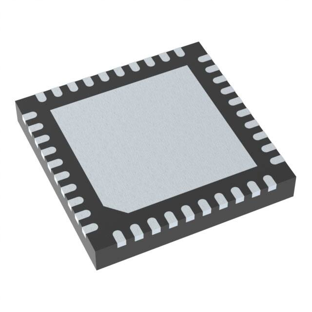


 工商网监
湘ICP备2023018690号
工商网监
湘ICP备2023018690号
