LT8610AX
42V, 3.5A Synchronous
Step-Down Regulator with
Operation to 175°C
DESCRIPTION
FEATURES
100% Tested at 175°C
nn ±2% Reference Accuracy Over –40°C to 175°C Range
nn Wide Input Voltage Range: 3.7V to 42V
nn Ultralow Quiescent Current Burst Mode® Operation
nn High Efficiency Synchronous Operation
nn 91% Eff. at 0.5A, at 175°C, 3.3V
OUT from 12VIN
nn 92% Eff. at 0.5A, at 175°C, 5V
OUT from 12VIN
nn Adjustable and Synchronizable Frequency: 200kHz
to 2.2MHz
nn No Thermal Shutdown
nn Internal Compensation
nn Output Soft-Start and Tracking
nn Power Good Flag
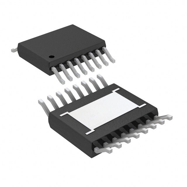
nn Small Thermally-Enhanced 16-Lead MSOP Package
nn
APPLICATIONS
nn
Oil and Gas Exploration
The LT®8610AX is a compact, high efficiency, high speed
synchronous monolithic step-down switching regulator
rated to 175°C junction temperature. The LT8610AX is
100% tested a 175°C. Top and bottom power switches
are included with all necessary circuitry to minimize the
need for external components. Low ripple Burst Mode
operation enables high efficiency across a wide range of
output currents while keeping the output ripple low. A SYNC
pin allows synchronization to an external clock. Internal
compensation with peak current mode topology allows
the use of small inductors and results in fast transient
response and good loop stability. The EN/UV pin has an
accurate 1V threshold and can be used to program VIN
undervoltage lockout or to shut down the LT8610AX. A
capacitor on the TR/SS pin programs the output voltage
ramp rate during startup while the PG flag signals when
VOUT is within ±9% of the programmed output voltage
as well as fault conditions. The LT8610AX is available in
small 16-lead MSOP package with exposed pad for low
thermal resistance.
L, LT, LTC, LTM, Linear Technology, the Linear logo and Burst Mode are registered trademarks
of Linear Technology Corporation. All other trademarks are the property of their respective
owners.
TYPICAL APPLICATION
3.3V Step-Down Converter
Efficiency
at 175°C
Efficiency
at 175°C
100
VIN
4.7µF
0.1µF 4.7µH
EN/UV
LT8610AX
100nF
SW
BIAS
TR/SS
49.9k
PG
1µF
100k
FB
INTVCC
RT
90
BST
GND
10pF
SYNC
80
70
60
50
40
30
20
41.2k
60.4k
fSW = 700kHz
47µF
×2
1210
X7R
VOUT
3.3V
3.5A
EFFICIENCY (%)
VIN
3.7V TO 42V
8610AX TA01a
TA = 175°C
12VIN
10
0
1
10
100
1k
LOAD CURRENT (mA)
10k
8610AX TA01b
8610axf
For more information www.linear.com/LT8610AX
1
�LT8610AX
ABSOLUTE MAXIMUM RATINGS
PIN CONFIGURATION
(Note 1)
VIN, EN/UV, PG...........................................................42V
BIAS...........................................................................30V
FB, TR/SS Voltage ......................................................4V
SYNC Voltage ..............................................................6V
Operating Junction Temperature Range (Note 2)
LT8610AX............................................... –40 to 175°C
Storage Temperature Range.......................–65 to 150°C
TOP VIEW
SYNC
TR/SS
RT
EN/UV
VIN
VIN
NC
GND
1
2
3
4
5
6
7
8
16
15
14
13
12
11
10
9
17
GND
FB
PG
BIAS
INTVCC
BST
SW
SW
SW
MSE PACKAGE
16-LEAD PLASTIC MSOP
θJA = 40°C/W, θJC(PAD) = 10°C/W
EXPOSED PAD (PIN 17) IS GND, MUST BE SOLDERED TO PCB
ORDER INFORMATION
(http://www.linear.com/product/LT8610AX#orderinfo)
LEAD FREE FINISH
TAPE AND REEL
PART MARKING
PACKAGE DESCRIPTION
TEMPERATURE RANGE
LT8610AXMSE#PBF
LT8610AXMSE#TRPBF
8610AX
16-Lead Plastic MSOP
–40°C to 175°C
Consult LTC Marketing for parts specified with wider operating temperature ranges.
For more information on lead free part marking, go to: http://www.linear.com/leadfree/
For more information on tape and reel specifications, go to: http://www.linear.com/tapeandreel/. Some packages are available in 500 unit reels through
designated sales channels with #TRMPBF suffix.
ELECTRICAL CHARACTERISTICS
The l denotes the specifications which apply over the full operating
temperature range, otherwise specifications are at TA = 25°C.
PARAMETER
CONDITIONS
MIN
Minimum Input Voltage
VIN Current in Regulation
VOUT = 0.97V, VIN = 6V, Output Load = 100μA
VOUT = 0.97V, VIN = 6V, Output Load = 1mA
Feedback Reference Voltage
VIN = 12V
TYP
MAX
l
3.2
3.7
V
l
l
26
230
100
400
μA
μA
V
V
l
0.966
0.950
0.972
0.970
0.978
0.990
UNITS
Oscillator Frequency
RT = 60.4k
l
665
700
735
kHz
PG Upper Threshold Offset from VFB
VFB Falling
l
6
9
12
%
PG Lower Threshold Offset from VFB
VFB Rising
l
–12
–9
–6
%
Note 1: Stresses beyond those listed under Absolute Maximum Ratings
may cause permanent damage to the device. Exposure to any Absolute
Maximum Rating condition for extended periods may affect device
reliability and lifetime.
Note 2: Devices are 100% tested at 175°C to the limits shown. For normal
operating temperature range specifications, please see the LT8610A/
LT8610AB data sheet. The LT8610AX performance is based on the
LT8610AB.
2
Note 3. The LT8610AX is guaranteed over the full –40°C to 175°C
operating junction temperature range. High junction temperatures degrade
operating lifetimes. Operating lifetime is derated at junction temperatures
greater than 125°C. The LT8610AX has no thermal shutdown.
8610axf
For more information www.linear.com/LT8610AX
�LT8610AX
TYPICAL PERFORMANCE CHARACTERISTICS
Reference
Reference Voltage
Voltage
Reference
Reference Voltage
Voltage at
at 175°C
175C
45
1000
LOAD = 0.5A
100
N = 347
µ = 968.5
σ = 3.33
90
960
950
30
EFFICIENCY (%)
970
15
940
25
50
75 100 125 150
TEMPERATURE (°C)
175
200
36VIN
50
40
30
12VIN
80
24VIN
70
EFFICIENCY (%)
85
90
36VIN
80
75
70
36VIN
40
30
160
120
100
80
60
40
0.1
1
10
100
LOAD CURRENT (mA)
15
20
25
30
INPUT VOLTAGE (V)
36VIN
75
1k
10k
60
100 200 300 400 500 600 700 800 900 1000
LOAD CURRENT (mA)
8610AX G06
Power Up at 175°C
EN
5V/DIV
VIN
10V/DIV
VOUT
2V/DIV
VOUT
2V/DIV
PG
2V/DIV
SS
2V/DIV
PG
2V/DIV
SS
2V/DIV
10ms/DIV
20
10
24VIN
TA = 175°C
140
5
80
EN Cycling at 175°C
TA = 175°C
FRONT PAGE APP
3.3VOUT IN REGULATION
180
85
8610AX G05
No Load Input Current at 175°C
200
TA = 175°C
fSW = 700kHz
65
0
0.01
8610AX G04
12VIN
70
10
60
100 200 300 400 500 600 700 800 900 1000
LOAD CURRENT (mA)
10k
90
24VIN
20
65
0
95
12VIN
50
1k
OUT
100
TA = 175°C
fSW = 700kHz
60
1
10
100
LOAD CURRENT (mA)
Efficiency at 175°C, VOUT = 5V
OUT
EFFICIENCY (%)
100
TA = 175°C
fSW = 700kHz
90
0.1
8610AX G03
Efficiency
Efficiency at
at 175°C,
175°C, VVOUT == 5V
5V
OUT
95
0
0.01
8610AX G02
Efficiency at 175°C, VOUT = 3.3V
100
EFFICIENCY (%)
24VIN
60
10
0
950 955 960 965 970 975 980 985 990
REFERENCE VOLTAGE (mV)
8610AX G01
INPUT CURRENT (uA)
12VIN
70
20
930
920
OUT
TA = 175°C
fSW = 700kHz
80
980
NUMBER OF PARTS
REFERENCE VOLTAGE (mV)
990
Efficiency
Efficiency at
at 175°C,
175°C, VVOUT ==3.3V
3.3V
35
8610AX G08
TA = 175°C
10ms/DIV
8610AX G09
40
8610AX G07
8610axf
For more information www.linear.com/LT8610AX
3
�LT8610AX
PIN FUNCTIONS
SYNC (Pin 1): External Clock Synchronization Input.
Ground this pin for low ripple Burst Mode operation at low
output loads. Tie to a clock source for synchronization to
an external frequency. Apply a DC voltage of 3V or higher
or tie to INTVCC for pulse-skipping mode. When in pulseskipping mode, the IQ will increase to several hundred µA.
Do not float this pin.
SW (Pins 9, 10, 11): The SW pins are the outputs of the
internal power switches. Tie these pins together and connect them to the inductor and boost capacitor. This node
should be kept small on the PCB for good performance.
TR/SS (Pin 2): Output Tracking and Soft-Start Pin. This
pin allows user control of output voltage ramp rate during
start-up. A TR/SS voltage below 0.97V forces the LT8610AX
to regulate the FB pin to equal the TR/SS pin voltage. When
TR/SS is above 0.97V, the tracking function is disabled
and the internal reference resumes control of the error
amplifier. An internal 2.2μA pull-up current from INTVCC on
this pin allows a capacitor to program output voltage slew
rate. This pin is pulled to ground with an internal 230Ω
MOSFET during shutdown and fault conditions; use a series
resistor if driving from a low impedance output. This pin
may be left floating if the tracking function is not needed.
INTVCC (Pin 13): Internal 3.4V Regulator Bypass Pin.
The internal power drivers and control circuits are powered from this voltage. INTVCC maximum output current is 20mA. Do not load the INTVCC pin with external
circuitry. INTVCC current will be supplied from BIAS if
VBIAS > 3.1V, otherwise current will be drawn from VIN.
Voltage on INTVCC will vary between 2.8V and 3.4V when
VBIAS is between 3.0V and 3.6V. Decouple this pin to power
ground with at least a 1μF low ESR ceramic capacitor
placed close to the IC.
RT (Pin 3): A resistor is tied between RT and ground to
set the switching frequency.
EN/UV (Pin 4): The LT8610AX is shut down when this
pin is low and active when this pin is high. The hysteretic
threshold voltage is 1.00V going up and 0.96V going
down. Tie to VIN if the shutdown feature is not used. An
external resistor divider from VIN can be used to program
a VIN threshold below which the LT8610AX will shut down.
VIN (Pins 5, 6): The VIN pins supply current to the LT8610AX
internal circuitry and to the internal topside power switch.
These pins must be tied together and be locally bypassed.
Be sure to place the positive terminal of the input capacitor as close as possible to the VIN pins, and the negative
capacitor terminal as close as possible to the GND pins.
NC (Pin 7): No Connect. This pin is not connected to
internal circuitry.
4
BST (Pin 12): This pin is used to provide a drive voltage,
higher than the input voltage, to the topside power switch.
Place a 0.1µF boost capacitor as close as possible to the IC.
BIAS (Pin 14): The internal regulator will draw current from
BIAS instead of VIN when BIAS is tied to a voltage higher
than 3.1V. For output voltages of 3.3V and above this pin
should be tied to VOUT. If this pin is tied to a supply other
than VOUT use a 1µF local bypass capacitor on this pin.
PG (Pin 15): The PG pin is the open-drain output of an
internal comparator. PG remains low until the FB pin is
within ±9% of the final regulation voltage, and there are
no fault conditions. PG is valid when VIN is above 3.4V,
regardless of EN/UV pin state.
FB (Pin 16): The LT8610AX regulates the FB pin to 0.970V.
Connect the feedback resistor divider tap to this pin. Also,
connect a phase lead capacitor between FB and VOUT.
Typically, this capacitor is 4.7pF to 10pF.
GND (Pin 8, Exposed Pad Pin 17): Ground. These pins
are the return path of the internal bottom-side switch and
must be tied together. Place the negative terminal of the
input capacitor as close to the GND pin and exposed pad
as possible. The exposed pad must be soldered to the PCB
in order to lower the thermal resistance.
8610axf
For more information www.linear.com/LT8610AX
�LT8610AX
APPLICATIONS INFORMATION
For Application Information, Block Diagram, and Typical Performance Curves from –40°C to 150°C range, please see
the LT8610A/LT8610AB Series data sheet. The LT8610AX will perform similarly to the LT8610AB. The LT8610AX
has no thermal shutdown.
PACKAGE DESCRIPTION
Please refer to http://www.linear.com/product/LT8610AX#packaging for the most recent package drawings.
MSE Package
16-Lead Plastic MSOP, Exposed Die Pad
(Reference LTC DWG # 05-08-1667 Rev F)
BOTTOM VIEW OF
EXPOSED PAD OPTION
2.845 ±0.102
(.112 ±.004)
5.10
(.201)
MIN
2.845 ±0.102
(.112 ±.004)
0.889 ±0.127
(.035 ±.005)
8
1
1.651 ±0.102
(.065 ±.004)
1.651 ±0.102 3.20 – 3.45
(.065 ±.004) (.126 – .136)
0.305 ±0.038
(.0120 ±.0015)
TYP
16
0.50
(.0197)
BSC
4.039 ±0.102
(.159 ±.004)
(NOTE 3)
RECOMMENDED SOLDER PAD LAYOUT
0.254
(.010)
0.35
REF
0.12 REF
DETAIL “B”
CORNER TAIL IS PART OF
DETAIL “B” THE LEADFRAME FEATURE.
FOR REFERENCE ONLY
9
NO MEASUREMENT PURPOSE
0.280 ±0.076
(.011 ±.003)
REF
16151413121110 9
DETAIL “A”
0° – 6° TYP
3.00 ±0.102
(.118 ±.004)
(NOTE 4)
4.90 ±0.152
(.193 ±.006)
GAUGE PLANE
0.53 ±0.152
(.021 ±.006)
DETAIL “A”
1.10
(.043)
MAX
0.18
(.007)
SEATING
PLANE
0.17 – 0.27
(.007 – .011)
TYP
1234567 8
0.50
(.0197)
BSC
NOTE:
1. DIMENSIONS IN MILLIMETER/(INCH)
2. DRAWING NOT TO SCALE
3. DIMENSION DOES NOT INCLUDE MOLD FLASH, PROTRUSIONS OR GATE BURRS.
MOLD FLASH, PROTRUSIONS OR GATE BURRS SHALL NOT EXCEED 0.152mm (.006") PER SIDE
4. DIMENSION DOES NOT INCLUDE INTERLEAD FLASH OR PROTRUSIONS.
INTERLEAD FLASH OR PROTRUSIONS SHALL NOT EXCEED 0.152mm (.006") PER SIDE
5. LEAD COPLANARITY (BOTTOM OF LEADS AFTER FORMING) SHALL BE 0.102mm (.004") MAX
6. EXPOSED PAD DIMENSION DOES INCLUDE MOLD FLASH. MOLD FLASH ON E-PAD SHALL
NOT EXCEED 0.254mm (.010") PER SIDE.
0.86
(.034)
REF
0.1016 ±0.0508
(.004 ±.002)
MSOP (MSE16) 0213 REV F
8610axf
Information furnished by Linear Technology Corporation is believed to be accurate and reliable.
However, no responsibility is assumed for its use. Linear Technology Corporation makes no representation that the interconnection
of itsinformation
circuits as described
herein will not infringe on existing patent rights.
For more
www.linear.com/LT8610AX
5
�LT8610AX
RELATED PARTS
PART NUMBER
DESCRIPTION
COMMENTS
PACKAGE
LT1007X
Low Noise 200°C Op Amp
Low Noise, High Speed Precision Operational Amplifier
8-Lead TO-5 Metal Can
LT580X
200°C, 2.5V Voltage Reference
Ultra Low Drift, Curvature Corrected Reference
3-Lead TO-52 Metal Can
LT581X
200°C, 10V Voltage Reference
Ultra Low Drift, Curvature Corrected Reference
3-Lead TO-39 Metal Can
LT582X
200°C, 5V Voltage Reference
Ultra Low Drift, Curvature Corrected Reference
3-Lead TO-39 Metal Can
6
8610axf
Linear Technology Corporation
1630 McCarthy Blvd., Milpitas, CA 95035-7417
For more information www.linear.com/LT8610AX
(408) 432-1900 ● FAX: (408) 434-0507
●
www.linear.com/LT8610AX
LT 0416 • PRINTED IN USA
LINEAR TECHNOLOGY CORPORATION 2016
�


 工商网监
湘ICP备2023018690号
工商网监
湘ICP备2023018690号
