LT8645S/LT8646S
65V, 8A Synchronous
Step-Down Silent Switcher 2
with 2.5µA Quiescent Current
DESCRIPTION
FEATURES
Silent Switcher®2 Architecture
n Ultralow EMI Emissions on Any PCB
n Eliminates PCB Layout Sensitivity
n Internal Bypass Capacitors Reduce Radiated EMI
n Optional Spread Spectrum Modulation
n High Efficiency at High Frequency
n Up to 95% Efficiency at 1MHz, 12V to 5V
IN
OUT
n Up to 94% Efficiency at 2MHz, 12V to 5V
IN
OUT
n Wide Input Voltage Range: 3.4V to 65V
n Ultralow Quiescent Current Burst Mode Operation
n 2.5μA I Regulating 12V to 3.3V
Q
IN
OUT (LT8645S)
n Output Ripple < 10mV
P-P
n External Compensation: Fast Transient Response
and Current Sharing (LT8646S)
n Fast Minimum Switch On-Time: 40ns
n Low Dropout Under All Conditions: 60mV at 1A
n Adjustable and Synchronizable: 200kHz to 2.2MHz
n Peak Current Mode Operation
n Output Soft-Start and Tracking
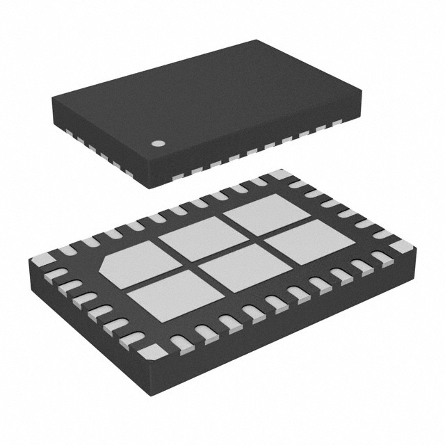
n Small 32-Lead 6mm × 4mm LQFN Package
n AEC-Q100 Qualified for Automotive Applications
n
APPLICATIONS
The LT®8645S/LT8646S synchronous step-down regulator
features second generation Silent Switcher architecture
designed to minimize EMI emissions while delivering high
efficiency at high switching frequencies. This includes the
integration of bypass capacitors to optimize all the fast
current loops inside and make it easy to achieve advertised
EMI performance by eliminating layout sensitivity.
The fast, clean, low-overshoot switching edges enable
high efficiency operation even at high switching frequencies, leading to a small overall solution size. Peak current
mode control with a 40ns minimum on-time allows high
step-down ratios even at high switching frequencies. The
LT8646S has external compensation to enable current
sharing and fast transient response at high switching
frequencies.
Burst Mode® operation enables ultralow standby current
consumption, pulse-skipping mode allows full switching
frequency at lower output loads, or spread spectrum
operation can further reduce EMI emissions.
INTERNAL CAPS
VC COMP
150°C GRADE
LT8645S
Yes
Internal
No
LT8646S
Yes
External
No
n
LT8645S-2*
No
Internal
Yes
n
*See LT8645S-2 Data Sheet
Automotive and Industrial Supplies
General Purpose Step-Down
n GSM Power Supplies
All registered trademarks and trademarks are the property of their respective owners. Protected
by U.S. patents, including 8823345.
TYPICAL APPLICATION
12VIN to 5VOUT Efficiency
5V 8A Step-Down Converter
2.2µH
VIN
EN/UV
BIAS
LT8645S
RT
2.2pF
1M
100µF
FB
4.0
95
3.5
90
85
2.5
80
2.0
GND
243k
8645S TA01a
fSW = 1MHz
1.5
75
70
41.2k
3.0
EFFICIENCY
POWER LOSS
65
60
1
2
POWER LOSS (W)
4.7µF
VOUT
5V
8A
SW
EFFICIENCY (%)
VIN
5.5V TO 65V
100
1.0
1MHz, L = 2.2µH 0.5
2MHz, L = 1µH
0
3
4
5
6
7
8
LOAD CURRENT (A)
8645S TA01b
Rev. B
Document Feedback
For more information www.analog.com
1
�LT8645S/LT8646S
ABSOLUTE MAXIMUM RATINGS
(Note 1)
VIN, EN/UV.................................................................65V
PG..............................................................................42V
BIAS...........................................................................25V
FB, TR/SS ...................................................................4V
SYNC/MODE Voltage ..................................................6V
Operating Junction Temperature Range (Note 2)
LT8645SE/LT8646SE.......................... –40°C to 125°C
LT8645SI/LT8646SI........................... –40°C to 125°C
Storage Temperature Range................... –65°C to 150°C
Maximum Reflow (Package Body) Temperature.... 260°C
PIN CONFIGURATION
LT8645S
LT8646S
PG
GND
TR/SS
SYNC/MODE
CLKOUT
FB
PG
VC
TR/SS
SYNC/MODE
CLKOUT
32
31
30
29
28
27
32
31
30
29
28
27
23 VIN
VIN
4
22 VIN
VIN
5
21 VIN
VIN
6
20 NC
NC
7
19 GND
GND
8
18 GND
GND
9
17 GND
GND
10
VIN
4
VIN
5
VIN
6
NC
7
GND
8
GND
9
GND
10
35
GND
36
GND
11
12
13
14
15
16
SW
SW
SW
SW
SW
38
GND
BST
37
GND
33
GND
25 EN/UV
34
GND
24 NC
23 VIN
35
GND
22 VIN
36
GND
21 VIN
20 NC
37
GND
19 GND
38
GND
18 GND
17 GND
11
12
13
14
15
16
SW
3
3
34
GND
SW
NC
NC
33
GND
26 RT
SW
24 NC
25 EN/UV
SW
2
26 RT
2
SW
1
1
BST
BIAS
INTVCC
BIAS
INTVCC
LQFN PACKAGE
32-LEAD (6mm × 4mm × 0.94mm)
JEDEC BOARD: θJA = 30°C/W, ΨJT = 0.6°C/W,
θJCTOP = 28.5°C/W, θJC(PAD) = 4.4°C/W (NOTE 3)
DEMO BOARD: θJA = 17°C/W
EXPOSED PADS (PINS 33-38) ARE GND, SHOULD BE SOLDERED TO PCB
2
TOP VIEW
FB
TOP VIEW
LQFN PACKAGE
32-LEAD (6mm × 4mm × 0.94mm)
JEDEC BOARD: θJA = 30°C/W, ΨJT = 0.6°C/W,
θJCTOP = 28.5°C/W, θJC(PAD) = 4.4°C/W (NOTE 3)
DEMO BOARD: θJA = 17°C/W
EXPOSED PADS (PINS 33-38) ARE GND, SHOULD BE SOLDERED TO PCB
Rev. B
For more information www.analog.com
�LT8645S/LT8646S
ORDER INFORMATION
PART NUMBER
PART MARKING*
LT8645SEV#PBF
LT8645SIV#PBF
LT8646SEV#PBF
LT8646SIV#PBF
MSL
RATING
FINISH CODE
PAD FINISH
PACKAGE TYPE***
e4
Au (RoHS)
LQFN (Laminate Package
with QFN Footprint)
3
–40°C to 125°C
e4
Au (RoHS)
LQFN (Laminate Package
with QFN Footprint)
3
–40°C to 125°C
8645SV
8646SV
TEMPERATURE RANGE
AUTOMOTIVE PRODUCTS**
LT8645SEV#WPBF
LT8645SIV#WPBF
LT8646SEV#WPBF
LT8646SIV#WPBF
8645SV
8646SV
• Contact the factory for parts specified with wider operating temperature
ranges. *Pad or ball finish code is per IPC/JEDEC J-STD-609.
• Recommended LGA and BGA PCB Assembly and Manufacturing
Procedures
• LGA and BGA Package and Tray Drawings
Parts ending with PBF are RoHS and WEEE compliant. ***The LT8645S/LT8646S package has the same footprint as a standard 6mm × 4mm QFN Package.
**Versions of this part are available with controlled manufacturing to support the quality and reliability requirements of automotive applications. These
models are designated with a #W suffix. Only the automotive grade products shown are available for use in automotive applications. Contact your
local Analog Devices account representative for specific product ordering information and to obtain the specific Automotive Reliability reports for
these models.
ELECTRICAL
CHARACTERISTICS
The
l denotes the specifications which apply over the full operating
temperature range, otherwise specifications are at TA = 25°C.
PARAMETER
CONDITIONS
TYP
MAX
l
3.0
3.4
V
l
0.9
0.9
3
10
µA
µA
l
1.7
1.7
4
10
µA
µA
l
230
230
290
340
µA
µA
VEN/UV = 2V, VFB > 0.97V, VSYNC = 0V, VBIAS = 5V
16
25
µA
LT8646S BIAS Quiescent Current in Sleep
VEN/UV = 2V, VFB > 0.97V, VSYNC = 0V, VBIAS = 5V
200
260
µA
LT8645S VIN Quiescent Current when Active
VEN/UV = 2V, VFB > 0.97V, VSYNC = 2V, RT = 60.4k, VBIAS = 0V
0.4
0.6
mA
0.6
0.8
mA
17
200
60
400
µA
µA
0.970
0.970
0.976
0.982
V
V
0.004
0.025
%/V
20
nA
Minimum Input Voltage
VIN Quiescent Current in Shutdown
MIN
VEN/UV = 0V
LT8645S VIN Quiescent Current in Sleep
(Internal Compensation)
VEN/UV = 2V, VFB > 0.97V, VSYNC = 0V
LT8646S VIN Quiescent Current in Sleep
(External Compensation)
VEN/UV = 2V, VFB > 0.97V, VSYNC = 0V, VBIAS = 0V
UNITS
LT8646S VIN Quiescent Current when Active
VEN/UV = 2V, VFB > 0.97V, VSYNC = 2V, RT = 60.4k, VBIAS = 0V
LT8645S VIN Current in Regulation
VOUT = 0.97V, VIN = 6V, ILOAD = 100µA, VSYNC = 0V
VOUT = 0.97V, VIN = 6V, ILOAD = 1mA, VSYNC = 0V
l
l
Feedback Reference Voltage
VIN = 6V
VIN = 6V
l
Feedback Voltage Line Regulation
VIN = 4.0V to 42V
l
Feedback Pin Input Current
VFB = 1V
LT8646S Error Amp Transconductance
VC = 1.25V
1.7
mS
350
V/V
LT8646S VC Source Current
VFB = 0.77V, VC = 1.25V
350
µA
LT8646S VC Sink Current
VFB = 1.17V, VC = 1.25V
350
µA
0.964
0.958
–20
LT8646S Error Amp Gain
Rev. B
For more information www.analog.com
3
�LT8645S/LT8646S
ELECTRICAL
CHARACTERISTICS
The
l denotes the specifications which apply over the full operating
temperature range, otherwise specifications are at TA = 25°C.
PARAMETER
CONDITIONS
MIN
LT8646S VC Pin to Switch Current Gain
BIAS Pin Current Consumption
VBIAS = 3.3V, fSW = 2MHz
Minimum On-Time
ILOAD = 2A, SYNC = 0V
ILOAD = 2A, SYNC = 2V
l
l
Minimum Off-Time
Oscillator Frequency
RT = 221k
RT = 60.4k
RT = 18.2k
Top Power NMOS On-Resistance
ISW = 1A
l
l
l
180
665
1.8
l
Bottom Power NMOS On-Resistance
VINTVCC = 3.4V, ISW = 1A
Bottom Power NMOS Current Limit
VINTVCC = 3.4V
SW Leakage Current
VIN = 42V, VSW = 0V, 42V
EN/UV Pin Threshold
EN/UV Rising
10.5
V
22
mA
40
35
65
60
ns
ns
80
110
ns
210
700
1.95
240
735
2.1
kHz
kHz
MHz
14
mΩ
17.5
0.95
13.5
A
1.5
µA
1.01
1.07
V
45
EN/UV Pin Current
VEN/UV = 2V
PG Upper Threshold Offset from VFB
VFB Falling
l
5
PG Lower Threshold Offset from VFB
–20
VFB Rising
l
–10.5
PG Hysteresis
A
mΩ
11
–1.5
l
EN/UV Pin Hysteresis
mV
20
nA
7.5
10
%
–8
–5.5
%
0.4
VPG = 3.3V
–40
PG Pull-Down Resistance
VPG = 0.1V
l
SYNC/MODE Threshold
SYNC/MODE DC and Clock Low Level Voltage
SYNC/MODE Clock High Level Voltage
SYNC/MODE DC High Level Voltage
l
l
l
Spread Spectrum Modulation
Frequency Range
RT = 60.4k, VSYNC = 3.3V
Spread Spectrum Modulation Frequency
VSYNC = 3.3V
TR/SS Source Current
l
Fault Condition, TR/SS = 0.1V
Note 1: Stresses beyond those listed under Absolute Maximum Ratings
may cause permanent damage to the device. Exposure to any Absolute
Maximum Rating condition for extended periods may affect device
reliability and lifetime.
Note 2: The LT8645SE/LT8646SE is guaranteed to meet performance
specifications from 0°C to 125°C junction temperature. Specifications over
the –40°C to 125°C operating junction temperature range are assured by
design, characterization, and correlation with statistical process controls.
The LT8645SI/LT8646SI is guaranteed over the full –40°C to 125°C
operating junction temperature range.
The junction temperature (TJ, in °C) is calculated from the ambient
temperature (TA in °C) and power dissipation (PD, in Watts) according to
the formula:
TJ = TA + (PD • θJA)
where θJA (in °C/W) is the package thermal impedance.
4
2.6
25
8.5
UNITS
A/V
36
Top Power NMOS Current Limit
TR/SS Pull-Down Resistance
MAX
8
LT8646S VC Clamp Voltage
PG Leakage
TYP
0.7
2.2
1.2
%
40
nA
750
2000
Ω
0.9
1.2
2.55
1.4
2.9
V
V
V
24
%
2.5
kHz
1.9
2.6
µA
220
Ω
Note 3: θ values determined per JEDEC 51-7, 51-12. See Applications
Information Section for information on improving the thermal resistance
and for actual temperature measurements of a demo board in typical
operating conditions.
Note 4: This IC includes overtemperature protection that is intended to
protect the device during overload conditions. Junction temperature will
exceed 150°C when overtemperature protection is active. Continuous
operation above the specified maximum operating junction temperature
will reduce lifetime.
Rev. B
For more information www.analog.com
�LT8645S/LT8646S
TYPICAL PERFORMANCE CHARACTERISTICS
12VIN to 3.3VOUT Efficiency
vs Frequency
4.0
100
3.5
95
EFFICIENCY
3.0
2.0
1.5
75
L = XEL6060 1.0
500kHz, L = 2.7µH
1MHz, L = 2.2µH
2MHz, L = 1µH
60
1
2
3
4
5
6
LOAD CURRENT (A)
7
8
2.0
80
75
70
0.5
65
0
60
1.5
POWER LOSS
1
2
L = XEL6060 1.0
500kHz, L = 2.7µH
1MHz, L = 1.5µH 0.5
2MHz, L = 0.82µH
0
3
4
5
6
7
8
LOAD CURRENT (A)
8645S G01
65
1.2
2
3
4
5
LOAD CURRENT (A)
EFFICIENCY (%)
EFFICIENCY (%)
1.6
1
60
50
VIN = 12V
VIN = 24V
VIN = 36V
VIN = 48V
40
VIN = 12V
0.8
VIN = 24V
VIN = 36V 0.4
VIN = 48V
0
6
7
8
30
20
0.01
90
80
80
60
VIN = 12V
VIN = 24V
VIN = 36V
VIN = 48V
fSW = 500kHz
L = WE–LHMI7050, 4.7µH
30
20
0.01
0.1
1
10
100
LOAD CURRENT (mA)
1000
8645S G07
EFFICIENCY (%)
EFFICIENCY (%)
90
70
7
8
0
OUT
1
10
100
LOAD CURRENT (mA)
60
50
VIN = 12V
VIN = 24V
VIN = 36V
VIN = 48V
fSW = 500kHz
L = WE–LHMI7050, 4.7µH
40
30
20
fSW = 500kHz
L = WE–LHMI7050, 4.7µH
0.1
70
10
0.1
1000
1
10
100
1000
LOAD CURRENT (mA)
8645S G06
8645S G05
100
40
3
4
5
6
LOAD CURRENT (A)
LT8646S Low Load Efficiency
at 5VOUT
70
LT8645S Low Load Efficiency at
3.3VOUT
50
2
0.4
80
8645S G04
100
1
0.8
8645S G03
80
POWER LOSS (W)
2.0
70
0
0
90
2.4
fSW = 500kHz
L = XEL6060, 2.7µH
POWER LOSS
90
80
POWER LOSS
50
3.6
2.8
50
55
1.2
VIN = 12V
VIN = 24V
VIN = 36V
VIN = 48V
60
100
85
55
1.6
65
100
3.2
60
2.0
70
4.0
90
75
2.4
75
LT8645S Low Load Efficiency
at 5VOUT
EFFICIENCY
95
2.8
fSW = 500kHz
L = XEL6060, 2.7µH
80
8645S G02
Efficiency at 3.3VOUT
100
3.6
3.2
85
EFFICIENCY (%)
65
2.5
4.0
EFFICIENCY
90
LT8646S Low Load Efficiency at
3.3V
LT8646S
OUT Low Load Efficiency at 3.3V OUT
94
VIN = 12V
92
70
60
50
VIN = 12V
VIN = 24V
VIN = 36V
VIN = 48V
40
30
fSW = 500kHz
L = WE–LHMI7050, 4.7µH
20
10
0.1
Efficiency vs Frequency
96
1
10
100
1000
LOAD CURRENT (mA)
8645S G08
EFFICIENCY (%)
POWER LOSS
EFFICIENCY (%)
80
3.5
95
3.0
EFFICIENCY
85
100
POWER LOSS (W)
2.5
90
4.0
POWER LOSS (W)
85
70
95
POWER LOSS (W)
EFFICIENCY (%)
90
Efficiency at 5VOUT
100
EFFICIENCY (%)
12VIN to 5VOUT Efficiency
vs Frequency
90
88
VIN = 24V
86
84
82
80
0.4
VOUT = 3.3V
ILOAD = 2A
L = XEL6060, 4.7µH
0.7
1
1.3
1.6
1.9
SWITCHING FREQUENCY (MHz)
2.2
8645S G09
Rev. B
For more information www.analog.com
5
�LT8645S/LT8646S
TYPICAL PERFORMANCE CHARACTERISTICS
Burst Mode Operation Efficiency
vs Inductor Value (LT8645S)
VIN = 12V
85
VIN = 24V
80
75
VOUT = 5V
ILOAD = 10mA
L = WE–LHMI7050
70
65
1
2
3
4
5
6
7
8
INDUCTOR VALUE (µH)
9
1.03
977
1.02
975
REFERENCE VOLTAGE (mV)
EFFICIENCY (%)
90
979
973
971
969
967
961
–50
–25
0
25
50
75
TEMPERATURE (°C)
100
0.05
0
0.10
0.00
–0.10
–0.20
–0.30
VOUT = 5V
VIN = 12V
VSYNC = 0V
VOUT = 5V
VIN = 12V
VSYNC = 0V
–0.40
8
–0.50
0
1
8645S G13
0.25
4.0
0.15
0.10
0.05
0
15
25
35
45
INPUT VOLTAGE (V)
55
65
8645S G16
6
–0.05
3
4
5
6
LOAD CURRENT (A)
7
8
–0.10
VOUT = 5V
ILOAD = 2A
5
15
25
35
45
INPUT VOLTAGE (V)
3.5
3.0
2.5
2.0
1.0
55
65
8645S G15
LT8646S No-Load Supply Current
225
VOUT = 3.3V
L = 4.7µH
IN-REGULATION
1.5
VOUT = 5V
ILOAD = 2A
5
0.00
VOUT = 5V
L = 4.7µH
IN REGULATION
200
INPUT CURRENT (µA)
0.20
–0.10
0.05
LT8645S No-Load Supply Current
4.5
INPUT CURRENT (µA)
CHANGE IN VOUT (%)
LT8646S
Line Regulation
Regulation
LT8646S Line
–0.05
2
0.10
8645S G14
0.30
125
0.15
CHANGE IN VOUT (%)
CHANGE IN VOUT (%)
CHANGE IN VOUT (%)
0.10
7
100
LT8645S Line Regulation
0.20
3
4
5
6
LOAD CURRENT (A)
0
25
50
75
TEMPERATURE (°C)
0.20
0.30
0.15
2
–25
8645S G12
0.40
1
EN FALLING
0.95
–50
125
LT8646S Load Regulation
LT8645S Load Regulation
0
0.98
8645S G11
0.20
–0.10
0.99
0.96
963
8645S G10
–0.05
1.00
0.97
965
10
EN RISING
1.01
EN THRESHOLD (V)
95
EN Pin Thresholds
Reference Voltage
100
175
150
125
100
75
50
0
10
20
30
40
50
INPUT VOLTAGE (V)
60
8645S G17
25
0
10
20
30
40
50
INPUT VOLTAGE (V)
60
8645S G18
Rev. B
For more information www.analog.com
�LT8645S/LT8646S
TYPICAL PERFORMANCE CHARACTERISTICS
Top FET Current Limit
vs Duty Cycle
Switch Drop vs Temperature
Top FET Current Limit
15.0
100
16
SWITCH CURRENT = 1A
14.5
80
13.5
13.0
12.5
12.0
SWITCH DROP (mV)
15
CURRENT LIMIT (A)
CURRENT LIMIT (A)
14.0
5% DC
14
13
60
TOP SWITCH
40
BOTTOM SWITCH
20
11.5
11.0
0.1
0.3
0.5
DUTY CYCLE
0.7
12
–50
0.9
–25
8645S G19
300
350
TOP SWITCH
150
100
BOTTOM SWITCH
1
2
3
4
5
SWITCH CURRENT (A)
6
250
200
150
100
0
7
35
ILOAD = 3A
VOUT = 0.97V
fSW = 2.2MHz
1
2
3
4
5
LOAD CURRENT (A)
700
690
680
670
0
25
50
75
TEMPERATURE (°C)
100
125
8645S G25
100
125
400
1000
800
600
400
FRONT PAGE APPLICATION
VIN = 12V
VOUT = 5V
200
0
0
25
50
75
TEMPERATURE (°C)
Minimum Load to Full Frequency
(Pulse-Skipping Mode)
LOAD CURRENT (mA)
710
–25
8645S G24
1200
720
–25
25
–50
7
Burst Frequency
RT = 60.4k
660
–50
6
8645S G23
SWITCHING FREQUENCY (kHz)
SWITCHING FREQUENCY (kHz)
40
30
0
125
BURST MODE OPERATION
PULSE–SKIPPING MODE
50
0
100
45
300
Switching Frequency
730
0
25
50
75
TEMPERATURE (°C)
Minimum On-Time
50
VIN = 5V
VOUT SET TO REGULATE AT 5V
L = XEL6060, 1µH
8645S G22
740
–25
8645S G21
MINIMUM ON-TIME (ns)
250
0
0
–50
125
Dropout Voltage
400
DROPOUT VOLTAGE (mV)
SWITCH DROP (mV)
Switch Drop vs Switch Current
50
100
8645S G20
350
200
0
25
50
75
TEMPERATURE (°C)
0
100
200
300
400
LOAD CURRENT (mA)
500
600
8645S G26
FRONT PAGE APPLICATION
350 VOUT = 5V
fSW = 1MHz
300 VSYNC = Float
250
200
150
100
50
0
5
15
25
35
45
INPUT VOLTAGE (V)
55
65
8645S G27
Rev. B
For more information www.analog.com
7
�LT8645S/LT8646S
TYPICAL PERFORMANCE CHARACTERISTICS
LT8646S Soft-Start Tracking
1.2
1.0
1.0
0.8
0.8
0.6
0.4
0.2
2.2
0.6
0.4
0.2
0
0.2
1.0
0.4 0.6 0.8
TR/SS VOLTAGE (V)
1.2
0
1.4
VSS = 0.5V
2.1
TR/SS PIN CURRENT (µA)
1.2
0
Soft-Start Current
LT8646S Soft-Start Tracking
FB VOLTAGE (V)
FB VOLTAGE (V)
LT8645S Soft-Start Tracking
2.0
1.9
1.8
1.7
1.6
1.5
0
0.2
0.4
0.6 0.8 1 1.2
TR/SS VOLTAGE (V)
1.4
1.4
–50
1.6
–25
0
25
50
75
TEMPERATURE (°C)
100
125
8645S G30
8645S G29
8645S G28
LT8646S Error Amp
Output
Current
LT8646S
Error Amp Output Current
PG High Thresholds
125
0
–125
–250
–375
–500
–200
VC = 1.25V
–100
0
100
FB PIN ERROR VOLTAGE (mV)
–6.0
9.5
9.0
8.5
FB RISING
8.0
7.5
FB FALLING
7.0
6.5
6.0
–50
200
–25
0
25
50
75
TEMPERATURE (°C)
100
125
–6.5
–7.0
–7.5
RT Programmed Switching
Frequency
–9.0
–9.5
–10.0
–50
225
75
50
3.2
3.0
2.8
2.6
0.6
1.4
1.8
1
SWITCHING FREQUENCY (MHz)
2.2
2.4
–50
125
14
13
12
11
VBIAS = 5V
VOUT = 5V
fSW = 1MHz
25
0
0.2
100
Bias Pin Current
BIAS PIN CURRENT (mA)
INPUT VOLTAGE (V)
100
0
25
50
75
TEMPERATURE (°C)
15
3.4
200
125
–25
8645S G33
Minimum Input Voltage
150
FB FALLING
–8.5
3.6
250
175
FB RISING
–8.0
8645S G32
8645S G31
RT PIN RESISTOR (kΩ)
PG THRESHOLD OFFSET FROM VREF (%)
250
PG THRESHOLD OFFSET FROM VREF (%)
375
VCC PIN CURRENT (µA)
PG Low Thresholds
10.0
500
–25
0
25
50
75
TEMPERATURE (°C)
100
125
8645S G35
10
5
15
25
35
45
INPUT VOLTAGE (V)
55
65
8645S G36
8645S G34
8
Rev. B
For more information www.analog.com
�LT8645S/LT8646S
TYPICAL PERFORMANCE CHARACTERISTICS
Bias Pin Current
30
VBIAS = 5V
VOUT = 5V
VIN = 12V
ILOAD = 1A
DC2468A DEMO BOARD
VIN = 12V, fSW = 500kHz
VIN = 24V, fSW = 500kHz
VIN = 12V, fSW = 2MHz
VIN = 24V, fSW = 2MHz
70
CASE TEMPERATURE RISE (°C)
25
BIAS PIN CURRENT (mA)
Case Temperature Rise
80
20
15
10
5
60
50
40
30
20
10
0
0.2
0.6
1
1.4
1.8
SWITCHING FREQUENCY (MHz)
0
2.2
0
1
2
3
4
5
6
LOAD CURRENT (A)
8645S G37
7
8
8645S G38
Switching Waveforms, Full
Frequency Continuous Operation
Switch Rising Edge
IL
1A/DIV
VSW
2V/DIV
VSW
5V/DIV
VIN = 12V
ILOAD = 3A
2ns/DIV
8645S G39
500ns/DIV
FRONT PAGE APPLICATION
12VIN TO 5VOUT AT 2A
Switching Waveforms, Burst
Mode Operation
Switching Waveforms
IL
500mA/DIV
IL
1A/DIV
VSW
5V/DIV
VSW
20V/DIV
10µs/DIV
FRONT PAGE APPLICATION
12VIN TO 5VOUT AT 10mA
VSYNC = 0V
8645S G40
8645S G41
500ns/DIV
FRONT PAGE APPLICATION
48VIN TO 5VOUT AT 2A
8645S G42
Rev. B
For more information www.analog.com
9
�LT8645S/LT8646S
TYPICAL PERFORMANCE CHARACTERISTICS
LT8645S Transient Response;
Internal
Internal Compensation
Compensation
LT8646S Transient Response;
External Compensation
ILOAD
2A/DIV
ILOAD
2A/DIV
VOUT
100mV/DIV
VOUT
100mV/DIV
20µs/DIV
8645S G43
20µs/DIV
2A TO 4A TRANSIENT
12VIN, 5VOUT, fSW = 2MHz
CC = 330pF, RC = 7.5k
COUT = 100µF, CLEAD = 4.7pF
2A TO 4A TRANSIENT
12VIN, 5VOUT, fSW = 2MHz
COUT = 100µF, CLEAD = 4.7pF
LT8645S Transient Response;
300mA (Burst Mode Operation) to
1.3A
Transient
to 1.3A
Transient
ILOAD
1A/DIV
VOUT
100mV/DIV
VOUT
100mV/DIV
VIN
2V/DIV
VOUT
2V/DIV
8645S G45
50µs/DIV
8645S G46
300mA TO 1.3A TRANSIENT
12VIN, 5VOUT, fSW = 2MHz
COUT = 100µF, CLEAD = 4.7pF
300mA TO 1.3A TRANSIENT
12VIN, 5VOUT, fSW = 2MHz
CC = 330pF, RC = 7.5k
COUT = 100µF, CLEAD = 4.7pF
Start-Up Dropout Performance
Start-Up Dropout Performance
VIN
VIN
2V/DIV
VOUT
100ms/DIV
2.5Ω LOAD
(2A IN REGULATION)
10
LT8646S Transient Response;
300mA (Burst Mode Operation) to
1.3A Transient
ILOAD
1A/DIV
50µs/DIV
8645S G44
VOUT
2V/DIV
8645S G47
VIN
VOUT
100ms/DIV
20Ω LOAD
(250mA IN REGULATION)
8645S G48
Rev. B
For more information www.analog.com
�LT8645S/LT8646S
TYPICAL PERFORMANCE CHARACTERISTICS
Conducted EMI Performance
60
50
AMPLITUDE (dBµV)
40
30
20
10
0
–10
–20
FIXED FREQUENCY MODE
SPREAD SPECTRUM MODE
–30
–40
0
3
6
9
12
15
18
FREQUENCY (MHz)
21
24
27
DC2468A DEMO BOARD
(WITH EMI FILTER INSTALLED)
14V INPUT TO 5V OUTPUT AT 4A, fSW = 2MHz
30
8645S G49
Radiated EMI Performance
(CISPR25 Radiated Emission Test with Class 5 Peak Limits)
50
VERTICAL POLARIZATION
PEAK DETECTOR
45
AMPLITUDE (dBµV/m)
40
35
30
25
20
15
10
5
CLASS 5 PEAK LIMIT
SPREAD SPECTRUM MODE
FIXED FREQUENCY MODE
0
–5
0
100
200
300
400
500
600
FREQUENCY (MHz)
700
800
900
1000
8645S G50
50
HORIZONTAL POLARIZATION
PEAK DETECTOR
45
AMPLITUDE (dBµV/m)
40
35
30
25
20
15
10
5
CLASS 5 PEAK LIMIT
SPREAD SPECTRUM MODE
FIXED FREQUENCY MODE
0
–5
0
100
200
300
400
500
600
FREQUENCY (MHz)
700
DC2468A DEMO BOARD
(WITH EMI FILTER INSTALLED)
14V INPUT TO 5V OUTPUT AT 4A, fSW = 2MHz
800
900
1000
8645S G51
Rev. B
For more information www.analog.com
11
�LT8645S/LT8646S
PIN FUNCTIONS
BIAS (Pin 1): The internal regulator will draw current from
BIAS instead of VIN when BIAS is tied to a voltage higher
than 3.1V. For output voltages of 3.3V to 25V this pin
should be tied to VOUT. If this pin is tied to a supply other
than VOUT use a 1µF local bypass capacitor on this pin.
If no supply is available, tie to GND. However, especially
for high input or high frequency applications, BIAS should
be tied to output or an external supply of 3.3V or above.
INTVCC (Pin 2): Internal 3.4V Regulator Bypass Pin. The
internal power drivers and control circuits are powered
from this voltage. INTVCC maximum output current is
25mA. Do not load the INTVCC pin with external circuitry.
INTVCC current will be supplied from BIAS if BIAS > 3.1V,
otherwise current will be drawn from VIN. Voltage on INTVCC
will vary between 2.8V and 3.4V when BIAS is between
3.0V and 3.6V. This pin should be floated.
NC (Pins 3, 7, 20, 24): No Connect. This pin is not connected to internal circuitry and can be tied anywhere on
the PCB, typically ground.
VIN (Pins 4, 5, 6, 21, 22, 23): The VIN pins supply current to the LT8645S/LT8646S internal circuitry and to
the internal topside power switch. These pins must be
tied together and be locally bypassed with a capacitor of
4.7µF or more. Be sure to place the positive terminal of
the input capacitor as close as possible to the VIN pins,
and the negative capacitor terminal as close as possible
to the GND pins. See the Applications Information section
for a sample layout.
GND (Pins 8, 9, 10, 17, 18, 19, Exposed Pad Pins
33–38): Ground. Place the negative terminal of the input
capacitor as close to the GND pins as possible. See the
Applications Information section for a sample layout. The
exposed pads should be soldered to the PCB for good
thermal performance. If necessary due to manufacturing
limitations Pins 33 to 38 may be left disconnected, however
thermal performance will be degraded.
SW (Pins 12, 13, 14, 15, 16): The SW pins are the outputs
of the internal power switches. Tie these pins together and
connect them to the inductor and boost capacitor. This node
should be kept small on the PCB for good performance
and low EMI.
EN/UV (Pin 25): The LT8645S/LT8646S is shut down
when this pin is low and active when this pin is high.
The hysteretic threshold voltage is 1.01V going up and
0.965V going down. Tie to VIN if the shutdown feature is
not used. An external resistor divider from VIN can be used
to program a VIN threshold below which the LT8645S/
LT8646S will shut down.
RT (Pin 26): A resistor is tied between RT and ground to
set the switching frequency.
CLKOUT (Pin 27): In pulse-skipping mode, spread spectrum, and synchronization modes, the CLKOUT pin will
provide a ~200ns wide pulse at the switch frequency. The
low and high levels of the CLKOUT pin are ground and
INTVCC respectively, and the drive strength of the CLKOUT
pin is several hundred ohms. In Burst Mode operation,
the CLKOUT pin will be low. Float this pin if the CLKOUT
function is not used.
SYNC/MODE (Pin 28): This pin programs four different
operating modes: 1) Burst Mode. Tie this pin to ground
for Burst Mode operation at low output loads—this will
result in ultralow quiescent current. 2) Pulse-skipping
mode. This mode offers full frequency operation down to
low output loads before pulse skipping occurs. Float this
pin for pulse-skipping mode. When floating, pin leakage
currents should be 3.1V
1µF OR GND
4.7pF
PINS NOT USED
IN THIS CIRCUIT:
BST, CLKOUT,
INTVCC, PG,
SYNC/MODE, TR/SS
RT
41.2k
866k
FB
47µF
×2
1210
X5R/X7R
1M
GND
8645S TA02
fSW = 1MHz
L: XEL6030
RELATED PARTS
PART NUMBER DESCRIPTION
COMMENTS
LT8640S
42V, 6A Synchronous Step-Down Silent Switcher 2 with 2.5µA Quiescent
Current
VIN(MIN) = 3.4V, VOUT(MAX) = 42V, VOUT(MIN) = 0.97V,
IQ = 2.5μA, ISD < 1μA, 4mm × 4mm LQFN-24
LT8640/
LT8640-1
42V, 5A, 96% Efficiency, 3MHz Synchronous MicroPower Step-Down
DC/DC Converter with IQ = 2.5µA
VIN(MIN) = 3.4V, VIN(MAX) = 42V, VOUT(MIN) = 0.97V,
IQ = 2.5μA, ISD < 1μA, 3mm × 4mm QFN-18
LT8641
65V, 3.5A, 95% Efficiency, 3MHz Synchronous MicroPower Step-Down
DC/DC Converter with IQ = 2.5µA
VIN(MIN) = 3V, VIN(MAX) = 65V, VOUT(MIN) = 0.81V,
IQ = 2.5μA, ISD < 1μA, 3mm × 4mm QFN-18
LT8609/
LT8609A
42V, 2A, 94% Efficiency, 2.2MHz Synchronous MicroPower Step-Down
DC/DC Converter with IQ = 2.5µA
VIN(MIN) = 3V, VIN(MAX) = 42V, VOUT(MIN) = 0.8V,
IQ = 2.5μA, ISD < 1μA, MSOP-10E
LT8610A/
LT8610AB
42V, 3.5A, 96% Efficiency, 2.2MHz Synchronous MicroPower Step-Down
DC/DC Converter with IQ = 2.5µA
VIN(MIN) = 3.4V, VIN(MAX) = 42V, VOUT(MIN) = 0.97V,
IQ = 2.5μA, ISD < 1μA, MSOP-16E
LT8610AC
42V, 3.5A, 96% Efficiency, 2.2MHz Synchronous MicroPower Step-Down
DC/DC Converter with IQ = 2.5µA
VIN(MIN) = 3V, VIN(MAX) = 42V, VOUT(MIN) = 0.8V,
IQ = 2.5μA, ISD < 1μA, MSOP-16E
LT8610
42V, 2.5A, 96% Efficiency, 2.2MHz Synchronous MicroPower Step-Down
DC/DC Converter with IQ = 2.5µA
VIN(MIN) = 3.4V, VIN(MAX) = 42V, VOUT(MIN) = 0.97V,
IQ = 2.5μA, ISD < 1μA, MSOP-16E
LT8611
42V, 2.5A, 96% Efficiency, 2.2MHz Synchronous MicroPower Step-Down
DC/DC Converter with IQ = 2.5µA and Input/Output Current Limit/Monitor
VIN(MIN) = 3.4V, VIN(MAX) = 42V, VOUT(MIN) = 0.97V,
IQ = 2.5μA, ISD < 1μA, 3mm × 5mm QFN-24
LT8616
42V, Dual 2.5A + 1.5A, 95% Efficiency, 2.2MHz Synchronous MicroPower
Step-Down DC/DC Converter with IQ = 5µA
VIN(MIN) = 3.4V, VIN(MAX) = 42V, VOUT(MIN) = 0.8V,
IQ = 5μA, ISD < 1μA, TSSOP-28E, 3mm × 6mm QFN-28
LT8620
65V, 2.5A, 94% Efficiency, 2.2MHz Synchronous MicroPower Step-Down
DC/DC Converter with IQ = 2.5µA
VIN(MIN) = 3.4V, VIN(MAX) = 65V, VOUT(MIN) = 0.97V,
IQ = 2.5μA, ISD < 1μA, MSOP-16E, 3mm × 5mm QFN-24
LT8614
42V, 4A, 96% Efficiency, 2.2MHz Synchronous Silent Switcher Step-Down VIN(MIN) = 3.4V, VIN(MAX) = 42V, VOUT(MIN) = 0.97V,
IQ = 2.5μA, ISD < 1μA, 3mm × 4mm QFN18
DC/DC Converter with IQ = 2.5µA
LT8612
42V, 6A, 96% Efficiency, 2.2MHz Synchronous MicroPower Step-Down
DC/DC Converter with IQ = 2.5µA
VIN(MIN) = 3.4V, VIN(MAX) = 42V, VOUT(MIN) = 0.97V,
IQ = 3.0μA, ISD < 1μA, 3mm × 6mm QFN-28
LT8613
42V, 6A, 96% Efficiency, 2.2MHz Synchronous MicroPower Step-Down
DC/DC Converter with Current Limiting
VIN(MIN) = 3.4V, VIN(MAX) = 42V, VOUT(MIN) = 0.97V,
IQ = 3.0μA, ISD < 1μA, 3mm × 6mm QFN-28
LT8602
42V, Quad Output (2.5A + 1.5A + 1.5A + 1.5A) 95% Efficiency, 2.2MHz
Synchronous MicroPower Step-Down DC/DC Converter with IQ = 25µA
VIN(MIN) = 3V, VIN(MAX) = 42V, VOUT(MIN) = 0.8V,
IQ = 2.5μA, ISD < 1μA, 6mm × 6mm QFN-40
30
Rev. B
04/20
www.analog.com
For more information www.analog.com
ANALOG DEVICES, INC. 2017-2020
�