LT8709
Negative Input
Synchronous Multi-Topology
DC/DC Controller
DESCRIPTION
FEATURES
Wide Negative Input Range: –4.5V to –80V
Rail-to-Rail Output Current Monitor and Control
Input Voltage Regulation for High Impedance Inputs
Power Good Indication Pin
MODE Pin for Forced CCM (Continuous Conduction
Mode) or Pulse-Skipping/DCM (Discontinuous
Conduction Mode) Operation
n Switching Frequency Up to 750kHz
n Easily Configurable as a Buck, Boost, Buck-Boost, or
Inverting Converter with a Single Feedback Pin
n Can be Synchronized to an External Clock
n High Gain EN/FBIN Pin Accepts Slowly Varying Input
Signals
n 20-Lead TSSOP Package
n
n
n
n
The LT®8709 is a synchronous PWM controller for negativeto-negative or negative-to-positive DC/DC conversion,
with rail-to-rail output current monitor and control. The
LT8709 is ideal for many local power supply designs. It
can be easily configured in buck, boost, buck-boost, and
inverting topologies with negative input voltages.
n
In addition, the LT8709’s rail-to-rail output current sense
allows the part to be configured in current limited applications such as battery or capacitor charging. The PG pin
is used for power good indication.
The LT8709’s switching frequency range can be set between
100kHz and 750kHz. The part may be clocked internally
at a frequency set by the resistor from the RT pin to the
–VIN pin, or it may be synchronized to an external clock.
APPLICATIONS
The LT8709 also features innovative EN/FBIN pin circuitry
that allows for slowly varying input signals and an adjustable undervoltage lockout function. The pin is also used for
input voltage regulation to avoid collapsing a high impedance input supply. Additional features such as frequency
foldback, thermal shutdown and soft-start are integrated.
The LT8709 is available in a 20-lead TSSOP package.
High Power Negative Input, Negative Output Power
Supplies
n High Power Negative Input, Positive Output Power
Supplies
n Telecom Equipment Power Supplies
n Cathodic Protection Power Supplies
n
L, LT, LTC, LTM, Linear Technology and the Linear logo are registered trademarks of Linear
Technology Corporation. All other trademarks are the property of their respective owners.
TYPICAL APPLICATION
250kHz, –16V to –30V Input to –12V/8.5A Output Buck
7.3µH
2mΩ
EN/FBIN
10k
BG
ISN
33k
ISP
LT8709
FBY
2.2µF
4.99k
INTVCC
100k
MODE
BIAS
PG
INTVEE
–VIN
–16V TO –30V
2.2µF
VC
SYNC
143k
–VIN
IMON
68nF
SS
3.5
70
3.0
60
2.5
50
2.0
40
1.5
30
1.0
20
0.5
0
1
2
5
7
3
4
6
LOAD CURRENT (A)
8
9
0
8709 TA01b
100pF
470nF
4.0
80
10
2.2µF
RT
4.5
90
EFFICIENCY (%)
62.5k
CSP CSN
100
POWER LOSS (W)
+
120µF
TG
GND
150µF
22µF
×3
–VIN
2.2µF
Efficiency and Power Loss
vs Load Current (–VIN = –24V)
VOUT
–12V
8.5A
+
10µF
×6
4mΩ
5.9k
2.2nF
8709 TA01a
8709fa
For more information www.linear.com/LT8709
1
�LT8709
ABSOLUTE MAXIMUM RATINGS
PIN CONFIGURATION
(Note 1)
GND Voltage with Reference to –VIN........... –0.3V to 80V
BIAS Voltage with Reference to –VIN.......... –0.3V to 80V
BG Voltage with Reference to –VIN..................... (Note 5)
TG Voltage with Reference to BIAS..................... (Note 5)
RT Voltage with Reference to –VIN................ –0.3V to 5V
SS Voltage with Reference to –VIN................ –0.3V to 3V
FBY Voltage with Reference to GND.............. –3V to 0.3V
VC Voltage with Reference to –VIN................ –0.3V to 2V
EN/FBIN Voltage with Reference to –VIN..... –0.3V to 80V
SYNC Voltage with Reference to –VIN........ –0.3V to 5.5V
PG Voltage with Reference to –VIN............... –0.3V to 7V
PG Current.............................................................. ±1mA
MODE Voltage with Reference to –VIN........ –0.3V to 40V
INTVCC Voltage with Reference to –VIN........ –0.3V to 7V
INTVEE Voltage with Reference to BIAS.............. (Note 5)
CSP Voltage with Reference to –VIN............. –0.3V to 2V
CSN Voltage with Reference to –VIN............. –0.3V to 2V
ISP Voltage.................................. ISN – 0.4V to ISN + 2V
ISN Voltage with Reference to –VIN............ –0.3V to 80V
IMON Voltage with Reference to –VIN........ –0.3V to 2.5V
Operating Junction Temperature Range
LT8709E............................................. –40°C to 125°C
LT8709I.............................................. –40°C to 125°C
Storage Temperature Range................... –65°C to 150°C
TOP VIEW
FBY
1
20 –VIN
VC
2
19 SYNC
SS
3
18 RT
PG
4
IMON
5
ISN
6
ISP
7
14 CSN
BIAS
8
13 GND
INTVEE
9
12 INTVCC
TG 10
17 MODE
21
–VIN
16 EN/FBIN
15 CSP
11 BG
FE PACKAGE
20-LEAD PLASTIC TSSOP
TJMAX = 125°C, θJA = 38°C/W, θJC = 10°C/W
EXPOSED PAD (PIN 21) IS –VIN, MUST BE SOLDERED TO PCB
ORDER INFORMATION
(http://www.linear.com/product/LT8709#orderinfo)
LEAD FREE FINISH
TAPE AND REEL
PART MARKING*
PACKAGE DESCRIPTION
TEMPERATURE RANGE
LT8709EFE#PBF
LT8709EFE#TRPBF
LT8709FE
20-Lead Plastic TSSOP
–40°C to 125°C
LT8709IFE#PBF
LT8709IFE#TRPBF
LT8709FE
20-Lead Plastic TSSOP
–40°C to 125°C
Consult LTC Marketing for parts specified with wider operating temperature ranges. *The temperature grade is identified by a label on the shipping container.
For more information on lead free part marking, go to: http://www.linear.com/leadfree/
For more information on tape and reel specifications, go to: http://www.linear.com/tapeandreel/. Some packages are available in 500 unit reels through
designated sales channels with #TRMPBF suffix.
2
8709fa
For more information www.linear.com/LT8709
�LT8709
ELECTRICAL CHARACTERISTICS
The l denotes the specifications which apply over the full operating
temperature range, otherwise specifications for each channel are at TA = 25°C. VGND – V–VIN = 12V, VEN/FBIN – V–VIN = 12V,
VBIAS – V–VIN = 12V, unless otherwise noted. Pin voltages have the following relations: FBY is relative to the GND pin, TG and INTVEE
to the BIAS pin, and all other pins to the –VIN pin, unless otherwise stated. Pin currents have the following relations: positive current is
denoted as current flowing into the pin; negative current is denoted as current flowing out of the pin, unless otherwise stated. (Note 2)
PARAMETER
CONDITIONS
MIN
Minimum Operating Input Voltage
VGND – V–VIN OR VBIAS – V–VIN
VGND – V–VIN, if VBIAS – V–VIN ≥ 4.5V
Quiescent Current, IGND,
Not Switching
VBIAS – V–VIN = 8V, VISN – V–VIN = 8V
VBIAS – V–VIN = 6.3V, VBIAS – VINTVEE = 6.3V
Quiescent Current in Shutdown, IGND
VEN/FBIN = 0V
EN/FBIN Minimum Input Voltage High,
Releases SS
EN/FBIN Minimum Input Voltage High,
Chip-On but SS Held Low
l
0
TYP
MAX
UNITS
4.25
4.5
V
V
4
5.5
5.5
7.5
mA
mA
0
1
µA
EN/FBIN Rising
l
1.64
1.7
1.76
V
EN/FBIN Rising
EN/FBIN Falling
l
l
1.22
1.18
1.3
1.26
1.38
1.34
V
V
EN/FBIN Minimum Input Voltage High
Hysteresis
44
EN/FBIN Input Voltage Low
Shutdown Mode
EN/FBIN Pin Bias Current
VEN/FBIN = 3V
VEN/FBIN = 1.7V
VEN/FBIN = 1.6V
VEN/FBIN = 0V
SS Charge Current
VSS = 50mV, Current Flowing Out of SS Pin
SS Low Detection Voltage
Part Exiting Undervoltage Lockout
SS Hi Detection Voltage
SS Rising
SS Falling
l
mV
0.3
V
µA
µA
µA
µA
14
13
44
19.5
17.5
0
60
25
22.5
0.1
l
7
10.1
13.8
µA
l
18
50
82
mV
1.5
1.3
1.8
1.7
2.1
2.05
SS Hi Detection Hysteresis
100
V
V
mV
Low Dropout Regulators, INTVCC and INTVEE
INTVCC Voltage
IINTVCC = 10mA
l
6.2
6.3
6.4
V
INTVCC Undervoltage Lockout
INTVCC Rising
INTVCC Falling
l
l
3.88
3.5
4
3.73
4.12
3.95
V
V
INTVCC Undervoltage Lockout Hysteresis
270
mV
255
280
mV
mV
INTVCC Dropout Voltage,
VGND – INTVCC
VGND – V–VIN = 6V, VBIAS – V–VIN = 0V, IINTVCC = 10mA
VGND – V–VIN = 0V, VBIAS – V–VIN = 6V, IINTVCC = 10mA
INTVCC Load Regulation
VGND – V–VIN = 0V, IINTVCC = 0mA to 80mA
VBIAS – V–VIN = 0V, IINTVCC = 0mA to 40mA
–0.44
–0.34
–2
–2
INTVCC Line Regulation
10V ≤ VGND – V–VIN ≤ 80V, VBIAS – V–VIN = 0V, IINTVCC = 10mA
10V ≤ VBIAS – V–VIN ≤ 80V, VGND – V–VIN = 0V, IINTVCC = 10mA
–0.003
–0.006
–0.03
–0.03
%/V
%/V
5
mA
INTVCC Maximum External Load Current
INTVEE Voltage, VBIAS – VINTVEE
IINTVEE = 10mA
l
INTVEE Undervoltage Lockout,
VBIAS – VINTVEE
VBIAS – VINTVEE Rising
VBIAS – VINTVEE Falling
l
l
%
%
6.03
6.18
6.33
V
3.24
2.94
3.42
3.22
3.6
3.48
V
V
INTVEE Undervoltage Lockout
Hysteresis, VBIAS – VINTVEE
200
mV
INTVEE Dropout Voltage, VINTVEE – V–VIN VBIAS – V–VIN = 6V, IINTVEE = 10mA
0.75
V
8709fa
For more information www.linear.com/LT8709
3
�LT8709
ELECTRICAL CHARACTERISTICS
The l denotes the specifications which apply over the full operating
temperature range, otherwise specifications for each channel are at TA = 25°C. VGND – V–VIN = 12V, VEN/FBIN – V–VIN = 12V,
VBIAS – V–VIN = 12V, unless otherwise noted. Pin voltages have the following relations: FBY is relative to the GND pin, TG and INTVEE
to the BIAS pin, and all other pins to the –VIN pin, unless otherwise stated. Pin currents have the following relations: positive current is
denoted as current flowing into the pin; negative current is denoted as current flowing out of the pin, unless otherwise stated. (Note 2)
PARAMETER
CONDITIONS
MIN
TYP
MAX
UNITS
Control Loops (Refer to Block Diagram to Locate Amplifiers)
Current Limit Voltage, VCSP – VCSN
IFBY = –67.9µA, Minimum Duty Cycle
IFBY = –67.9µA, Maximum Duty Cycle
l
l
46
23
50
31
54
38
mV
mV
IFBY = –108µA, MODE = 0V, Minimum Duty Cycle
IFBY = –108µA, MODE = 0V, Maximum Duty Cycle
l
l
–41
–65
–32
–51
–23
–38
mV
mV
FBY Voltage for Negative Output Voltage Q1 Conducting Current, Current Flowing Out of FBY Pin
Regulation
l
–1.28
–1.234
–1.18
FBY Voltage for Positive Output Voltage
Regulation
M1 Conducting Current, Current Flowing into FBY Pin
l
–60
–15.8
25
mV
Negative FBY Pin Bias Current
Current Flowing Out of FBY Pin
l
81.4
83.5
85.7
µA
Positive FBY Pin Bias Current
Current Flowing Into FBY Pin
l
80.1
83.9
87.5
µA
FBY Voltage-to-Current Amp
Transconductance, ΔIFBY/ΔVFBY
Current Flowing Out of FBY Pin, ΔIFBY = 10µA
Current Flowing into FBY Pin, ΔIFBY = 10µA
1.8
1.05
mS
mS
FBY Error Amp Transresistance
ΔVVC/ΔIFBY
Current Flowing Out of FBY Pin, ΔVVC = 200mV
Current Flowing into FBY Pin, ΔVVC = 200mV
508
516
kΩ
kΩ
FBY Error Amp Current Gain
ΔIVC/ΔIFBY
ΔIVC = 2µA
1.5
A/A
FBY Line Regulation
4.5V ≤ VGND – V–VIN ≤ 80V, VBIAS – V–VIN = 0V
Output Current Sense Regulation
Voltage, VISP – VISN
VISN = 80V, IFBY = –53µA
VISN = 12V, IFBY = –53µA
VISN = 0V, IFBY = –53µA
VISN = 12V, IFBY = –53µA, INTVEE in UVLO and SS > 1.8V
IMON Regulation Voltage, EA2
IFBY = –53µA
IFBY = –53µA, INTVEE in UVLO and SS > 1.8V
Output Current Sense Amp
Transconductance, A7
ΔIIMON = 10μA
V
–0.02
0.003
0.02
%/V
l
l
l
l
43
43
40
17
50
50
50
25
57
57
60
34
mV
mV
mV
mV
l
l
1.184
0.885
1.213
0.916
1.24
0.947
Output Current Sense Amp Voltage
Gain, A7
V
V
1000
µS
11.9
V/V
–51.8
mV
mV
Output Current Sense Amp Input
Dynamic Range, A7
Negative Input Range
Positive Input Range
IMON Amp Transconductance, EA2
ΔIVC = 2μA, IFBY = –53µA
165
µS
IMON Amp Voltage Gain, EA2
VISN = 12V, IFBY = –53µA
65
V/V
EN/FBIN Input Regulation Voltage, EA3
IFBY = –53µA
EN/FBIN Amp Transconductance, EA3
ΔIVC = 2µA, IFBY = –53µA
140
µS
EN/FBIN Amp Voltage Gain, EA3
IFBY = –53µA
55
V/V
MODE Forced CCM Threshold
To Exit Forced CCM Mode, MODE Rising
To Enter Forced CCM Mode, MODE Falling
500
l
l
l
1.55
1.19
1.125
MODE Forced CCM Threshold
Hysteresis
1.607
1.224
1.175
1.662
1.258
1.23
49
V
V
V
mV
DCM Comparator Threshold in
Pulse-Skipping Mode, MODE = 2V
VISN = 80V, To Enter DCM Mode, VISP – VISN Falling
VISN = 12V, To Enter DCM Mode, VISP – VISN Falling
VISN = 0V, To Enter DCM Mode, VISP – VISN Falling
l
l
l
–4.5
–4.5
–7.5
2.8
2.8
2.8
10
10
13
mV
mV
mV
DCM Comparator Threshold in
Forced CCM, MODE = 0V
VISN = 80V, To Enter DCM Mode, VISP – VISN Falling
VISN = 12V, To Enter DCM Mode, VISP – VISN Falling
VISN = 0V, To Enter DCM Mode, VISP – VISN Falling
l
l
l
–380
–380
–380
–300
–300
–300
–220
–220
–220
mV
mV
mV
4
8709fa
For more information www.linear.com/LT8709
�LT8709
ELECTRICAL
CHARACTERISTICS
The l denotes the specifications which apply over the full operating
temperature range, otherwise specifications for each channel are at TA = 25°C. VGND – V–VIN = 12V, VEN/FBIN – V–VIN = 12V,
VBIAS – V–VIN = 12V, unless otherwise noted. Pin voltages have the following relations: FBY is relative to the GND pin, TG and INTVEE
to the BIAS pin, and all other pins to the –VIN pin, unless otherwise stated. Pin currents have the following relations: positive current is
denoted as current flowing into the pin; negative current is denoted as current flowing out of the pin, unless otherwise stated. (Note 2)
PARAMETER
CONDITIONS
MIN
TYP
MAX
UNITS
l
l
640
85
750
100
860
115
kHz
kHz
l
100
SYNC High Level for Sync
l
1.5
SYNC Low Level for Sync
l
Oscillator
Switching Frequency, fOSC
RT = 46.4k
RT = 357k
Switching Frequency in Foldback
Compared to Normal fOSC
Switching Frequency Range
Free-Running or Synchronizing
1/5
ratio
750
kHz
V
20
0.4
V
80
%
SYNC Clock Pulse Duty Cycle
VSYNC = 0V to 3V
Recommended Min SYNC Ratio
fSYNC/fOSC
3/4
BG Rise Time
CBG = 3300pF (Note 3)
24
ns
BG Fall Time
CBG = 3300pF (Note 3)
21
ns
TG Rise Time
CTG = 3300pF (Note 3)
15
ns
TG Fall Time
CTG = 3300pF (Note 3)
BG and TG Non-Overlap Time
TG Rising to BG Rising, CBG = CTG = 3300pF (Note 3)
BG Falling to TG Falling, CBG = CTG = 3300pF (Note 3)
80
45
Gate Drivers, BG and TG
16
140
90
ns
220
150
ns
ns
BG Minimum On-Time
CBG = CTG = 3300pF
150
420
ns
BG Minimum Off-Time
CBG = CTG = 3300pF
100
480
ns
TG Minimum On-Time
CBG = CTG = 3300pF
0
150
ns
TG Minimum Off-Time
CBG = CTG = 3300pF
290
770
ns
Power Good Indicators, PG
PG Power Good Threshold for Negative
FBY Voltage
Current Out of FBY Pin Rising
Current Out of FBY Pin Falling
l
l
71
63.5
74.9
67.5
79
71.5
µA
µA
PG Power Good Threshold for Positive
FBY Voltage
Current into FBY Pin Rising
Current into FBY Pin Falling
l
l
71.5
63.5
75.4
67.5
79.5
71.5
µA
µA
PG Power Good Hysteresis for Negative
FBY Voltage
7.4
µA
PG Power Good Hysteresis for Positive
FBY Voltage
7.9
µA
100
µs
PG Anti-Glitch Delay
Delay from PG Threshold Trip to PG Toggle
PG Output Voltage Low
100µA into PG Pin, |IFBY| < PG Threshold
PG Leakage Current
VPG = 7V, |IFBY| > PG Threshold
Note 1: Stresses beyond those listed under Absolute Maximum Ratings
may cause permanent damage to the device. Exposure to any Absolute
Maximum Rating condition for extended periods may affect device
reliability and lifetime.
Note 2: The LT8709E is guaranteed to meet performance specifications
from 0°C to 125°C junction temperature. Specifications over the
–40°C to 125°C operating temperature range are assured by design,
characterization and correlation with statistical process controls. The
LT8709I is guaranteed over the full –40°C to 125°C operating junction
temperature range.
l
9
50
mV
0.01
1
µA
Note 3: Rise and fall times are measured using 10% and 90% levels. Delay
times are measured using 50% levels.
Note 4: This IC includes overtemperature protection that is intended
to protect the device during momentary overload conditions. Junction
temperature will exceed 125°C when overtemperature protection is active.
Continuous operation over the specified maximum operating junction
temperature may impair device reliability.
Note 5: Do not apply a positive or negative voltage or current source to the
BG, TG, and INTVEE pins, otherwise permanent damage may occur, except
INTVEE may be connected to –VIN if BIAS is connected to INTVCC.
8709fa
For more information www.linear.com/LT8709
5
�LT8709
TYPICAL PERFORMANCE CHARACTERISTICS
TA = 25°C, all voltages relative to –VIN
unless otherwise noted.
Max Current Limit vs Duty Cycle
(CSP - CSN)
45
–35
40
–40
35
–45
30
–50
25
–55
0
–60
10 20 30 40 50 60 70 80 90 100
DUTY CYCLE (%)
60
54
–28
50
52
–30
50
–32
48
–34
46
–36
44
–50
–25
8709 G01
0
25
50
75
TEMPERATURE (°C)
Positive and Negative FBY
Currents vs Temperature
–1.225
0
–1.230
85.0
85.0
–5
–1.235
84.5
84.5
–10
–1.240
84.0
84.0
83.5
83.5
–15
–1.245
83.0
83.0
–20
–1.250
82.5
82.5
–25
–1.255
82.0
82.0
50
75
0
25
TEMPERATURE (°C)
100
81.5
–50
–1.260
125
0
25
50
75
TEMPERATURE (°C)
100
Input Regulation Voltage vs FBY
(EN/FBIN)
Current Sense Voltage vs
Temperature (ISP-ISN and IMON)
1.9
55.0
POSITIVE FBY VOLTAGE (mV)
1.6
1.5
20
30
40 50 60 70
FBY CURRENT (µA)
80
90
8709 G07
0.6
0.8
1
SS (V)
1.2
1.4
IMON
52.5
1.58
60
1.2150
55
1.2075
45.0
1.2050
100
1.59
1.2175
47.5
0
25
50
75
TEMPERATURE (°C)
1.60
0
25
50
75
TEMPERATURE (°C)
–25
100
125
Current Sense Voltage vs FBY
(ISP-ISN and IMON)
1.2100
–25
1.61
8709 G06
AVE ISP-ISN
42.5
–50
Input Regulation Voltage vs
Temperature (EN/FBIN)
1.57
–50
1.2125
50.0
1.6
1.2025
125
8709 G08
1.30
1.25
IMON
50
1.20
AVE ISP-ISN
45
1.15
40
1.10
35
1.05
30
10
20
30
40 50 60 70
FBY CURRENT (µA)
80
IMON (V)
1.7
1.4
10
0.4
1.62
IMON (V)
AVERAGE ISP-ISN (mV)
57.5
1.63
81.5
125
8709 G05
2.0
6
–25
8709 G04
1.8
EN/FBIN (V)
POSITIVE FBY CURRENT INTO PIN (µA)
5
85.5
NEGATIVE FBY CURRENT OUT OF PIN (µA)
86.0
85.5
NEGATIVE FBY VOLTAGE (V)
86.0
–25
0.2
8709 G03
–1.220
–30
–50
20
8709 G02
Positive and Negative Feedback
Voltage vs Temperature
10
30
0
0.0
–38
125
100
40
10
EN/FBIN VOLTAGE (V)
20
–26
MAX NEGATIVE CSP-CSN (mV)
–30
MAX NEGATIVE CSP-CSN (mV)
50
56
CSP-CSN (mV)
–25
Max Current Limit vs SS
(CSP - CSN)
AVERAGE ISP-ISN (mV)
55
MAX POSITIVE CSP-CSN (mV)
–20
fOSC = 300kHz
MAX POSITIVE CSP-CSN (mV)
60
Max Current Limit vs Temperature
(CSP - CSN)
1.00
90
8709 G09
8709fa
For more information www.linear.com/LT8709
�LT8709
TYPICAL PERFORMANCE CHARACTERISTICS
TA = 25°C, all voltages relative to –VIN
unless otherwise noted.
80
5
–290
78
78
MODE = 0V, FCM
4
–300
3
–310
MODE = 2V, DCM
2
–320
–330
0
–50
–25
0
25
50
75
TEMPERATURE (°C)
100
POSITIVE RISING
75
NEGATIVE RISING
73
73
70
70
POSITIVE FALLING
68
68
NEGATIVE FALLING
65
–50
–340
125
75
–25
0
25
50
75
TEMPERATURE (°C)
100
1.38
1.73
1.71
RISING ONLY
1.34
1.69
1.32
1.67
RISING
1.65
1.28
1.63
1.61
FALLING
1.24
1.59
1.22
35
–25
0
25
50
75
TEMPERATURE (°C)
100
20
15
10
0
1.55
125
RT = 46.4kΩ
600
500
400
300
RT = 357kΩ
–25
0
25
50
75
TEMPERATURE (°C)
1.16
1.15
1.14
–50
100
0
25
50
75
TEMPERATURE (°C)
–25
125
8709 G16
125
100
8709 G12
EN/FBIN Pin Current (0V to 80V)
vs Temperature
–40°C
25°C
125°C
400
300
200
0
0.25 0.5 0.75 1 1.25 1.5 1.75
EN/FBIN VOLTAGE (V)
0
2
0
20 30 40 50 60
EN/FBIN VOLTAGE (V)
10
70
Oscillator Frequency During
Soft-Start
BG and TG Transition Time vs Cap
Load
80
1
BG RISING
BG FALLING
TG RISING
TG FALLING
70
1/2
1/3
1/4
1/5
0
–75
NONINVERTING
CONFIGURATIONS
–50
50
60
50
40
30
20
10
INVERTING
CONFIGURATIONS
–25
0
25
FBY CURRENT (µA)
80
8709 G15
TRANSITION TIME (ns)
800
0
–50
1.17
8709 G14
NORMALIZED OSCILLATOR FREQUENCY (FSW/FNOM)
900
100
FALLING
1.18
100
5
Oscillator Frequency vs
Temperature (100kHz and 750kHz)
200
1.19
500
25
8709 G13
700
1.20
600
–40°C
25°C
125°C
30
1.57
1.20
–50
RISING
1.21
EN/FBIN PIN CURRENT (µA)
1.75
EN/FBIN PIN CURRENT (µA)
1.40
1.26
1.22
EN/FBIN Pin Current (0V to 2V) vs
Temperature
EN/FBIN ACTIVE MODE (V)
EN/FBIN CHIP ENABLE (V)
EN/FBIN Thresholds vs
Temperature (1.7V and 1.3V)
1.30
1.23
8709 G11
8709 G10
1.36
65
125
1.24
MODE (V)
80
POSITIVE FBY CURRENT PIN (µA)
–280
NEGATIVE FBY CURRENT OUT OF PIN (µA)
6
1
fOSC (kHz)
MODE Pin Threshold vs
Temperature (Rising and Falling)
PG Threshold vs Temperature
(Rising and Falling)
ISP-ISN (mV)
ISP-ISN (mV)
DCM Comparator Threshold vs
Temperature
75
8709 G17
0
0
2
4
6
CAP LOAD (nF)
8
10
8709 G18
8709fa
For more information www.linear.com/LT8709
7
�LT8709
TYPICAL PERFORMANCE CHARACTERISTICS
TA = 25°C, all voltages relative to –VIN
unless otherwise noted.
Minimum Operating Input Voltage
6.40
4.35
4.2
IINTVCC = 10mA
4.33
4.1
6.36
4.31
4.25
4.23
6.32
INTVCC (V)
4.27
6.28
3.9
3.8
4.21
6.24
3.6
4.17
4.15
–50
–25
0
25
50
75
TEMPERATURE (°C)
100
6.20
–50
125
–25
0
25
50
75
TEMPERATURE (°C)
100
INTVCC Current Limit vs GND or
BIAS
500
GND
INTVCC Dropout from GND or BIAS
BIAS
50
INTVCC > 3.5V
GND OR BIAS
20
30
40
50
60
INPUT VOLTAGE (V)
350
GND
300
70
200
80
3.6
75
INTVEE CURRENT LIMIT (mA)
RISING
3.4
3.3
FALLING
3.2
3.1
3.0
–50
IINTVEE = 10mA
6.20
6.16
0
10
20 30 40 50 60 70
INTVCC LOAD CURRENT (mA)
80
6.08
–50
–25
25
50
75
0
TEMPERATURE (°C)
100
125
8709 G24
INTVEE Current Limit vs BIAS
1.2
INTVEE Dropout (BIAS = 6V)
–40°C
25°C
125°C
1.1
3.5
125
INTVEE vs Temperature
8709 G23
INTVEE UVLO vs Temperature
(Rising and Falling)
100
6.12
250
INTVCC < 3.5V
10
BIAS
60
1.0
INTVEE –V–VIN (V)
25
400
BIAS - INTVEE (V)
75
0
25
50
75
TEMPERATURE (°C)
6.24
8709 G22
BIAS - INTVEE (V)
6.28
450
100
–25
8709 G21
INTVCC > 3.5V
INPUT - INTVCC (V)
INTVCC CURRENT LIMIT (mA)
150
125
3.5
–50
125
8709 G20
8709 G19
45
BIAS - INTVEE =5V
30
0.9
0.8
0.7
0.6
15
0.5
–25
25
50
75
0
TEMPERATURE (°C)
100
125
8709 G25
8
FALLING
3.7
4.19
0
RISING
4.0
4.29
INTVCC (V)
GND OR VBIAS (V)
INTVCC UVLO vs Temperature
(Rising and Falling)
INTVCC vs Temperature
0
10
20
30
40
50
BIAS (V)
60
70
80
8709 G26
0.4
0
10
20
30
40
INTVEE LOAD CURRENT (mA)
50
8709 G27
8709fa
For more information www.linear.com/LT8709
�LT8709
PIN FUNCTIONS
FBY (Pin 1): Feedback Pin. Its voltage is referred to the
GND pin. For a boost, buck-boost, or inverting converter,
tie a resistor from the FBY pin to VOUT according to the
following equations:
RFBY =
| VOUT | –1.234V
Negative Output Voltage
83.5µA
RFBY =
VOUT + 15.8mV
Positive Output Voltage
83.9µA
See the Applications section for more information.
VC (Pin 2): Error Amplifier Output Pin. Its voltage is referred to the –VIN pin. Connect an external compensation
network between this pin and the –VIN pin.
SS (Pin 3): Soft-Start Pin. Its voltage is referred to the –VIN
pin. Place a soft-start capacitor here that is about 5× greater
than the IMON capacitor. Upon start-up, the SS pin will
be charged by a nominal 260k resistor to ~2.7V. During
a current overload as seen by ISP-ISN, overtemperature,
or UVLO condition, the SS pin will be quickly discharged
to reset the part. Once these conditions have cleared, the
part will attempt to restart.
PG (Pin 4): Power Good Indication Pin. Its voltage is
referred to the –VIN pin. The PG pin functions as an active high power good pin. Power is good when the FBY
pin current is –74.9µA or 75.4µA (~90% of the regulation
current), which corresponds to ~90% of the regulation
voltage on VOUT. For power good indication, there is a
100µs anti-glitch delay. A pull-up resistor or some other
form of pull-up network is required on this pin to use the
feature. See the Block Diagram and Applications section
for more information.
IMON (Pin 5): Output Current Sense Monitor Pin. Its
voltage is referred to the –VIN pin. Outputs a voltage that
is proportional to the voltage between the ISP and ISN
pins, as given below.
VIMON = 11.9 • (VISP – ISN + 51.8mV)
Since the voltage across the ISP and ISN pins is AC, a
filtering capacitor is needed between the IMON and –VIN
pins to average out the ISP and ISN voltage. Recommended
capacitor values are from 10nF – 100nF. A 51.8mV offset
is added to the amplifier such that an average voltage of
0V on ISP-ISN corresponds to a IMON voltage of 616mV.
When the average voltage across the ISP and ISN pins is
50mV, the IMON pin will output ~1.213V. Do not resistively
load down this pin.
ISN, ISP (Pins 6, 7): Output Current Sense Negative and
Positive Input Pins Respectively. Kelvin connect the ISN
and ISP pins to a sense resistor to limit the output current. The commanded NFET current will limit the voltage
difference across the sense resistor to 50mV.
BIAS (Pin 8): Additional Input Supply and TG Gate Driver
High Voltage Rail. BIAS is a second positive input supply pin in addition to GND and must be locally bypassed
to –VIN. The BIAS pin sets the top rail for the TG gate
driver. BIAS must be connected to the converter’s VOUT
for a negative inverting converter, or INTVCC for a negative
boost converter, or GND for a negative buck or negative
buck-boost converter.
INTVEE (Pin 9): 6.18V-Below-BIAS Regulator Pin. Must be
locally bypassed to BIAS with a minimum capacitance of
2.2µF. This pin sets the bottom rail for the TG gate driver.
The TG gate driver can begin switching when BIAS –
INTVEE exceeds 3.42V (typical). Connect this pin to –VIN
for a negative boost converter.
TG (Pin 10): PFET Gate Drive Pin. Low and high levels are
BIAS – INTVEE and BIAS respectively.
BG (Pin 11): NFET Gate Drive Pin. Low and high levels
are –VIN and INTVCC respectively.
INTVCC (Pin 12): 6.3V Dual Input LDO Regulator Pin. Its
voltage is referred to the –VIN pin. Must be locally bypassed
to –VIN with a minimum capacitance of 2.2µF. Logic will
choose to run INTVCC from the GND or BIAS pins. A
maximum 5mA external load can connect to the INTVCC
pin. The BG gate driver can begin switching when INTVCC
exceeds the 4V (typical) INTVCC undervoltage lockout.
GND (Pin 13): Positive Input Supply Pin. Must be locally
bypassed to –VIN. Can run down to V–VIN as long as BIAS
–V–VIN > 4.5V.
8709fa
For more information www.linear.com/LT8709
9
�LT8709
PIN FUNCTIONS
CSN, CSP (Pins 14, 15): NFET Current Sense Negative
and Positive Input Pins Respectively. Kelvin connect
these pins to a sense resistor to control the NFET switch
current. The maximum sense voltage at low duty cycle is
50mV (typical).
EN/FBIN (Pin 16): Enable and Input Voltage Regulation
Pin. Its voltage is referred to the –VIN pin. In conjunction
with the INTVCC and INTVEE UVLO (undervoltage lockout)
circuits, overtemperature protection and output overcurrent protection; this pin is used to enable/disable the chip
and restart the soft-start sequence. The EN/FBIN pin is
also used to limit the NFET current to avoid collapsing
the input supply. Drive the pin below 0.3V to disable the
chip with very low quiescent current. Drive the pin above
1.7V (typical) to activate the chip and restart the soft-start
sequence. The commanded NFET current will be controlled
by the EN/FBIN amplifier when the voltage drops between
1.55V and 1.662V. See the Block Diagram and Applications section for more information. Do not float this pin.
10
MODE (Pin 17): DCM/CCM Mode Pin. Its voltage is referred
to the –VIN pin. Drive the pin below 1.175V (typical) to
operate in forced CCM. Drive the pin above 1.224V (typical) to operate in DCM and/or pulse-skipping mode at light
loads. If SS < 1.8V (typical) or INTVEE is in UVLO, the part
will operate in DCM at light load.
RT (Pin 18): Timing Resistor Pin. Adjusts the LT8709’s
switching frequency. Place a resistor from this pin to –VIN
to set the frequency to a fixed free running level. Do not
float this pin.
SYNC (Pin 19): External Clock Input Pin. Its voltage is
referred to the –VIN pin. To synchronize the switching
frequency to an outside clock, simply drive this pin with a
clock to override the internal clock. The logic-high voltage
level of the SYNC clock must exceed 1.5V, and the logiclow level must be less than 0.4V. Drive this pin to less
than 0.4V to revert to the internal free running clock. See
the Applications Information section for more information.
–VIN (Pin 20, Exposed Pad Pin 21): Negative Voltage Input
Pin. Since –VIN also serves as the chip ground, it must be
soldered onto a local –VIN plane on the PCB.
8709fa
For more information www.linear.com/LT8709
�LT8709
BLOCK DIAGRAM
RSENSE2
L1
MP
VOUT
CIN
MN
–VIN
COUT
TG
RSENSE1
–VIN
TG
BG
CSN
EN/FBIN
LOGIC
+
DIE TEMP
–
175°C
–
+
1.38V
Q1
1.8V
CSS
+
FBX
SLOPE
COMPENSATION
–
1.213V
+
DCM_EN
+
÷N
–
2.7V
SS
–
M1
1.7V
50mV
260k
+
SS
SYNC
BLOCK
DRIVER
DISABLE
–VIN
–VIN
FBX
DCM_EN
14.5k
EA1
–
START-UP
AND RESET
LOGIC
–
ADJUSTABLE
OSCILLATOR
SOFT-START
EN/FBIN
1.607V
14.5k
–VIN
+
+
1.224V
–VIN
+
1.3V
–EA3
EA2
1.213V
A7
–
MODE
–VIN
–VIN
1.234V
FBY
51.4k
RIN2
–VIN
IMON
–
+
–
11.9k
FREQUENCY
FOLDBACK
SYNC
VC
RT
RT
–VIN
ISP
51.8mV
8709 BD
CC
–VIN
ISN
+–
–VIN
IMON
RC
LOGIC-LO ≤ –VIN + 0.4V
LOGIC-HI ≥ –VIN + 1.5V
+
EN/FBIN
+
INTVEE
100µs
ANTI-GLITCH
+
–VIN
PG
–
1:1
A6
CVEE
–
1.213V
REFERENCE
RFBY
PG
+
1.155V
FBX
UVLO
LDO
BIAS – 6.18V
UVLO
DCM_EN ISP ISN
INTVCC
CVCC
RIN1
Q
R
S
–
+A5
LDO
6.3V
TG DRIVER
DISABLE
SR1
BIAS
DRIVER
LEVEL
SHIFT
–VIN
TG
BIAS
DRIVER
BIAS
LDO LOGIC
INTVCC
–
CSP
GND
CF
–VIN
CIMON
–VIN
NOTE: ALL THE VOLTAGES INSIDE THE CHIP ARE REFERRED TO THE –VIN PIN.
Figure 1. Block Diagram
8709fa
For more information www.linear.com/LT8709
11
�LT8709
STATE DIAGRAM
EN/FBIN < 1.3V (TYP)
OR
GND AND BIAS < 4.5V (MAX)
CHIP OFF
• ALL SWITCHES DISABLED
1.3V < EN/FBIN < 1.7V (TYP)
AND
GND OR BIAS > 4.5V
INITIALIZE
• SS PULLED LOW
• INTVCC CHARGES UP
RESET
EN/FBIN > 1.7V
AND
GND OR BIAS > 4.5V
AND
INTVCC > 4V (TYP)
ACTIVE MODE
• SS SLOWLY CHARGES UP
• VC PULLED LOW
RESET
RESET DETECTED
• SS DISCHARGES QUICKLY
• SWITCHER DISABLED
BEGIN SWITCHING
• NFET BEGINS SWITCHING
• PFET STARTS SWITCHING
WHEN INTVEE REGULATOR
IS NOT IN UVLO
SS < 50mV
RESET
RESET OVER
MODE < 1.175V (TYP)
AND
SS > 1.8V (TYP)
• NO RESET CONDITIONS
DETECTED
MODE > 1.224V (TYP)
FORCED CCM OPERATION
• BG AND TG SWITCH AT
CONSTANT FREQUENCY
• INDUCTOR CURRENT CAN
REVERSE
• IF ISP-ISN VOLTAGE
GOES BELOW –300mV (TYP),
PFET TURNS OFF SO
INDUCTOR CURRENT
GOES MORE POSITIVE
DCM AT LIGHT LOAD
REGULATION
• PFET TURNS OFF FOR
REMAINDER OF CYCLE IF
ISP-ISN VOLTAGE FALLS
BELOW 2.8mV (TYP)
• FOR VERY LIGHT LOAD,
PART MAY SKIP PULSES
• VC COMMANDS PEAK
INDUCTOR CURRENT TO
MAINTAIN REGULATION
RESET
RESET
INTVEE REGULATOR
IN UVLO
AND
SS > 1.8V (TYP)
OUTPUT CURRENT FOLDBACK
• OUTPUT CURRENT LIMITED
TO 25mV AVERAGE
ACROSS THE ISP-ISN PINS
RESET
8709 SD
REGULATION = OUTPUT VOLTAGE (FBY)
INPUT VOLTAGE (EN/FBIN)
OUTPUT CURRENT (ISP-ISN AND IMON)
RESET = UVLO ON GND OR BIAS ( < 4.5V (MAX))
UVLO ON INTVCC ( < 4V (TYP))
EN/FBIN < 1.7V (TYP) AT 1ST POWER-UP
EN/FBIN < 1.26V (TYP) AFTER ACTIVE MODE SET
OVERCURRENT (ISP – ISN > 63.6mV AVERAGE (TYP))
OVERTEMPERATURE (TJ > 175°C (TYP))
NOTE: ALL VOLTAGES ARE REFERRED TO THE –VIN
PIN VOLTAGE.
Figure 2. State Diagram
12
8709fa
For more information www.linear.com/LT8709
�LT8709
OPERATION
OPERATION – OVERVIEW
The LT8709 uses a constant frequency, current mode
control to provide excellent line and load regulation. The
part’s undervoltage lockout (UVLO) function, together
with soft-start and frequency foldback, offers a controlled
means of start-up. Output voltage, output current, and input
voltage have control over the commanded peak current,
which allows for a wide range of applications to be built
using the LT8709. Synchronous switching makes high
efficiency and high output current applications possible.
When operating at light currents with the MODE pin >
1.224V (typical), the LT8709 will disable synchronous
operation for part of the cycle to prevent negative switch
currents. Refer to the Block Diagram (Figure 1) and the
State Diagram (Figure 2) for the following description of
the part’s operation.
OPERATION – START-UP
Several functions are provided to enable a very clean
start-up of the LT8709.
Precise Turn-On Voltages
The EN/FBIN pin has two voltage levels for activating the
part: the 1st one enables the part and allows internal rails
to operate; and the 2nd voltage threshold activates a softstart cycle and thus allows switching to begin. To enable
the part, take the EN/FBIN pin above 1.3V (typical). This
comparator has 44mV of hysteresis to protect against
glitches and slow ramping. To activate a soft-start cycle
and allow switching, take the EN/FBIN above 1.7V (typical). When EN/FBIN exceeds 1.7V (typical), the logic state
is latched so that if EN/FBIN drops between 1.3V to 1.7V
(typical), the SS pin is not pulled low by the EN/FBIN pin.
The EN/FBIN pin is also used for input voltage regulation
which is at 1.607V (typical). Input voltage regulation is
explained in more detail in the Operation – Regulation
section. Taking the EN/FBIN pin below 0.3V shuts down
ACTIVE MODE
(NORMAL OPERATION)
(MODE LATCHED UNTIL EN/FBIN DROPS BELOW
CHIP ENABLE TRESHOLD)
1.76V
EN/FBIN (V) WITH REFERENCE TO THE –VIN PIN
Throughout the whole context of this data sheet, keep in
mind the following voltage relations: 1) FBY is relative
to the GND pin; FBY positive or negative current refers
to current flowing into or out of the FBY pin 2) TG and
INTVEE are relative to the BIAS pin; and 3) all other pins,
including the BIAS pin, are relative to the –VIN pin.
ACTIVE MODE THRESHOLD
(TOLERANCE)
1.64V
NORMAL OPERATION IF ACTIVE MODE SET
1.662V
INPUT VOLTAGE REGULATION
(ONLY IF ACTIVE MODE SET)
1.55V
SWITCH OFF, INTVCC AND INTVEE ENABLED, SS CAP
DISCHARGED IF ACTIVE MODE NOT SET
1.38V
CHIP ENABLE THRESHOLD
(HYSTERSIS AND TOLERANCE)
1.18V
LOCKOUT
(SWITCH OFF, SS CAP DISCHARGED, INTVCC AND
INTVEE DISABLED)
0.3V
SHUTDOWN
(LOW QUIESCENT CURRENT)
0V
8709 F03
Figure 3. EN/FBIN Modes of Operation
the chip, resulting in extremely low quiescent current.
See Figure 3 for the different EN/FBIN voltage thresholds.
Undervoltage Lockout (UVLO)
The LT8709 has internal UVLO circuitry that disables the
chip when the greater of GND or BIAS < 4.5V (maximum)
or INTVCC < 4V (typical). The EN/FBIN pin can also be
used to create a configurable UVLO. See the Applications
section for more information.
Soft-Start of Switch Current
The soft-start circuitry provides for a gradual rise of the
switch current (refer to Max Current Limit vs SS(CSP–
CSN) in Typical Performance Characteristics). When
the part is brought out of shutdown, the external SS
capacitor is first discharged, which resets the states of
the logic circuits in the chip. Once INTVCC is out of UVLO
(> 4V typical) and the chip is in active mode, an integrated
260k resistor pulls the SS pin to ~2.7V at a ramp rate set
by the external capacitor connected to the pin. Typical
values for the soft-start capacitor range from 100nF to 1µF.
The soft-start capacitor should also be about 5× greater
than the external capacitor connected to the IMON pin to
avoid start-up issues.
For more information www.linear.com/LT8709
8709fa
13
�LT8709
OPERATION
Frequency Foldback
The frequency foldback circuitry reduces the switching
frequency when the FBY pin current < 56.9µA (typical).
This feature lowers the minimum duty cycle that the part
can achieve, thus allowing better control of the inductor
current at start-up. When the FBY current exceeds this
value, the switching frequency returns to normal. If the part
is configured to be in forced continuous conduction mode
(MODE pin is driven below 1.175V), then the frequency
foldback circuitry is disabled as long as INTVEE is not in
UVLO and the SS pin is higher than the SS Hi threshold.
Note that the peak inductor current at start-up is a function
of many variables including load profile, output capacitance,
target VOUT, VIN, switching frequency, etc.
OPERATION – REGULATION
Use the Block Diagram when stepping through the following
description of the LT8709 operating in regulation. Also,
assume the converter’s load current is high enough such
that the part is operating in synchronous switching. The
LT8709 has three modes of regulation:
1. Output Voltage (via FBY pin)
2. Input Voltage (via EN/FBIN pin)
3. Output Current (via ISP, ISN, and IMON pins)
All three of these regulation loops control the peak commanded current through the external NFET, MN. This
operation is the same regardless of the regulation mode,
so that will be described first.
At the start of each oscillator cycle, the SR latch (SR1)
is set, which first turns off the external PFET, MP, and
then turns on the external NFET, MN. The NFET’s source
current flows through an external current sense resistor
(RSENSE1) generating a voltage proportional to the NFET
switch current. This voltage is then amplified by A5 and
added to a stabilizing ramp. The resulting sum is fed into
the positive terminal of the PWM comparator A6. When the
voltage on the positive input of A6 exceeds the voltage on
the negative input (VC pin), the SR latch is reset, turning
off the NFET and then turning on the PFET. The voltage on
the VC pin is controlled by one of the regulation loops, or a
combination of regulation loops. For simplicity, each mode
14
of regulation will be described independently so that only
one of the regulation loops is in command of the LT8709.
Output Voltage Regulation
In most cases, a single external resistor is used to set the
target output voltage. See the Pin Functions section for
selecting the feedback resistor for a desired output voltage.
The VC pin voltage (negative input of A6) is set by EA1,
which is an amplified difference between the FBX voltage,
(the product of the FBY current and 7.25kΩ plus 0.6065V)
and the reference voltage (1.213V). In this manner, the
FBY error amplifier sets the correct peak current level to
maintain output voltage regulation.
Input Voltage Regulation
There are two ways to set the input voltage regulation: a
resistor divider to EN/FBIN between GND and –VIN or, a
single resistor between GND and EN/FBIN pins. It is recommended to use a resistor divider for improved accuracy
as described in the Setting the Input Voltage Regulation
or Undervoltage Lockout section. The EN/FBIN pin voltage connects to the positive input of amplifier EA3. The
VC pin voltage is set by EA3, which is simply an amplified
difference between the EN/FBIN pin voltage and a 1.607V
reference voltage. In this manner, the EN/FBIN error amplifier sets the correct peak current level to maintain input
voltage regulation.
Output Current Regulation
An external sense resistor connected between the ISP and
ISN pins (RSENSE2) sets the maximum output current of
the converter and is placed in series either with the source
of the PFET, MP, or in series with the converter output,
depending on the type of converter. A built-in 51.8mV offset
is added to the voltage seen across RSENSE2. The sensed
voltage along with the 51.8mV offset is then amplified and
output to the IMON pin. An external capacitor must be
placed from IMON to –VIN to filter the amplified chopped
voltage that’s sensed across RSENSE2. The voltage at the
IMON pin is fed to the negative input of the IMON error
amplifier, EA2. The VC pin voltage is set by EA2, which
is simply an amplified difference between the IMON pin
voltage and the 1.213V reference voltage. In this manner,
8709fa
For more information www.linear.com/LT8709
�LT8709
OPERATION
the IMON error amplifier sets the correct peak current level
to maintain output current regulation.
Note that if the INTVEE LDO is in UVLO and SS > 1.8V
(typical), then the voltage reference at the positive input
of EA2 is 916mV (typical), resulting in limiting the output
current to about half of the desired limit.
OPERATION – RESET CONDITIONS
The LT8709 has three reset cases. When the part is in
reset, the SS pin is pulled low and both power switches,
MN and MP, are forced off. Once all of the reset conditions
are gone, the part is allowed to begin a soft-start sequence
and switching can commence. Each of the following events
can cause the LT8709 to be in reset:
1. UVLO
a. The greater of GND and BIAS is < 4.5V (maximum)
b. INTVCC < 4V (typical)
c. EN/FBIN < 1.7V (typical) at the first power-up
2. Overcurrent sensed by IMON > 1.38V (typical)
3. Die Temperature > 175°C
OPERATION – POWER SWITCH CONTROL
The primary power switch is the external NFET (MN in
Block Diagram) and the synchronous secondary power
switch is the external PFET (MP in Block Diagram). The
two switches are never on at the same time, and there
is a non-overlap time of ~140ns and ~90ns from MP off
to MN on and from MN off to MP on, respectively (see
Electrical Characteristics) to prevent cross conduction.
Figure 4 below shows the relative timing of the BG and
TG (BIAS–TG) signals:
140ns
The MODE pin can be used to tell the LT8709 to operate
in forced CCM regardless of load current, or operate in
DCM at light loads.
• MODE < 1.175V (typical) = Forced CCM or FCM
• MODE > 1.224V (typical) = DCM
The forced continuous mode (FCM) allows the inductor
current to reverse directions without any switches being
forced off. At very light load currents, the inductor current will swing positive and negative as the appropriate
average current is delivered to the output. There are some
exceptions that negate the MODE pin and force the part
to operate in DCM at light loads:
1. The INTVEE LDO is in UVLO (BIAS – INTVEE < 3.42V
typical).
2. SS < 1.8V (typical).
3. The part is in a reset condition.
When the LT8709 is in discontinuous mode (DCM), synchronous switch MP is held off whenever MP’s current
falls near 0 current (less than 2.8mV (typical) across
RSENSE2). This is to prevent current draw from the output
and/or feeding current to the input supply. Under very
light loads, the current comparator A6, may also remain
tripped for several cycles (i.e. skipping pulses). Since MP
is held off during the skipped pulses, the inductor current
will not reverse.
OPERATION – POWER GOOD (PG PIN)
The PG pin is an open-drain pin that functions as an active
high power good pin. The PG pin has 100µs (typical) delay
in order to reject glitches or transient events.
Power is good when FBY pin current is –74.9µA or 75.4µA
(~90% of the regulation current), which corresponds to
~90% of the regulation voltage on VOUT. The PG comparators have 7.65µA of hysteresis to reject glitches.
90ns
BG
ON
Light Load Current (MODE Pin)
TG
ON
8709 F04
Figure 4. Synchronous Switching
8709fa
For more information www.linear.com/LT8709
15
�LT8709
OPERATION
OPERATION – LDO REGULATORS (INTVCC AND INTVEE)
The INTVCC LDO regulates to 6.3V (typical) and is used
as the top rail for the BG gate driver. The INTVCC LDO can
run from GND or BIAS and will minimize power losses by
intelligently selecting the lower voltage as long as both are
at a high enough voltage above –VIN. The INTVCC regulator
also has safety features to limit the power dissipation in
the internal pass device and also to prevent it from damage if the pin is shorted to ground. The UVLO threshold
on INTVCC is 4V (typical), and the LT8709 will be in reset
until the LDO comes out of UVLO.
16
The INTVEE regulator regulates to 6.18V (typical) below
the BIAS pin voltage. The BIAS and INTVEE voltages are
used for the top and bottom rails of the TG gate driver
respectively. Just like the INTVCC regulator, the INTVEE
regulator has a safety feature to limit the power dissipation
in the internal pass device. The TG pin can begin switching after the INTVEE regulator comes out of UVLO (3.42V
typical across the BIAS and INTVEE pins) and the part is
not in a reset condition.
8709fa
For more information www.linear.com/LT8709
�LT8709
APPLICATIONS INFORMATION
NEGATIVE BUCK CONVERTER COMPONENT
SELECTION
L1
7.3µH
MP
Table 1. Negative Buck Design Equations
Parameters/Equations
RSENSE2
4mΩ
MN
CIN2
10µF
×6
+
RSENSE1
2mΩ
–VIN
2.2µF
RIN1
62.5k
+
CIN1
120µF
COUT1
22µF
×3
CSP CSN
TG
BG
GND
EN/FBIN LT8709
RFBY1
33k
ISP
FBY
RFBY2
4.99k
2.2µF
INTVCC
DCMAX ≅
Step 3: VCSPN
Step 4: RSENSE1
INTVEE
RT
VC
IMON
68nF
Step 5: RSENSE2
2.2µF
PG
–VIN
RT
143k
Pick VIN, VOUT, IOUT, and f to calculate equations below.
Step 6: L
BIAS
MODE
SYNC
–VIN
–16V TO
–30V
Step 1: Inputs
Step 2: DCMAX
DCMIN
ISN
RIN2
10k
100k
VOUT
–12V
8.5A
COUT2
150µF
SS
470nF
See Max Current Limit vs Duty Cycle plot in Typical
Performance Characteristics to find VCSPN at DCMAX.
RSENSE1 = 0.58 •
RSENSE2 =
L TYP =
RC
5.9k
LMIN ≥
CC
2.2nF
Figure 5. Negative Buck Converter – The Component Values
Given are Typical for a 250kHz, –16V to –30V Input to –12V/8.5A
Output Buck.
The LT8709 can be configured as a negative to less negative
buck converter as in Figure 5. This topology generates a
negative output voltage from a more negative input voltage. Resistors RFBY1 and RFBY2 set the output voltage by
regulating FBY to –1.234V, referred to GND.
For a desired output load current at the negative output
voltage over a given negative input voltage range, Table 1
is a step-by-step set of equations to calculate component
values for the LT8709 when operating as a negative buck
converter. Refer to this section and the Appendix for further
information on the design equations presented in Table 1.
Variable Definitions:
VIN(MIN) = Minimum Input Voltage
VIN(MAX) = Maximum Input Voltage
VOUT = Output Voltage
IOUT = Output Load Current of Converter
f = Switching Frequency
DCMIN = Power Switch Duty Cycle at VIN(MAX)
DCMAX = Power Switch Duty Cycle at VIN(MIN)
VCSPN = Current Limit Voltage at DCMAX
0.05
1.6 • IOUT
RSENSE1 •| VIN(MIN) |
f • 40mV •DCMAX
• ( 2DC MAX – 1)
(1)
12.5mV • f
LMAX ≤
8709 F05
VCSPN
IOUT
RSENSE1 •(| VIN(MIN) | – | VOUT |)•DC MAX
2.2µF
CF
100pF
VOUT
V
; DCMIN ≅ OUT
VIN (MIN)
VIN (MAX)
(2)
RSENSE1 •(| VIN(MIN) | – | VOUT |)•DC MAX
3mV • f
(3)
• Solve equations 1 to 3 for a range of L values.
• The minimum value of the L range is the higher of
LTYP and LMIN. The maximum of the L value range
is LMAX.
Step 7: COUT
Step 8: CIN
Step 9: CIMON
Step 10: RFBY1,
RFBY2
Step 11: RT
COUT ≥
1–DCMIN
8 •L • f 2• 0.005
I
•DCMAX •(1–DCMAX)
CIN ≥ OUT
f • 0.005•| VIN(MIN) |
CIMON ≥
100µA •DCMAX
0.005• f
RFBY2 = 4.99kΩ ; RFBY1 =
RT =
| VOUT | –1.234V
1.234V
83.5µA +
RFBY2
35,880
– 1; f in kHz and R T in kΩ
f
NOTE: The final values for COUT and CIN may deviate from the above
equations in order to obtain desired load transient performance for a
particular application. The COUT and CIN equations assume zero ESR, so
increase the capacitance accordingly based on the effective ESR.
8709fa
For more information www.linear.com/LT8709
17
�LT8709
APPLICATIONS INFORMATION
NEGATIVE INVERTING CONVERTER COMPONENT
SELECTION
L1
4.7µH
MP
Table 2. Negative Inverting Converter Design Equations
Parameters/Equations
RSENSE2
8mΩ
VOUT
5V
4A
MN
CIN2
10µF
×6
+ COUT2
RSENSE1
1.5mΩ
BG
RIN1
4.99k
+
CIN1
330µF
Step 3: VCSPN
CSN CSP
TG
GND
LT8709
EN/FBIN
ISN
FBY
INTVCC
RT
178k
COUT1
100µF
×4
ISP
RIN2
2.2µF
10k
100k
Step 2: DCMAX
DCMIN
Pick VIN, VOUT, IOUT, and f to calculate equations
below.
DCMAX ≅
330µF
–VIN
2.2µF
Step 1: Inputs
RFBY
60.4k
Step 4: RSENSE1
Step 5: RSENSE2
BIAS
MODE
2.2µF
PG
INTVEE
RT
VC
SYNC
–VIN IMON
68nF
SS
470nF
2.2µF
CF
100pF
Step 6: L
RC
16.9k
CC
3.3nF
See Max Current Limit vs Duty Cycle plot in Typical
Performance Characteristics to find VCSPN at DCMAX.
RSENSE1 = 0.58 •
RSENSE2 =
8709 F06
The LT8709 can be configured as a negative to positive
inverting converter as in Figure 6. This topology generates
a positive output voltage from a negative input voltage
with larger, equal or smaller magnitude. A single feedback
resistor sets the output voltage by regulating FBY to
–15.8mV with reference to the GND pin voltage.
0.05
1.6 •IOUT
12.5mV • f
(1)
RSENSE1•| VIN(MIN ) | ⎛ 2DCMAX – 1⎞
•⎜
⎟
f • 40mV •DCMAX ⎝ 1–DCMAX ⎠
LMAX ≤
Figure 6. Negative Inverting Converter – The Component Values
Given Are Typical for a 200kHz, –4.5V to –42V Input to 5V/4A
Output.
VCSPN
•(1–DCMAX )
IOUT
RSENSE1•| VIN(MIN) | •DCMAX
L TYP =
LMIN ≥
–VIN
–4.5V TO –42V
VOUT
VOUT
; DCMIN ≅
VOUT + | VIN (MIN) |
VOUT + | VIN (MAX) |
(2)
RSENSE1•| VIN(MIN) | • DCMAX
3mV • f
(3)
• Solve equations 1 to 3 for a range of L values.
• The minimum value of the L range is the higher of
LTYP and LMIN. The maximum of the L value range
is LMAX.
Step 7: COUT
Step 8: CIN
COUT ≥
CIN ≥
IOUT •DCMAX
f • 0.005 • VOUT
IOUT •DCMAX
f • 0.005 • VIN(MIN)
For a desired output load current at the positive output
voltage over a given negative input voltage range, Table 2
is a step-by-step set of equations to calculate component
values for LT8709 when operating as a negative inverting
converter. Refer to this section and the Appendix for further
information on the design equations presented in Table 2.
Step 9: CIMON
Variable Definitions:
VIN(MIN) = Minimum Input Voltage
VIN(MAX) = Maximum Input Voltage
VOUT = Output Voltage
IOUT = Output Load Current of Converter
f = Switching Frequency
DCMIN = Power Switch Duty Cycle at VIN(MAX)
DCMAX = Power Switch Duty Cycle at VIN(MIN)
VCSPN = Current Limit Voltage at DCMAX
NOTE: The final values for COUT and CIN may deviate from the above
equations in order to obtain desired load transient performance for a
particular application. The COUT and CIN equations assume zero ESR, so
increase the capacitance accordingly based on the effective ESR.
18
Step 10: RFBY
Step 11: RT
CIMON ≥
RFBY =
RT =
100µA •DCMAX
0.005• f
| VOUT |+15.8mV
83.9µA
35,880
– 1; f in kHz and R T in kΩ
f
8709fa
For more information www.linear.com/LT8709
�LT8709
APPLICATIONS INFORMATION
NEGATIVE BUCK-BOOST CONVERTER COMPONENT
SELECTION – COUPLED OR UNCOUPLED INDUCTORS
C1
10µF ×2
L2
3.5µH
MP
×2
MN
RSENSE1
1.5mΩ
COUT2
330µF
RSENSE2
5mΩ
+
CIN2
10µF
×4
VOUT
–5V
7A
•
•
L1
3.5µH
–VIN
BG
2.2µF
RIN1
13.3k
+
CIN1
330µF
CSN CSP
TG
GND
EN/FBIN LT8709
RIN2
10k 2.2µF
RT
143k
ISN
RFBY
45.3k
FBY
INTVCC
100k
COUT1
100µF
×3
ISP
Step 1: Inputs
Step 2: DCMAX
DCMIN
Step 3: VCSPN
Step 4: RSENSE1
Step 5: RSENSE2
2.2µF
PG
INTVEE
RT
VC
2.2µF
SYNC
IMON
68nF
Parameters/Equations
BIAS
MODE
–VIN
Table 3. Negative Buck-Boost Design Equations
CF
100pF
SS
470nF
Step 6: L
RC
11k
CC
3.3nF
Pick VIN, VOUT, IOUT, and f to calculate equations
below.
DCMAX ≅
See Current Limit vs Duty Cycle plot in Typical
Performance Characteristics to find VCSPN at DCMAX.
RSENSE1 = 0.58 •
RSENSE2 =
The LT8709 can be configured as a negative buck-boost
as in Figure 7. This topology generates a negative output
voltage from a more, equal or less negative input voltage
with very low output voltage ripple due to inductor L2 in
series with the output. Output disconnect is built into the
topology through C1, meaning no DC path exists between
the input and output. GND-referred FBY is regulated to
–1.234V through a single resistor between VOUT and FBY.
For a desired output load current at the negative output
voltage over a given negative input voltage range, Table 3
is a step-by-step set of equations to calculate component
values for LT8709 when operating as a negative buckboost converter. Refer to more detail in this section and
the Appendix for the design equations.
Variable Definitions:
VIN(MIN) = Minimum Input Voltage
VOUT = Output Voltage
IOUT = Output Load Current of Converter
f = Switching Frequency
VIN(MAX) = Maximum Input Voltage
DCMIN = Power Switch Duty Cycle at VIN(MAX)
DCMAX = Power Switch Duty Cycle at VIN(MIN)
VCSPN = Current Limit Voltage at DCMAX
0.05
1.6 •IOUT
12.5mV • f
LMAX ≤
(1)
RSENSE1• |VIN(MIN) | ⎛ 2DCMAX – 1⎞
•⎜
⎟
f • 40mV •DCMAX ⎝ 1–DCMAX ⎠
8709 F07
Figure 7. Negative Buck-Boost Converter – The Component
Values Given Are Typical for a 250kHz, –4.5V to –25V Input to
–5V/7A Buck-Boost Topology Using Coupled Inductors.
VCSPN
•(1–DCMAX)
IOUT
RSENSE1•| VIN(MIN) | • DCMAX
L TYP =
LMIN ≥
–VIN
–4.5V TO –25V
VOUT
VOUT
; DCMIN ≅
VOUT + VIN (MIN)
VOUT + VIN (MAX)
(2)
RSENSE1• |VIN(MIN)| • DCMAX
3mV • f
(3)
• Solve equations 1 to 3 for a range of L values.
• The minimum value of the L range is the higher of
LTYP and LMIN. The maximum of the L value range
is LMAX.
• L = L1 = L2 for coupled inductors.
• L = L1 || L2 for uncoupled inductors.
Step 7: C1
Step 8: COUT
Step 9: CIN
Step 10: CIMON
Step 11: RFBY
Step 12: RT
C1 ≥10µF ( TYPICAL;VRATING > |VOUT|)
COUT ≥
CIN ≥
1– DCMIN
8 •L • f 2 • 0.005
IOUT •DCMAX
f • 0.005•| VIN(MIN) |
CIMON ≥
RFBY =
RT =
100µA •DCMAX
0.005• f
| VOUT | –1.234V
83.5µA
35,880
– 1; f in kHz and R T in kΩ
f
NOTE: The final values for COUT and CIN may deviate from the above
equations in order to obtain desired load transient performance for a
particular application. The COUT and CIN equations assume zero ESR, so
increase the capacitance accordingly based on the effective ESR.
For more information www.linear.com/LT8709
8709fa
19
�LT8709
APPLICATIONS INFORMATION
NEGATIVE BOOST COMPONENT SELECTION – COUPLED
OR UNCOUPLED INDUCTORS
C1
22µF
L2
2.2µH
MN
MP
0.47µF
RSENSE1
2mΩ
COUT2
330µF
D1
499Ω
–VIN
BG
2.2µF
RIN1
13.3k
+
CIN1
330µF
GND
EN/FBIN
RIN2
10k
CSN CSP
TG
LT8709
2.2µF
ISN
FBY
INTVCC
100k
MODE
COUT1
100µF
×2
–VIN
RFBY
130k
BIAS
PG
INTVEE
RT
VC
–VIN IMON
68nF
SS
470nF
Table 4. Negative Boost Design Equations
Parameters/Equations
Step 1: Inputs Pick VIN, VOUT, IOUT, and f to calculate equations below.
Step 2:
VIN (MIN)
V
; DCMIN ≅ 1– IN (MAX)
DCMAX; DCMIN DCMAX ≅ 1–
VOUT
VOUT
Step 3: VCSPN See Current Limit vs Duty Cycle plot in Typical
Performance Characteristics to find VCSPN at DCMAX.
Step 4:
V
RSENSE1 = 0.58 • CSPN •(1–DCMAX)
RSENSE1
IOUT
Step 5:
RSENSE2
INTVCC
2.2µF
SYNC
RT
118k
RSENSE2
7mΩ
ISP
VOUT
–12V
4.5A
+
CIN2
100µF
×2
•
•
L1
2.2µH
DCMAX = Power Switch Duty Cycle at VIN(MIN)
VCSPN = Current Limit Voltage at DCMAX
Step 6: L
CF
100pF
RC
37.4k
CC
2.2nF
RSENSE2 =
RSENSE1•| VIN(MIN) | • DCMAX
12.5mV • f
L TYP =
LMIN ≥
8709 F08
LMAX ≤
The LT8709 can work in a negative boost configuration as
in Figure 8. Changing the connection from GND to –VIN
for the source of the PFET in the negative buck-boost
topology (Figure 7) results in generating a more negative
output voltage. This solution gives rise to very low output
voltage ripple due to inductor L2 in series with the output.
FBY is regulated to –1.234V with reference to the GND
pin voltage.
For a desired output current and output voltage over a
given input voltage range, Table 4 is a step-by-step set of
equations to calculate component values for the LT8709
when operating as a negative boost converter. Refer to
this section and the Appendix for further information on
the design equations presented in Table 4.
Variable Definitions:
VIN(MIN) = Minimum Input Voltage
VIN(MAX) = Maximum Input Voltage
VOUT = Output Voltage
IOUT = Output Current of Converter
f = Switching Frequency
DCMIN = Power Switch Duty Cycle at VIN(MAX)
20
(1)
RSENSE1•|VIN(MIN)|•(2DCMAX –1)/(1–DCMAX)
f • 40mV • DCMAX
–VIN
–4.5V TO –9V
Figure 8. Negative Boost Converter – The Component Values
Given Are Typical for a 300kHz, –4.5V to –9V Input to –12V/4.5A
Output Boost Topology Using Coupled Inductors.
0.05
1.6 •IOUT
RSENSE1• |VIN(MIN)| • DCMAX
3mV • f
(2)
(3)
• Solve equations 1 to 3 for a range of L values.
• The minimum value of the L range is the higher of LTYP
and LMIN. The maximum of the L value range is LMAX.
• L = L1 = L2 for coupled inductors.
• L = L1 || L2 for uncoupled inductors.
Step 7: C1
Step 8: COUT
Step 9: CIN
Step 10:
CIMON
Step 11: RFBY
Step 12: RT
C1 ≥10µF ( TYPICAL;VRATING > |VOUT|)
COUT ≥
CIN ≥
1– DCMIN
8 •L • f 2 • 0.005
DCMAX
8 •L • f 2 • 0.005
CIMON ≥
RFBY =
RT =
100µA •DCMAX
0.005• f
| VOUT | –1.234V
83.5µA
35,880
– 1; f in kHz and R T in kΩ
f
NOTE: The final values for COUT and CIN may deviate from the above
equations in order to obtain desired load transient performance for a
particular application. The COUT and CIN equations assume zero ESR, so
increase the capacitance accordingly based on the combined ESR.
8709fa
For more information www.linear.com/LT8709
�LT8709
APPLICATIONS INFORMATION
SETTING THE OUTPUT VOLTAGE REGULATION
In most cases the LT8709 output voltage is set by connecting an external resistor (RFBY) from the converter’s output,
VOUT, to the FBY pin. The equations below determine RFBY:
|V | –1.234V
R FBY = OUT
NEGATIVE OUTPUT VOLTAGE
83.5µA
+15.8mV
V
R FBY = OUT
POSITIVE OUTPUT VOLTAGE
83.9µA
See the Electrical Characteristics for tolerances on the FBY
regulation voltage and current.
SETTING THE INPUT VOLTAGE REGULATION OR
UNDERVOLTAGE LOCKOUT
A resistor divider between –VIN and GND, connected to
the EN/FBIN pin, provides a means to regulate the input
voltage or to create an undervoltage lockout function.
Referring to error amplifier EA3 in the block diagram,
when EN/FBIN is lower than the 1.607V reference, VC is
pulled low. For example, if the negative input voltage is
provided by a relatively high impedance source (e.g. a
solar panel) and the current draw pulls the magnitude of
the input voltage below a preset limit, VC will be reduced,
thus reducing current draw from the input supply and limiting the input voltage drop. Note that using this function
in forced continuous mode (MODE pin low) can result in
current being drawn from the output and forced into the
input. If this behavior is not desired then set the MODE
pin high to prevent reverse current flow.
To set the minimum or regulated input voltage use:
⎛ R ⎞
| V IN(MIN – REG)|=1.607V • ⎜ 1+ IN1 ⎟ +17.6µA •RIN1
⎝ RIN2 ⎠
R IN1 =
| VIN(MIN–REG) | –1.607V
⎛ 1.607V ⎞
⎜⎝
⎟ +17.6µA
RIN2 ⎠
where RIN1 and RIN2 are shown in Figure 9. For increased
accuracy, set RIN2 ≤ 10k. The resistor RIN2 is optional, but
is recommended to be used to increase the accuracy of
the input voltage regulation by making the RIN1 current
much higher than the EN/FBIN pin current.
This same technique can be used to create an undervoltage
lockout if the LT8709 is NOT in forced continuous mode.
GND
1.7V
1.3V
GND
RIN1
EN/FBIN
17.6µA
AT 1.607V
RIN2
(OPTIONAL)
51.5k
1.607V
EN/FBN
LOGIC
ACTIVE MODE
CHIP ENABLE
+
EA3
–
–VIN
VC
–VIN
–VIN
–VIN
8709 F09
Figure 9. Configurable UVLO
When in discontinuous mode, forcing VC low will stop all
switching activity. Note that this does not reset the soft
start, therefore resumption of switching activity will not
be accompanied by a soft-start.
Note that at start-up, the minimum voltage on EN/FBIN
must exceed 1.7V (typical) to begin a soft-start cycle.
Afterwards, the EN/FBIN voltage can drop below 1.7V and
the input can be regulated such that the EN/FBIN voltage
is at ~1.607V. So the equation below gives the start-up
input voltage for a desired input regulation voltage:
|VIN(START-UP)|=
1.7V
•|VIN(MIN – REG)|+0.78µA •RIN1
1.607V
OUTPUT CURRENT MONITORING AND LIMITING
(RSENSE2 AND ISP-ISN AND IMON PINS)
The LT8709 has an output current monitor circuit that
can be used to monitor and/or limit the output current.
The current monitor circuit works as shown in Figure
10. If it is not desirable to monitor and limit the output
current, simply connect the IMON pin to the chip ground
i.e., –VIN. Note that the current sense resistor connected
to the ISP and ISN pins must still be used, and the value
should follow the guidelines in the next couple sections.
8709fa
For more information www.linear.com/LT8709
21
�LT8709
APPLICATIONS INFORMATION
of steady state and that its time average is approximately
equal to the converter’s load current:
RSENSE2
MP
VIMON =11.9 • (IRSENSE2(AVE) •R SENSE2 +51.8mV )
TG
ISN
ISP
–
–
+
+
51.8mV
1mA/V
A7
–
1.38V
1.213V
+
OVER
CURRENT
Output Current Limiting
+
EA2
–
11.9K
VOLTAGES ARE REFERRED TO –VIN
–VIN
IMON
VC
CIMON
–VIN
–VIN
As shown in Figure 10, IMON voltages exceeding 1.213V
(typical) cause the VC voltage to reduce, thus limiting the
inductor current. This voltage on IMON corresponds to
an average voltage of 50mV across RSENSE2. The equation
below is used to select the RSENSE2 resistor for limiting
the output current at steady state:
–VIN –VIN
8709 F10
Figure 10. Output Current Monitor and Control
The current through RSENSE2 is the sensed current through
MP which turns on and off every clock cycle. Since the
current through RSENSE2 is chopped, a filtering capacitor
between the IMON and –VIN pins is needed to filter the voltage at the IMON pin before heading to EA2. Given below is
the equation to calculate the required IMON pin capacitance:
C IMON ≥
100µA •DCMAX
5mV • f
where DCMAX is the maximum duty cycle of the converter’s
application (with minimum input magnitude) and f is the
switching frequency.
To prevent start-up issues, the IMON capacitor should
charge up faster than the SS capacitor. It is recommended
to size the SS capacitor about 5x greater than the IMON
capacitor.
The voltage at the IMON pin is a gained up version of the
voltage seen across the ISP and ISN pins. Given below
are the equations relating the RSENSE2 current to the IMON
pin voltage. Assume that the current through RSENSE2 is
R SENSE2 =
50mV
IOUT(LIMIT)
If it is not desirable to limit the output current, size
RSENSE2 by setting IOUT(LIMIT) 60% higher than the
maximum output current of the converter. This current
sense resistor is needed if using the synchronous PFET in
the converter. When the PFET is replaced with a Schottky
power diode, then RSENSE2 is not needed if output current
limiting or monitoring isn’t required.
Note that if the INTVEE LDO is in UVLO and SS > 1.8V (typical), then the reference voltage at EA2 reduces to 916mV,
and the output current is limited to about half its set value.
Output Overcurrent
As shown in Figure 10, a comparator monitors the voltage
at the IMON pin and triggers a reset condition if the IMON
pin voltage exceeds 1.38V (typical). This corresponds to
an average voltage of 63.6mV (typical) across the ISP
and ISN pins:
Output Current Monitoring
22
V
IMON – 51.8mV
11.9
IOUT ≈ISENSE2(AVE) =
RSENSE2
IOUT(OVERCURRENT) =
63.6mV
RSENSE2
IOUT(OVERCURRENT) =1.27 •IOUT(LIMIT)
8709fa
For more information www.linear.com/LT8709
�LT8709
APPLICATIONS INFORMATION
Capacitor Charging
REVERSE CURRENT APPLICATIONS (MODE PIN LOW)
When the application is to charge a bank of capacitors
such as SuperCaps, the charging current is set by RSENSE2.
When the forced continuous mode is selected (MODE pin
low), inductor current is allowed to reverse directions and
flow from the output side to the input side. This can lead
to current sinking from the output and being forced into
the input. The reverse current is at a maximum magnitude
when VC is lowest. The graph of Maximum Current Limit
vs Duty Cycle (CSP – CSN) in the Typical Performance
Characteristics section can help to determine the maximum
reverse current capability.
SWITCH CURRENT LIMIT (RSENSE1 AND CSP-CSN
PINS)
The external current sense resistor (RSENSE1) sets the
maximum peak current though the external NFET switch
(MN). The maximum voltage across RSENSE1 is 50mV
(typical) at very low switch duty cycles, and then slope
compensation decreases the current limit as the duty cycle
increases (see the Max Current Limit vs Duty Cycle (CSPCSN) plot in the Typical Performance Characteristics). The
equation below gives the switch current limit for a given
duty cycle and current sense resistor (find VCSPN at the
operating duty cycle in the plot mentioned).
ISW(LIMIT) =
VCSPN
RSENSE1
If the inductor current goes more negative than –300mV
as sensed by RSENSE2, the external PFET will turn off, and
the inductor current will start going more positive.
Input Overvoltage Protection
To provide a desired load current for any given application,
RSENSE1 must be sized appropriately. The switch current
will be at its highest when the input voltage magnitude is
at the lowest of its range. The equation below calculates
RSENSE1 for a desired output current:
V
⎛ i
⎞
RSENSE1≤ 0.74 • η• CSPN • (1–DCMAX ) • ⎜ 1– RIPPLE ⎟
⎝
IOUT
2 ⎠
where
η
The IMON pin voltage will indicate negative inductor
currents. Note that the IMON voltage is only accurate if
the dynamic input of the output current sense amp stays
within –51.8mV to 500mV.
Whenever the MODE pin is low to allow current to flow
from output to input, it is strongly recommended to add
a couple external components to protect the input from
overvoltage as shown in Figure 11 below. With either
approach, as –VIN approaches the OVP point, the MODE
pin approaches the MODE FCM threshold (1.224V typical)
and the LT8709 won't allow reverse current flow, preventing
–VIN from going below the OVP point.
GND
GND
= Conversion efficiency (assume ~90%)
ROVP2
VCSPN = Max current limit voltage (see Max Current
Limit vs Duty Cycle (CSP-CSN) plot in the
Typical Performance Characteristics)
MODE
1k
–VIN
IOUT = Converter load current
VIN_OVP = –(VZ + 1.224V)
DCMAX = Switching duty cycle at minimum magnitude
VIN (see Power Switch Duty Cycle in Appendix)
OR
MODE
ROVP1
–VIN
R
VIN_OVP = –1.224V • 1+ OVP2
R OVP1
8709 F11
Figure 11. Input Overvoltage Protection
iRIPPLE = Peak-to-peak inductor ripple current percent
age at minimum magnitude VIN (recommended
to use 25%)
8709fa
For more information www.linear.com/LT8709
23
�LT8709
APPLICATIONS INFORMATION
CURRENT SENSE FILTERING
SWITCHING FREQUENCY
Certain applications may require filtering of the inductor
current sense signals due to excessive switching noise
that can appear across RSENSE1 and/or RSENSE2. Higher
operating voltages, higher values of RSENSE, and more
capacitive MOSFETs will all contribute additional noise
across RSENSE when MOSFETs transition. The CSP/CSN
and/or the ISP/ISN sense signals can be filtered by adding one of the RC networks shown in Figure 12. The filter
shown in Figure 12a filters out differential noise, whereas
the filter in Figure 12b filters out differential and common
mode noise at the expense of an additional capacitor and
approximately twice the capacitance value. It is recommended to Kelvin connect the –VIN sides of the filter caps
directly to the paddle of the LT8709 if using the filter in
Figure 12b. The filter network should be placed as close
as possible to the LT8709. Resistors greater than 10Ω
should be avoided as this can increase the offset voltages at the CSP/CSN and ISP/ISN pins. The RC product
should be kept less than 30ns, which is simply the total
series R (5.1Ω+5.1Ω in this case) times the equivalent
capacitance seen across the sense pins (2.2nF for Figure
12a and 2.35nF for Figure 12b).
The LT8709 runs with a constant frequency between
100kHz and 750kHz. The frequency can be set using the
internal oscillator or can be synchronized to an external
clock source. Selection of the switching frequency is a
trade-off between efficiency and component size. Low
frequency operation increases efficiency by reducing
MOSFET switching losses, but requires larger inductance
and/or capacitance to maintain low output ripple voltage.
For high power applications, consider operating at lower
frequencies to minimize MOSFET heating from switching losses. To use the on-chip oscillator, the switching
frequency can be set by placing an appropriate resistor
from the RT pin to –VIN, the chip ground and tying the
SYNC pin to –VIN, the logic low. The frequency can also
be synchronized to an external clock source driven into
the SYNC pin, as long as the logic levels appearing at the
SYNC pin are relative to the chip ground (i.e., –VIN). The
following sections provide more details.
5.1Ω
RSENSE1, RSENSE2
CSP OR ISP
2.2nF
fOSC =
8709 F012a
Figure 12a. Differential RC Filter on CSP/CSN and/or ISP/ISN Pins
5.1Ω
CSP OR ISP
4.7nF
LT8709
RSENSE1, RSENSE2
4.7nF
5.1Ω
–VIN
CSN OR ISN
8709 F012b
Figure 12b. Differential and Common Mode RC Filter on CSP/
CSN and/or ISP/ISN Pins
24
The operating frequency of the LT8709 can be set by the
internal free-running oscillator. When the SYNC pin is
driven low (< 0.4V), the frequency of operation is set by a
resistor from the RT pin to –VIN. The oscillator frequency
is calculated using the following formula:
LT8709
CSN OR ISN
5.1Ω
Oscillator Timing Resistor (RT)
35,880
(RT +1)
where fOSC is in kHz and RT is in kΩ. Conversely, RT (in
kΩ) can be calculated from the desired frequency (in
kHz) using:
RT =
35,880
–1
fOSC
Clock Synchronization
With proper logic levels, an external source can set the
operating frequency for LT8709 by providing a digital clock
signal into the SYNC pin (RT resistor still required). That
way, the LT8709 will operate with this overriding SYNC
clock frequency. The LT8709 will revert to its internal freerunning oscillator clock when the SYNC pin is driven to logic
low, i.e., below 0.4V for a few free-running clock periods.
8709fa
For more information www.linear.com/LT8709
�LT8709
APPLICATIONS INFORMATION
Driving SYNC high, i.e., ≥1.5V for an extended period of
time effectively stops the operating clock and prevents
latch SR1 from becoming set (see Block Diagram). As a
result, the switching operation of the LT8709 will stop.
0.1µF
SYNC
SYNC_EXT
100k
GND
–VIN
The duty cycle of the SYNC signal must be between 20%
and 80% for proper operation. Also, the frequency of the
SYNC signal must meet the following two criteria:
1. SYNC may not toggle outside the frequency range
of 100kHz to 750kHz.
–VIN
VDD
10k
After SYNC begins toggling, it is recommended that switching activity is stopped before the SYNC pin stops toggling.
Excess negative inductor current can result when SYNC
stops toggling as the LT8709 transitions from the external
SYNC clock source to the internal free-running oscillator
clock. Switching activity can be stopped by driving the
EN/FBIN pin low.
EN/FBIN_EXT
1k
PG
INTVCC
LT8709
–VIN
20k
100k
PG
200k
–VIN
It is often the case that the user has a GND referenced
signal and would like to be able to externally control the
part. This could include using a signal to enable the part,
read the logic state of power good (PG), or to sync the
part to a clock. The following circuits below level shift the
input signal with respect to –VIN to achieve these functions.
8709 F013b
Figure 13b. Level Shifter Circuit for SYNC
2. The SYNC frequency can always be higher than the freerunning oscillator frequency (as set by the RT resistor),
fOSC, but should not be less than 75% of fOSC.
LEVEL SHIFTER CIRCUITS
LT8709
8709 F013c
Figure 13c. Level Shifter Circuit for PG
LDO REGULATORS
The LT8709 has two linear regulators to run the BG and TG
gate drivers. The INTVCC LDO regulates to 6.3V (typical)
above the –VIN pin, and the INTVEE regulator regulates
6.18V (typical) below the BIAS pin.
INTVCC LDO Regulator
EN/FBIN
20k
LT8709
–VIN
–VIN
8709 F013a
Figure 13a. Level Shifter Circuit for EN/FBIN
The INTVCC LDO is used as the top rail for the BG gate
driver of the primary switch, which is an N-type power
MOSFET with its source connected to the chip ground
(i.e., –VIN) in any applications of the LT8709. The INTVCC
LDO is also used as the top rail for the TG gate driver for
applications in which BIAS and INTVEE are tied to INTVCC
and –VIN, respectively. An external capacitor of 2.2µF or
greater must be placed from the INTVCC pin to –VIN. The
UVLO threshold on INTVCC is 4V (typical), and the LT8709
will be in reset until the LDO comes out of UVLO.
8709fa
For more information www.linear.com/LT8709
25
�LT8709
APPLICATIONS INFORMATION
The INTVCC LDO can run from GND or BIAS and will
minimize power losses by intelligently selecting the lower
voltage one as long as both are at a high enough voltage
above –VIN. For example, the following is a plot that shows
an inverting application where VOUT/BIAS is regulated to 5V
while –VIN starts at –10V and ramps to –5V; and indicates
that INTVCC is regulated from GND or BIAS. It should be
noted that all voltages in the plot are relative to –VIN.
2. The converter’s switching-node voltage (|VIN| for
negative buck, |VIN| + VOUT for negative inverter, or
|VIN| + |VOUT| for negative boost or buck-boost) is
high, thus requiring more charge to turn the MOSFET
gates on and off.
In general, use appropriately sized MOSFETs and lower
the switching frequency for higher voltage applications to
keep the INTVCC current at a minimum.
INTVEE LDO Regulator
15V
VBIAS – V–VIN
VOLTAGE
13V
10.8V
10V
VGND – V–VIN
8.5V
8V
5V
GND
BIAS
GND
BIAS
SELECTED INPUT
TIME
8709 F14
Figure 14. INTVCC Input Voltage Selection
Overcurrent protection circuitry typically limits the maximum current draw from the LDO to 125mA and 65mA
when running from GND and BIAS respectively. When
INTVCC is below ~3.5V during start-up or an overload
condition, the typical current limit is reduced to 25mA
when running from either GND or BIAS. If the selected
input voltage is greater than 20V (typical), then the current
limit of the LDO reduces linearly with input voltage to limit
the maximum power in the INTVCC pass device. See the
INTVCC Current Limit vs GND or BIAS plot in the Typical
Performance Characteristics. If the die temperature exceeds
175°C (typical), the current limit of the LDO drops to 0.
Power dissipated in the INTVCC LDO should be minimized to
improve efficiency and prevent overheating of the LT8709.
The current limit reduction with input voltage circuit helps
prevent the part from overheating, but these guidelines
should be followed. The maximum current drawn through
the INTVCC LDO occurs under the following conditions:
1. Large (capacitive) MOSFETs being driven at high
frequencies.
26
The BIAS and INTVEE voltages are used for the top and
bottom rails of the TG gate driver respectively. An external
capacitor of 2.2µF or greater must be placed between
the BIAS and INTVEE pins. The UVLO threshold on the
regulator (BIAS-INTVEE) is 3.42V (typical) as long as the
BIAS voltage is greater than ~3.36V. The TG pin can begin
switching after the INTVEE regulator comes out of UVLO.
For positive output converters, BIAS must be tied to the
converter’s output voltage. For a negative buck or negative
buck-boost converter, BIAS must connect to GND. For a
negative boost converter, BIAS must tie to INTVCC, and
INTVEE ties to –VIN. In the third case, the voltage of the
INTVEE regulator is driven to the INTVCC voltage of 6.3V
and hence the TG gate driver will have –VIN referred levels
of 0V and 6.3V.
Overcurrent protection circuitry typically limits the maximum current draw from the regulator to 65mA. If the BIAS
voltage is greater than 20V (typical), then the current
limit of the regulator reduces linearly with input voltage
to limit the maximum power in the INTVEE pass device.
See the INTVEE Current Limit vs BIAS plot in the Typical
Performance Characteristics. If the die temperature exceeds
175°C (typical), the current limit of the LDO drops to zero.
The thermal guidelines from the INTVCC LDO Regulator
section apply to the INTVEE regulator as well.
NON-SYNCHRONOUS CONVERTER
It may be desirable in some applications to replace the
external PFET with a Schottky diode to make a nonsynchronous converter. One example would be a high
8709fa
For more information www.linear.com/LT8709
�LT8709
APPLICATIONS INFORMATION
LAYOUT GUIDELINES FOR APPLICATIONS
output voltage application because the voltage drop
across the rectifier has a small effect on the efficiency of
the converter. In fact, replacing the PFET with a Schottky
may result in higher efficiency because the LT8709 doesn’t
have to supply gate drive to the PFET. Figure 15 shows
the recommended connections for using the LT8709 as a
non-synchronous negative buck-boost converter, however
the same concept can be used for any other converter.
General Layout Guidelines
• To optimize thermal performance, solder the exposed
pad of the LT8709 to the chip ground plane (i.e., –VIN)
with multiple vias around the pad connecting to additional –VIN planes.
• High speed switching path (see specific topology below
for more information) must be kept as short as possible.
Note that the MODE pin must be tied high if using the
LT8709 as a non-synchronous converter or else the output might not be regulated at light load. Also, the TG pin
must be left floating or permanent damage could occur
to the TG gate driver. If it is not desirable to monitor and/
or control the output current, RSENSE2 is not needed and
simply tie the ISP and ISN pins to GND. The IMON pin
can be left floating or connected to –VIN. The BIAS and
INTVEE pins can tie to –VIN if the dual input feature of the
INTVCC LDO is not needed and the input voltage magnitude
stays above 4.5V.
• The FBY, VC, IMON, and RT components should be
placed as close to the LT8709 as possible, while being
far away as practically possible from switching nodes.
The –VIN node/plane for these components should be
separated from the switch current path.
• Place bypass capacitors for the GND and BIAS pins
(CGND and CBIAS) as close as possible to the LT8709.
• Place bypass capacitors for the INTVCC and INTVEE pins
(CVCC and CVEE) as close as possible to the LT8709.
•
•
• The load should connect directly to the positive and
negative terminals of the output capacitor for best load
regulation.
VOUT
D1
RSENSE2
–VIN
BG
CSN CSP
GND
+
EN/FBIN
TG
ISP
LT8709
ISN
FBY
INTVCC
** OPTIONAL - IF OUTPUT
CURRENT SENSING ISN’T
NECESSARY, REMOVE
RSENSE2; CONNECT ISP AND
ISN PINS AND D1 CATHODE TO
GND; AND CONNECT IMON
PIN TO –VIN.
BIAS
MODE
PG
RT
SYNC
–VIN
+
**
INTVEE
VC
IMON
SS
**
–VIN
8709 F15
Figure 15. Nonsynchronous Negative Buck-Boost
8709fa
For more information www.linear.com/LT8709
27
�LT8709
APPLICATIONS INFORMATION
Negative Inverting Topology Specific Layout
Guidelines
• Keep length of loop (high speed switching path) governing CIN2, RSENSE1, MN, MP, RSENSE2, COUT1, and return
through ground as short as possible to minimize parasitic
inductive spikes at the switch node during switching.
CIN
GND
RSENSE1
MN
–VIN
CIN2
COUT
L1
LT8709
–VIN
–VOUT
RSENSE2
MP
VOUT
COUT1
GND
CIN
CIN1
COUT2
GND
LT8709
RSENSE1
GND
MN
MP
RSENSE2
8709 F16b
Figure 16b. Negative Buck Converter PCB Layout
Negative Buck-Boost Topology Specific Layout
Guidelines
L1
GND
8709 F16a
Figure 16a. Inverting Converter PCB Layout
Negative Buck Topology Specific Layout Guidelines
• Keep length of loop (high speed switching path) governing RSENSE1, MN, MP, CIN and return through –VIN as
short as possible to minimize parasitic inductive spikes
at the switch node during switching.
• Keep length of loop (high speed switching path) governing CIN, RSENSE1, MN, C1, MP, RSENSE2, and return
through ground as short as possible to minimize parasitic
inductive spikes at the switch node during switching.
GND
L1
–VOUT
L2
CIN
COUT
C1
MN
MP
GND
RSENSE1
CIN
RSENSE2
–VIN
LT8709
8709 F16c
Figure 16c. Negative Buck-Boost PCB Layout
28
8709fa
For more information www.linear.com/LT8709
�LT8709
APPLICATIONS INFORMATION
Negative Boost Topology Specific Layout Guidelines
• Keep length of loop (high speed switching path) governing RSENSE1, MN, C1, MP, RSENSE2, and return through
–VIN as short as possible to minimize parasitic inductive
spikes at the switch node during switching.
L1
L2
C1
GND
GND
MN
MP
CIN
COUT
C2
R1
D1
RSENSE1
RSENSE2
–VOUT
–VIN
THERMAL CONSIDERATIONS
Overview
The components on the board that dissipate the most
heat are the power switches, (i.e., MN and MP), the
power inductor, and the LT8709 IC. It is imperative that
a good thermal path be provided for these components
to dissipate the heat generated within the packages. This
can be accomplished by taking advantage of the thermal
pads on the underside of the packages. It is recommended
that multiple vias in the printed circuit board be used to
conduct heat away from each of these components and
into a copper plane with as much area as possible. For the
case of the power switches, the copper area of the drain
connections shouldn’t be too big as to create a large EMI
surface that can radiate noise around the board.
Power MOSFET Loss and Thermal Calculations
LT8709
8709 F16d
Figure 16d. Negative Boost PCB Layout
Current Sense Resistor Layout Guidelines
• Route the CSP/CSN and ISP/ISN lines differentially (close
together) from the chip to the current sense resistors
as shown in Figure 17.
• Place the vias that connect to CSP/CSN and ISP/ISN
lines directly at the inner current sense pads of the
current sense resistors as shown in Figure 17.
RSENSE1,2
TO
CURRENT
SENSE
PINS
8709 F17
Figure 17. Suggested Routing and Connections of CSP/CSN
and ISP/ISN Lines
The LT8709 requires two external power MOSFETs, an
NFET switch for the BG gate driver and a PFET switch for
the TG gate driver. Important parameters for estimating
the power dissipation in the MOSFETs are:
1. On-resistance (RDSON)
2. Gate-to-drain charge (QGD)
3. PFET body diode forward voltage (VBD)
4. VDS of the FETs during their Off-Time
5. Switch current (ISW)
6. Switching frequency (f)
The power loss in each power switch has a DC and AC
term. The DC term is when the power switch is fully on,
and the AC term is when the power switch is transitioning
from on-off or off-on.
The following applies for both the NFET and PFET power
switches. For a negative buck converter, the average current through the MOSFET (ISW) during its on-time is the
same as the average output current; and the magnitude
of the drain-to-source voltage, VDS, during its off-time
is |VIN|. For a negative buck-boost or inverting or boost
application, the average current through each MOSFET
(ISW) during its on-time, is the sum of the average input
current and the output current. The |VDS| voltage during
the off-time is approximately |VIN| + |VOUT|. During the
8709fa
For more information www.linear.com/LT8709
29
�LT8709
APPLICATIONS INFORMATION
non-overlap time of the gate drivers, the peak and valley
inductor current is flowing through the body diode of the
PFET. Given below are the equations for the power loss
in MN and MP.
PMOSFET =PI2R +PSWITCHING
PMN =IN2 •RDSON + VDS •IN • f • tRF +PRR – N
I ⎞
⎛
PMP =IP2 •RDSON + VBD• ⎜ IPK + VY ⎟ • f•140ns+PRR – P
⎝
1.6 ⎠
I
i
i
ISW = OUT ; IPK =ISW + RIPPLE ; IVY =ISW – RIPPLE
(1–DC)
2
2
i
(1–DC) • ⎛⎜⎝ ISW2 + RIPPLE
12
2⎞
⎟⎠
V •I • t • f
PRR – N ≈ DS RR RR
2
VDS •IRR • tRR • f
PRR – P ≈
2
Chip Power and Thermal Calculations
Negative Buck, Buck-Boost and Inverting Converters:
The INTVCC LDO primarily supplies voltage for the BG gate
driver. The BIAS and INTVEE voltages supply the top and
bottom rails of the TG gate driver respectively. The chip Q
current comes from the higher of GND and BIAS, referred
to –VIN. Given below are the chip power equations for a
negative buck, buck-boost or inverting converter:
where:
f
= Switching Frequency
IN = NFET RMS Current
IP = PFET RMS Current
tRF = Average of the rise and fall times of the NFET’s
drain voltage
ISW =
Average switch current during its on-time
IPK = Peak inductor current
IVY = Valley inductor current
iRIPPLE = Inductor ripple current
DC = Switch duty cycle (see Power Switch Duty
Cycle section in Appendix)
VBD = PFET body diode forward voltage at ISW
PRR-N = NFET I2R loss term from the PFET body diode
reverse recovery
PRR-P = PFET body diode reverse recovery power loss
IRR = Current needed to remove the PFET body diode
charge
Reverse recovery time of PFET body diode
tRR =
30
PFET body diode reverse recovery power loss is dependent on many factors and can be difficult to quantify in
an application. In general, this power loss increases with
higher VDS and/or higher switching frequency.
Power dissipation in the LT8709 chip comes from three
primary sources: the INTVCC LDO, INTVEE LDO, and input
quiescent current. The average current through each LDO
is determined by the gate charge of the power switches,
MN and MP, and the switching frequency. Given below
are the equations for calculating the chip power loss followed by examples.
2⎞
i
⎛
IN = DC • ⎜ ISW2 + RIPPLE ⎟
⎝
12 ⎠
IP =
Typical values for tRF are 10ns to 40ns depending on the
MOSFET capacitance and drain voltage. In general, the
lower the QGD of the MOSFET, the faster the rise and fall
times of its drain voltage. For best calculations, measure
the rise and fall times in the application.
PVCC = 1.04 • QMN • f • VSELECT
PVEE1 = QMP • f • VBIAS
PVEE2 = 3.1mA • (1 – DC) • VBIAS
PQ = 4mA • VMAX
where:
f
= Switching frequency
DC
= Switch duty cycle (see Power Switch Duty
Cycle section in Appendix)
QMN = Total gate charge of NFET power switch (MN)
at 6.3VGS
QMP = Total gate charge of PFET power switch (MP)
at 6.18VSG
VSELECT = INTVCC LDO selected input voltage, GND or
BIAS (see LDO REGULATORS section)
VMAX =
Higher of GND and BIAS.
8709fa
For more information www.linear.com/LT8709
�LT8709
APPLICATIONS INFORMATION
Negative Boost Converter: Since BIAS connects to INTVCC
and INTVEE connects to –VIN (see Typical Applications),
all the chip power comes from the GND pin. The INTVCC
LDO primarily supplies voltage for both the BG and TG
gate drivers. The chip Q current comes from GND. For
consistency, the power that’s needed to run the TG gate
driver is still labeled as PVEE even though the power is
coming from INTVCC. Given below are the chip power
equations for a negative boost converter:
PVCC = 1.04 • QMN • f • VIN
PVEE1 = QMP • f • VIN
PVEE2 = 3.15mA • (1 – DC) • VIN
PQ = 5.5mA • VIN
where:
f =
Switching frequency
The voltage difference between GND and –VIN
VIN =
pins
DC =
Switch duty cycle (see Power Switch Duty Cycle
section in Appendix)
QMN = Total gate charge of NFET power switch (MN)
at 6.3VGS
QMP = Total gate charge of PFET power switch (MP)
at 6.3VSG
Chip Power Calculations Example
Table 5 calculates the power dissipation of the LT8709 for a
250kHz, –16V to –30V input to –12V/8.5A buck application
when VIN is –24V. From PCHIP in Table 5, the die junction temperature can be calculated using the appropriate
thermal resistance and worst-case ambient temperature:
TJ = TA + θJA • PCHIP
where TJ = die junction temperature, TA = ambient temperature and θJA is the thermal resistance from the silicon
junction to the ambient air.
The published θJA value is 38°C/W for the TSSOP exposed
pad package. In practice, lower θJA values are realizable
if board layout is performed with appropriate grounding
(accounting for heat sinking properties of the board) and
other considerations listed in the Layout Guidelines section. For instance, a θJA value of ~22°C/W was consistently
achieved when board layout was optimized as per the
suggestions in the Layout Guidelines section.
Thermal Lockout
If the die temperature reaches ~175°C, the part will go
into reset, so the power switches turn off, the soft-start
capacitor will be discharged and the current limit of the
INTVCC and INTVEE regulators drop to 0. The LT8709 will
come out of reset when the die temperature drops by
~5°C (typical).
Table 5. Power Calculations Example for a 250kHz, –16VIN to –30VIN to –12VOUT/8.5A Buck (–VIN = –24V, MN = BSC026N04LS
and MP = FDD4141)
DEFINITION OF VARIABLES
EQUATION
DC = Switch Duty Cycle
V
DC ≅ OUT
VIN
DESIGN EXAMPLE
DC ≅
–12V
–24V
VALUE
DC ≅ 50%
PVCC = INTVCC LDO Power Driving the BG Gate Driver
QMN = NFET Total Gate Charge at VGS = 6.3V
f = Switching Frequency
VSELECT = LDO Chooses GND
PVCC = 1.04 • QMN • f • VSELECT
PVCC = 1.04 • 20nC • 250kHz • 24V
PVCC = 125mW
PVEE1 = INTVEE LDO Power Driving the TG Gate Driver
QMP = PFET Total Gate Charge at VSG = 6.18V
PVEE1 = QMP • f • VBIAS
PVEE1 = 24nC • 250kHz • 24V
PVEE1 = 144mW
PVEE2 = 3.1mA • (1 – DC) • VBIAS
PVEE2 = 3.1mA • (1– 0.5) • 24V
PVEE2 = 37.2mW
PQ = 4mA • VMAX
PQ = 4mA • 24V
PQ = 96mW
PVEE2 = Additional TG Gate Driver Power Loss
PQ = Chip Bias Loss
VMAX = Higher Voltage of (VGND – V–VIN) and (VBIAS – V–VIN)
PCHIP = 0.4021W
8709fa
For more information www.linear.com/LT8709
31
�LT8709
APPENDIX
POWER SWITCH DUTY CYCLE
For the negative boost topology (see Figure 8):
In order to maintain loop stability and deliver adequate
current to the load, the external power NFET (MN in the
Block Diagram) cannot remain on for 100% of each clock
cycle. The maximum allowable duty cycle is given by:
DC MAX =
( TP –MinOffTime) •100%
TP
where TP is the clock period and MinOffTime (found in the
Electrical Characteristics) is a maximum of 480ns.
Conversely, the external power NFET (MN in the Block
Diagram) cannot remain off for 100% of each clock cycle,
and will turn on for a minimum on time (MinOnTime) when
in regulation. This MinOnTime governs the minimum allowable duty cycle given by:
DC MIN =
(MinOnTime)
•100%
TP
where TP is the clock period and MinOnTime (found in the
Electrical Characteristics) is a maximum of 420ns.
The application should be designed such that the operating
duty cycle is between DCMIN and DCMAX.
Duty cycle equations for several common topologies are
given below where VMP_ON is the voltage drop across the
external power PFET (MP) when it is on, and VMN_ON is
the voltage drop across the external power NFET (MN)
when it is on.
For the negative buck topology (see Figure 5):
| VOUT | +VMP_ON
DC –BUCK ≅
| VIN |+VMP_ON – VMN_ON
VOUT + VMP_ON
| VIN |+VOUT + VMP_ON – VMN_ON
For the negative buck-boost topology (see Figure 7):
DC –BUCK–BOOST ≅
32
| VOUT | – | VIN |+VMP_ON
| VOUT |+VMP_ON – VMN _ON
The LT8709 can be used in configurations where the duty
cycle is higher than DCMAX, but it must be operated in the
discontinuous conduction mode (MODE pin must be high)
so that the effective duty cycle is reduced.
INDUCTOR SELECTION
For high efficiency, choose inductors with high frequency
core material, such as ferrite, to reduce core losses. Also
to improve efficiency, choose inductors with more volume
for a given inductance. The inductor should have low DCR
(copper-wire resistance) to reduce I2R losses, and must be
able to handle the peak inductor current without saturating. Note that in some applications, the current handling
requirements of the inductor can be lower, such as in the
negative buck-boost topology where each inductor carries
a fraction of the total switch current. Molded chokes or
chip inductors do not have enough core area to support
peak inductor currents in the 5A to 15A range. To minimize
radiated noise, use a toroidal or shielded inductor. See
Table 6 for a list of inductor manufacturers.
Table 6. Inductor Manufacturers
Coilcraft
MSS1278, XAL1010, and
MSD1278 Series
www.coilcraft.com
Cooper
Bussmann
DR127, DRQ127, and
HCM1104 Series
www.cooperbussmann.com
Vishay
IHLP Series
www.vishay.com
Würth
WE-HCI and WE-CFWI Series
www.we-online.com
Minimum or Maximum Inductance
For the negative inverting topology (see Figure 6):
DC –INVERTER ≅
DC –BOOST ≅
| VOUT |+VMP_ON
| VIN |+| VOUT |+VMP_ON – VMN_ON
Although there can be a tradeoff with efficiency, it is often
desirable to minimize board space by choosing smaller
inductors. When choosing an inductor, there are three
conditions that limit the minimum or maximum inductance;
(1) providing adequate load current, and (2) avoiding subharmonic oscillation, and (3) supplying a minimum ripple
current to avoid false tripping of the current comparator.
8709fa
For more information www.linear.com/LT8709
�LT8709
APPENDIX
Adequate Load Current
Small value inductors result in increased ripple currents
and thus, due to the limited peak switch current, decrease
the average current that can be provided to the load. In
order to provide adequate load current, L should be at least:
L –BUCK ≥
(| VIN | – | VOUT |) •DC
⎛ V
⎞
2 • f • ⎜ CSPN –IOUT ⎟
⎝ RSENSE1
⎠
L –INVERTER ≥
| VIN | • DC
⎛ V
⎞
| V |•I
2 • f • ⎜ CSPN – OUT OUT –IOUT ⎟
| VIN | • η
⎝ RSENSE1
⎠
L –BUCK_BOOST ≥
L –BOOST ≥
| VIN | • DC
⎛ V
⎞
|V |•I
2 • f • ⎜ CSPN – OUT OUT –IOUT⎟
| VIN | • η
⎝ RSENSE1
⎠
| VIN | • DC
⎛ V
⎞
|V |•I
2 • f • ⎜ CSPN – OUT OUT –IOUT ⎟
| VIN | • η
⎝ RSENSE1
⎠
Negative values of inductance from above equations’
indicate that the output load current, IOUT, exceeds the
switch current limit capability of the converter. Decrease
RSENSE1 to increase the switch current limit.
Avoiding Sub-Harmonic Oscillations
The LT8709’s internal slope compensation circuit will
prevent sub-harmonic oscillations that can occur when
the duty cycle is greater than 50%, provided that the inductance exceeds a minimum value. In applications that
operate with duty cycles greater than 50%, the inductance
must be at least:
FOR NEGATIVE
BOOST,
| V | •R
•(2 •DC – 1)
L MIN ≥ IN SENSE1
BUCK-BOOST
40m•DC • f •(1–DC)
AND INVERTING
CONVERTERS
RSENSE1•| VIN |•(2 •DC – 1) FOR NEGATIVE
L MIN ≥
BUCK
f • 40mV •DC
CONVERTERS
where…
LMIN = L1 for single inductor topologies (see Figures
5 and 6). Note: for the negative buck, |VIN| – |VOUT|
replaces |VIN|.
where…
L-BUCK or L-INVERTER = L1 for the negative buck or inverting topologies (see Figures 5 and 6)
LMIN = L1 = L2 for coupled dual inductor topologies
(see Figures 7 and 8)
L-BUCK-BOOST or L-BOOST = L1 = L2 for coupled dual
inductor topologies (see Figures 7 and 8)
L-BUCK-BOOST or L-BOOST = L1 || L2 for uncoupled dual
inductor topologies (see Figures 7 and 8)
DC = Switch duty cycle (see previous section)
VCSPN = Current limit voltage at the operating switch
duty cycle (see Max Current Limit vs Duty Cycle (CSP
– CSN) plot in the Typical Performance Characteristics)
RSENSE1 = Current sense resistor connected across the
CSP-CSN pins (see Block Diagram)
LMIN = L1 || L2 for uncoupled dual inductor topologies
(see Figures 7 and 8)
Maximum Inductance
Excessive inductance can reduce ripple current to levels
that are difficult for the current comparator (A6 in the Block
Diagram) to cleanly discriminate, thus causing duty cycle
jitter and/or poor regulation. The maximum inductance
can be calculated by:
η = Power conversion efficiency (assume ~90%)
f = Switching frequency
L MAX ≤
| VIN | • RSENSE1•DC
3mV • f
IOUT = Maximum output current
8709fa
For more information www.linear.com/LT8709
33
�LT8709
APPENDIX
where…
LMAX = L1 for single inductor topologies (see Figures
5 and 6). Note: for the negative buck, |VIN| – |VOUT|
replaces |VIN|.
LMAX = L1 = L2 for coupled dual inductor topologies
(see Figures 7 and 8)
LMAX = L1 || L2 for uncoupled dual inductor topologies
(see Figures 7 and 8)
Inductor Current Rating
The inductor(s) must have a rating greater than its (their)
peak operating current to prevent inductor saturation,
which would result in efficiency losses. The maximum
inductor current (considering start-up and steady-state
conditions) is given by:
54mV – 16mV •DC2 VIN • TMIN_PROP
IL_PEAK =
+
RSENSE1
L
converter. Note that VL represents the voltage across the
inductor and is equal to |VIN| – |VOUT| for a negative buck
converter and |VIN| for a negative boost, buck-boost, or
inverting converter.
RC Damping Network for Dual Inductor Topologies
with Single Inductors
Two discrete inductors shown in Figure 18 can be used
when the LT8709 is configured for the negative buck-boost
or negative boost topologies with a few requirements.
1. Size the flying capacitor C1 ≥ 4.7µF
2. Calculate the value of the damping resistor and ensure
that RDAMP ≤ 3Ω to limit power dissipation
3. Calcuate CDAMP
It should be noted that the value of C1 may need to be
adjusted if RDAMP cannot be made below or close to 3Ω.
RDAMP
where
Peak inductor current in L1 for a single
IL_PEAK =
inductor topologies or the sum of the peak
inductor currents for dual inductor
topologies.
TMIN_PROP = 100ns (propagation delay through the
current feedback loop).
Note that these equations offer conservative results for
the required inductor current ratings. The current ratings
could be lower for applications with light loads, and if
the SS capacitor is sized appropriately to limit inductor
currents at start-up.
For wide input voltage range applications, as the input voltage increases, the max peak inductor current also increases
due to the duty cycle decreasing. It is recommended to
utilize the output current limiting feature to reduce the
max peak inductor current given by the following equation:
C1
L2
CDAMP > 2C1
RDAMP ≈
L1+L2
C1
8709 F018
Figure 18. RC Damp Network for Single Inductors
POWER MOSFET SELECTION
The LT8709 requires two external power MOSFETs, an
NFET switch for the BG gate driver and a PFET switch for
the TG gate driver. It is important to select MOSFETs for
optimizing efficiency. For choosing an NFET and PFET,
the important device parameters are:
1. Breakdown voltage (BVDSS)
2. Gate threshold voltage (VGSTH)
3. On-resistance (rDSON)
VISPN
V • DC
IL_PEAK =
+ L
RSENSE2 • (1–DC) 2 • f •L
4. Total gate charge (QG)
5. Turn-off delay time (tD(OFF))
where...
VISPN = 57mV max for negative buck, inverting and buckboost converters and 60mV max for the negative boost
34
L1
CDAMP
6. Package has exposed paddle as heat sink
For more information www.linear.com/LT8709
8709fa
�LT8709
APPENDIX
The drain-to-source breakdown voltage of the NFET and
PFET power MOSFETs must exceed:
• BVDSS > |VIN| for negative buck converters
• BVDSS > |VIN| + |VOUT| for negative boost, buck-boost,
or inverting converters
If operating close to the BVDSS rating of the MOSFET, check
the leakage specifications on the MOSFET because leakage
can decrease the efficiency of the converter.
The NFET and PFET gate-to-source drive is approximately
6.3V and 6.18V respectively, so logic level MOSFETs are
required. The BG gate driver can begin switching when
the INTVCC voltage exceeds ~4V, so ensure the selected
NFET is in the triode region of operation with 4V of gateto-source drive to prevent possible damage to the NFET.
The TG gate driver can begin switching when the BIASINTVEE voltage exceeds ~3.42V, so it is optimal that the
PFET be in the triode region of operation with 3.42V of
gate-to-source drive. However, the PFET is less likely to
be damaged if it’s not operating in the triode region since
the drain-to-source voltage is clamped by its body diode
during the NFET’s off-time. Having said that, try to choose
a PFET with a low body diode reverse recovery time to
minimize stored charge in the PFET. The stored charge in
the PFET body diode is removed when the NFET switch
turns on and can lead to a reduction in efficiency especially
in applications where the VDS of the PFET (during off-time)
is high. For these applications, it may be beneficial to put
a Schottky diode across the PFET to reduce the amount of
charge in the PFET body diode. In applications where the
output voltage is high in magnitude, it is recommended to
replace the PFET with a Schottky diode since the converter
may be more efficient.
Power MOSFET on-resistance and total gate charge go
hand-in-hand and are typically inversely proportional to
each other; the lower the on-resistance, the higher total
gate charge. Choose MOSFETs with an on-resistance to
give a voltage drop to be less than 300mV at the peak
current. At the same time, choose MOSFETs with a lower
total gate charge to reduce LT8709 power dissipation and
MOSFET switching losses.
The turn-off delay time (tD(OFF)) of available NFETs is
generally smaller than the LT8709’s non-overlap time.
However, the turn-off time of the available PFETs should
be checked before deciding on a PFET for a given application. The turn-off time must be less than the non-overlap
time of the LT8709 or else the NFET and PFET could be
on at the same time and damage to external components
may occur. If the PFET turn-off delay time as specified in
the data sheet is less than the LT8709 non-overlap time,
then the PFET is good to use. If the turn-off delay time is
longer than the non-overlap time, it doesn’t necessarily
mean it can’t be used. It may be unclear how the PFET
manufacturer measures the turn-off delay time, so it is
best to measure the PFET turn-off delay time with respect
to the PFET gate voltage.
Finally, both the NFET and PFET power MOSFETs should
be in a package with an exposed paddle for the drain
connection to be able to dissipate heat. The on-resistance
of MOSFETs is proportional to temperature, so it’s more
efficient if the MOSFETs are running cool with the help
of the exposed paddle. See Table 7 for a list of power
MOSFET manufacturers.
Table 7. Power MOSFET (NFET and PFET) Manufacturers
Fairchild Semiconductor
www.fairchildsemi.com
On-Semiconductor
www.onsemi.com
Vishay
www.vishay.com
Diodes Inc.
www.diodes.com
Table 8. Recommended PFETs
20V
Si7635DP, Si7633DP
www.vishay.com
30V
Si7101DN, Si7143DP
www.vishay.com
40V
FDD4141, Si7463ADP,
SiS443DN, Si7611DN,
www.fairchildsemi.com,
www.vishay.com
60V
Si7465DP, SUD19P06-60,
SUD50P06-15
www.vishay.com
100V
FDMC86139P, Si7113DN
www.fairchildsemi.com,
www.vishay.com
INPUT AND OUTPUT CAPACITOR SELECTION
Input and output capacitance is necessary to suppress
voltage ripple caused by discontinuous current moving
in and out of the regulator. A parallel combination of capacitors is typically used to achieve high capacitance and
low ESR (equivalent series resistance). Tantalum, special
polymer, aluminum electrolytic and ceramic capacitors are
all available in surface mount packages. Capacitors with
8709fa
For more information www.linear.com/LT8709
35
�LT8709
APPENDIX
low ESR and high ripple current ratings, such as OS-CON,
SUN-CON and POSCAP are also available.
transient response. Also, this assumes no ESR, so the
input capacitance may need to be larger depending on
the equivalent ESR of the input capacitor(s).
Ceramic capacitors should be placed near the regulator
input and output to suppress high frequency switching
noise. A minimum 2.2µF ceramic capacitor should also be
placed from GND to –VIN and from BIAS to –VIN as close
to the LT8709 pins as possible. Due to their excellent low
ESR characteristics, ceramic capacitors can significantly
reduce ripple voltage and help reduce power loss in the
higher ESR bulk capacitors. X5R or X7R dielectrics are
preferred, as these materials retain their capacitance over
wide voltage and temperature ranges. Many ceramic capacitors, particularly 0805 or 0603 case sizes, have greatly
reduced capacitance at the desired operating voltage.
The output capacitor, COUT, in a negative inverting topology
has chopped current flowing through it, whereas the output
capacitor in a negative buck, boost or buck-boost topology
sees the inductor ripple current continuously ramping up
and down. Given below is the equation for calculating the
capacitance of COUT for 0.5% output voltage ripple:
Input Capacitor, CIN
or
Given below are the equations for calculating the capacitance of CIN for 0.5% input voltage ripple:
1–DC
COUT >
8 •L • f 2• 0.005
I
• DC • (1–DC)
CIN ≥ OUT
f • 0.005•| VIN |
CIN ≥
CIN ≥
DC
8 •L • f 2 • 0.005
IOUT •DC
f • 0.005 • VOUT
I
•DC
CIN ≥ OUT
f • 0.005 • VIN
Negative Buck
Converter
Negative Boost
Converter
Negative Inverting
Converter
Negative Buck-Boost
Converter
where:
DC = Switch duty cycle (see Power Switch Duty Cycle
section)
L =
Inductance for adequate load current (see Inductor
Selection section)
f =
Switching frequency
Keep in mind that the voltage rating of the input capacitor
needs to be greater than the maximum input voltage. The
equations calculate the capacitance value during steadystate operation and may need to be adjusted for desired
36
Output Capacitor, COUT
COUT >
IOUT •DC
f • 0.005 • VOUT
where:
Negative
Inverting
Converters
Negative
Buck, Boost,
Buck-Boost
Converters
IOUT = Maximum output current of converter
DC =
Switch duty cycle (see Power Switch Duty
Cycle section)
L =
Inductance for adequate load current (see
Inductor Selection section)
f =
Switching frequency
The equations calculate the capacitance value during
steady-state operation and may need to be adjusted for
desired transient response. Also, this assumes no ESR, so
the output capacitance may need to be larger depending on
the equivalent ESR of the output capacitor(s). See Table 9
for a list of ceramic capacitor manufacturers.
Table 9. Ceramic Capacitor Manufacturers
TDK
www.tdk.com
Murata
www.murata.com
Taiyo Yuden
www.t-yuden.com
COMPENSATION – ADJUSTMENT
To compensate the feedback loop of the LT8709, a series
resistor capacitor network in parallel with an optional
single capacitor should be connected from the VC pin to
8709fa
For more information www.linear.com/LT8709
�LT8709
APPENDIX
–VIN. For most applications, choose a series capacitor in
the range of 1nF to 10nF with 4.7nF being a good starting
value. The optional parallel capacitor should range in value
from 47pF to 220pF with 100pF being a good starting
value. The compensation resistor, RC, is usually in the
range of 5k to 50k. A good technique to compensate a new
application is to use a 100k potentiometer in place of the
series resistor RC. With the series and parallel capacitors
at 2.2nF and 100pF respectively, adjust the potentiometer
while observing the transient response and the optimum
value for RC can be found. Figures 19a to 19c illustrate
this process for the circuit of Figure 22 with a load current stepped between 3A and 8A. Figure 19a shows the
transient response with RC equal to 208Ω. The phase
margin is poor as evidenced by the excessive ringing in
the output voltage and inductor current. In Figure 19b, the
value of RC is increased to 1.5k, which results in a more
damped response. Figure 19c shows the results when RC is
increased further to 5.9k. The transient response is nicely
damped and the compensation procedure is complete.
ILOAD
5A/DIV
VOUT
500mV/DIV
AC-COUPLED
IL
5A/DIV
RC = 208Ω
200µs/DIV
8709 F19a
Figure 19a. Transient Response Shows Excessive Ringing
ILOAD
5A/DIV
VOUT
500mV/DIV
AC-COUPLED
IL
5A/DIV
RC = 5.9kΩ
200µs/DIV
8709 F19c
Figure 19c. Transient Response is Well Damped
COMPENSATION – THEORY
Like all other current mode switching regulators, the
LT8709 needs to be compensated for stable and efficient
operation. Two feedback loops are used in the LT8709: a
fast current loop which does not require compensation,
and a slower voltage loop which does. Standard bode plot
analysis can be used to understand and adjust the voltage
feedback loop.
As with any feedback loop, identifying the gain and phase
contribution of the various elements in the loop is critical.
Figure 20 shows the key equivalent elements of a negative
buck converter where –VIN is treated as the signal ground.
Because of the fast current control loop, the power stage
of the IC, inductor and diode have been replaced by a
combination of the equivalent transconductance amplifier
gmp and a current controlled current source Gmp acts as
a current source where the peak input current, IOUT, is
proportional to the VC voltage and current sense resistor,
RSENSE1.
Note that the maximum output currents of gmp and gma
are finite. The external current sense resistor, RSENSE1,
sets the value of:
1
gmp ≈
6 •RSENSE1
ILOAD
5A/DIV
VOUT
500mV/DIV
AC-COUPLED
IL
5A/DIV
RC = 1.5kΩ
200µs/DIV
8709 F19b
The error amplifier, gma, is nominally about 200µmhos
with a source and sink current of about 12µA and 19µA
respectively.
Figure 19b. Transient Response is Better
8709fa
For more information www.linear.com/LT8709
37
�LT8709
APPENDIX
From Figure 20, the DC gain, poles and zeros can be
calculated as follows:
DC GAIN:
ADC = gma •RO • gmp •RL
Using the circuit in Figure 22 as an example, Table 10
shows the parameters used to generate the bode plot
shown in Figure 21.
1 ⎞
⎛
⎜⎝ R FBY2|| g
⎟
m,Q1⎠
•
1 ⎞
⎛
R FBY1+ ⎜ R FBY2||
gm,Q1⎟⎠
⎝
Table 10: Bode Plot Parameters
• gm,Q1•R2 / 2
1
2 • π •RL •COUT
1
Error Amp Pole: P2 =
2 • π •(R O+R C)•CC
1
Error Amp Zero: Z1=
2 • π •R C •C C
1
ESR Zero: Z2 =
2 • π •RESR •COUT
1
Phase Lead Zero: Z3 =
2 • π •RFBY1•CPL
1
Phase Lead Pole: P4 =
1
2 • π •RFBY2 ||
•C
gm(Q1) PL
1
C
Error Amp Filter Pole: P5 =
,CF < C
RC •RO
10
2•π •
•C
RC +RO F
VIN2 •R L
RHP Zero: Z4 =
2 • π • VOUT2 •L
Output Pole: P1=
38
The current mode zero (Z3) which exists for the inverting
and dual inductor topologies only, is a right half plane zero
which can be an issue in feedback control design, but is
manageable with proper external component selection.
PARAMETER
RL
COUT
RESR
RO
CC
CF
CPL
RC
RFBY1
RFBY2
R2
VOUT
VIN
gma
gmp
gm,Q1
gm,M1
L
fOSC
VALUE
1.41
66
2
350
2200
100
0
5.9
33
4.99
14.5
–12
–24
200
83.3
1.8
1.05
7.3
250
UNITS
Ω
µF
mΩ
kΩ
pF
pF
pF
kΩ
kΩ
kΩ
kΩ
V
V
µmho
mho
mmho
mmho
µH
kHz
COMMENT
Application Specific
Application Specific
Application Specific
Not Adjustable
Adjustable
Optional/Adjustable
Optional/Adjustable
Adjustable
Adjustable
Adjustable
Not Adjustable
Application Specific
Application Specific
Not Adjustable
Application Specific
Not Adjustable
Not Adjustable
Application Specific
Adjustable
From Figure 21, the phase is –120° when the gain reaches
0dB giving a phase margin of 60°. The crossover frequency
is 50kHz.
8709fa
For more information www.linear.com/LT8709
�LT8709
APPENDIX
–
+
1:1
IOUT
gmp
VOUT
RESR
IOUT
COUT
CPL
VBN
Q1
IFBY
1.213V
REFERENCE
+
RC
VBP
R2
FBY
M1
FBX
–
RO
R2
CC
8709 F20
CC: COMPENSATION CAPACITOR
COUT: OUTPUT CAPACITOR
CPL: PHASE LEAD CAPACITOR
CF: HIGH FREQUENCY FILTER CAPACITOR
gma: TRANSCONDUCTANCE AMPLIFIER INSIDE IC
gmp: POWER STAGE TRANSCONDUCTANCE AMPLIFIER
gm,Q1: TRANSCONDUCTANCE OF Q1 WHEN CONDUCTING FOR –VOUT
gm,M1: TRANSCONDUCTANCE OF M1 WHEN CONDUCTING FOR +VOUT
RC: COMPENSATION RESISTOR
RL: OUTPUT RESISTANCE DEFINED AS VOUT/ILOAD(MAX)
RO: OUTPUT RESISTANCE OF gma
RFBY1, RFBY2: FEEDBACK RESISTOR DIVIDER NETWORK
RESR: OUTPUT CAPACITOR ESR
η: CONVERTER EFFICIENCY (~90% AT HIGHER CURRENTS)
Figure 20. Negative Buck Converter Equivalent Model
140
0
120
–45
PHASE
–90
100
–135
80
60
GAIN
60° AT
50kHz
–180
40
–225
20
–270
0
–315
–20
10
100
1k
10k
FREQUENCY (Hz)
100k
PHASE (DEG)
GAIN (dB)
CF
gma
RFBY1
RFBY2
1:1
VC
RL
–360
1M
8709 F21
Figure 21. Bode Plot for Example Negative Buck Converter
8709fa
For more information www.linear.com/LT8709
39
�LT8709
APPENDIX
•
L1
7.3µH
MP
RSENSE2
4mΩ
VOUT
–12V
8.5A
MN
+
RSENSE1
CIN2
10µF
×6
2mΩ
–VIN
2.2µF
TG
CSP CSN
ISN
62.5k
+
CIN1
120µF
EN/FBIN
ISP
LT8709
10k 2.2µF
33k
FBY
INTVCC
100k
COUT1
22µF
×3
BG
GND
COUT2
150µF
4.99k
MODE
PG
BIAS
2.2µF
INTVEE
VC
RT
2.2µF
SYNC
5.9k
–VIN
143k
IMON
68nF
100pF
SS
470nF
–VIN
–16V TO –30V
2.2nF
8709 F22
Figure 22. Negative Buck Converter
40
8709fa
For more information www.linear.com/LT8709
�LT8709
TYPICAL APPLICATION
250kHz, –16V to –30V Input to –12V Output, Negative Buck Converter Delivers Up to 8.5A Output Current
L1
7.3µH
MP
RSENSE2
4mΩ
VOUT
–12V
8.5A
MN
+
CIN2
10µF
×6
RSENSE1
2mΩ
COUT1
22µF
×3
–VIN
2.2µF
TG
CSP CSN
BG
ISN
GND
62.5k
+
CIN1
120µF
33k
ISP
EN/FBIN
COUT2
150µF
LT8709
FBY
4.99k
10k 2.2µF
INTVCC
100k
MODE
BIAS
2.2µF
PG
INTVEE
RT
SYNC
–VIN
143k
2.2µF
VC
IMON
5.9k
SS
100pF
470nF
68nF
2.2nF
–VIN
–16V TO –30V
8709 TA02a
L1: WÜRTH-HCI, 7.3µH, 7443551730
MP: FAIRCHILD, FDD4141
MN: INFINEON, BSC026N04LS
RSENSE1: 2mΩ, 2512
RSENSE2: 4mΩ, 2512
CIN1: 0SCON, 35V, 120µF, 35SVPF120M
CIN2: 50V, 10µF, X7S, 1210
COUT1: 25V, 22µF, X7R, 1812
COUT2: OSCON, 16V, 150µF, 16SEQP150M
Efficiency and Power Loss vs
Load Current (–VIN = –24V)
Transient Response with 3A to 8A to 3A
Output Load Step (–VIN = –24V)
90
4.0
80
3.5
70
3.0
60
2.5
50
2.0
40
1.5
30
1.0
20
0.5
EFFICIENCY (%)
4.5
10
0
1
2
5
7
3
4
6
LOAD CURRENT (A)
8
9
ILOAD
5A/DIV
POWER LOSS (W)
100
VOUT
500mV/DIV
AC-COUPLED
IL
5A/DIV
200µs/DIV
8709 TA02c
0
8709 TA02b
8709fa
For more information www.linear.com/LT8709
41
�LT8709
TYPICAL APPLICATION
Split Supply Input Generates 5V with Up to 10A Output Current
•
VIN(POS) = 12V ±10%
C1
10µF ×2
L1
3.5µH
MN
×2
2mΩ
CIN1
22µF
×3
RSENSE2
3mΩ
MP ×2
+
L2
3.5µH
RSENSE1
10Ω
10Ω
CSN CSP
4.7nF
93.1k
10k
LT8709
ISN
2.2µF
100k
CIN2
22µF
×3
4.7nF
VIN(NEG)
60.4k
FBY
INTVCC
BIAS
MODE
2.2µF
PG
INTVEE
RT
VC
2.2µF
SYNC
14.3k
–VIN
143k
IMON
100pF
SS
47nF
2.2nF
220nF
VIN(NEG) = –12V ±10%
8709 TA03a
DC =
VOUT
FET BVDSS > VIN(POS)+| VIN(NEG) |+VOUT
VIN(POS)+| VIN(NEG) |+VOUT
L1, L2: WÜRTH-CFWI, 3.5µH, 74485540350
MN: INFINEON, BSC059N04LSG
MP: FAIRCHILD, FDD4141
RSENSE1: 2mΩ, 2512
RSENSE2: 3mΩ, 2512
C1VRATING >VIN(POS)
CIN1: 22µF, 25V, 1812, X7R
CIN2: 22µF, 25V, 1812, X7R
C1: 10µF, 25V, 1210, X7R
COUT1: 100µF, 16V, 1210, X5R
COUT2: OSCON, 16V, 330µF, 16SEQP330M
Efficiency and Power Loss vs
Load Current (VIN = ±12V)
Transient Response with 3A to 8A to 3A
Output Load Step (VIN = ±12V)
90
8
80
7
70
6
60
5
50
4
40
3
30
2
20
1
EFFICIENCY (%)
9
0
1
2
3 4 5 6 7
LOAD CURRENT (A)
8
9
ILOAD
5A/DIV
POWER LOSS (W)
100
10
COUT1
100µF
×3
TG
ISP
GND
EN/FBIN
COUT2
330µF
•
VIN(NEG)
BG
VOUT
5V
10A
VOUT
200mV/DIV
AC-COUPLED
IL1 + IL2
5A/DIV
100µs/DIV
8709 TA03c
0
10
8709 TA03b
42
8709fa
For more information www.linear.com/LT8709
�LT8709
TYPICAL APPLICATION
200kHz, –4.5V to –42V Input to 5V/4A Output Negative Inverting Converter
L1
4.7µH
MP
RSENSE2
8mΩ
+
MN
RSENSE1
CIN
10µF
×6
BG
2.2µF
COUT1
100µF
×4
CSN CSP
TG
GND
330µF
COUT2
330µF
1.5mΩ
–VIN
+
VOUT
5V
4A
ISP
4.99k
EN/FBIN
ISN
LT8709
10k 2.2µF
INTVCC
100k
60.4k
FBY
BIAS
MODE
2.2µF
PG
INTVEE
RT
VC
2.2µF
SYNC
16.9k
–VIN
IMON
68nF
178k
100pF
SS
470nF
3.3nF
–VIN
–4.5V TO –42V
8709 TA04
L1: WÜRTH-HCI, 4.7µH, 7443551470
MP: VISHAY, SUD50P06
MN: FAIRCHILD, FDMS86500L
RSENSE1: 1.5mΩ, 2512
RSENSE2: 8mΩ, 2512
CIN1: 10µF, 50V, 1206, X5R
COUT1: 100µF, 6.3V, 1812, X5R
COUT2: OSCON, 16V, 330µF, 16SEQP330M
Efficiency and Power Loss vs
Load Current
100
7
–VIN = –5V
90
EFFICIENCY (%)
6
ILOAD
2A/DIV
5
VOUT
200mV/DIV
AC-COUPLED
–VIN = –12V
70
4
60
3
50
2
–VIN = –12V
40
1
3
2
LOAD CURRENT (A)
IL
5A/DIV
200µs/DIV
8709 TA04c
1
–VIN = –5V
0
POWER LOSS (W)
80
30
Transient Response with 1.5A to 4A to 1.5A
Output Load Step (–VIN = –5V)
4
0
8709 TA04b
8709fa
For more information www.linear.com/LT8709
43
�LT8709
TYPICAL APPLICATION
400kHz, Negative Buck-Boost Converter Generates a –24V/2.5A Output from a –15V to –30V Input
10µF
×3
2.2Ω
RDAMP
C1
10µF
L1
15.4µH
CDAMP
L2
15.4µH
VOUT
–24V
2.5A
D1
MN
COUT2
330µF
RSENSE1
CIN
10µF
×4
RSENSE2
13m
3mΩ
COUT1
10µF
×2
–VIN
BG
4.7µF
CSN CSP
TG
GND
ISP
54.9k
+
EN/FBIN
220µF
ISN
LT8709
10k 2.2µF
100k
274k
FBY
INTVCC
BIAS
MODE
2.2µF
PG
INTVEE
RT
VC
4.7µF
SYNC
L1, L2: WÜRTH-HCI, 15.4µH, 7443551151
MN: INFINEON, BSC039N06NS
D1: DIODES INC, SBR12U100P5
RSENSE1: 3mΩ, 2512
RSENSE2: 13mΩ, 2512
CIN: 50V, 10µF, X7R, 1210
C1: 50V, 10µF, X7R, 1210
RDAMP: 2.2Ω, 0805
CDAMP: 50V, 10µF, X7R, 1210
COUT1: 50V, 10µF, X7R, 1210
60.4k
–VIN
IMON
68nF
88.7k
100pF
SS
3.3nF
470nF
–VIN
–15V TO –30V
8709 TA05
Efficiency and Power Loss vs
Load Current
100
7
–VIN = –15V
90
–VIN = –24V
EFFICIENCY (%)
–VIN = –24V
6
ILOAD
2A/DIV
5
VOUT
500mV/DIV
AC-COUPLED
70
4
60
3
–VIN = –15V
50
2
40
1
0
0.5
1.5
1
LOAD CURRENT (A)
2
POWER LOSS (W)
80
30
Transient Response with 1A to 2.5A to 1A
Output Load Step (–VIN = –24V)
IL1 + IL2
5A/DIV
500µs/DIV
8709 TA05c
0
2.5
8709 TA05b
44
8709fa
For more information www.linear.com/LT8709
�LT8709
TYPICAL APPLICATION
High Power 300kHz, Negative Boost Converter Generates a –12V/4.5A Output from a –4.5V to –9V Input
•
L2
2.2µH
MN
MP
RSENSE1
2mΩ
D1
0.47µF
+
CIN2
100µF
×2
2.2µF
CSN CSP
+
ISN
LT8709
10k 2.2µF
FBY
INTVCC
100k
RSENSE2
7mΩ
ISP
13.3k
EN/FBIN
COUT1
100µF
×2
TG
GND
CIN1
330µF
–VIN
130k
BIAS
MODE
INTVCC
2.2µF
PG
INTVEE
RT
VC
SYNC
37.4k
–VIN
IMON
68nF
118k
COUT2
330µF
499Ω
–VIN
BG
VOUT
–12V
4.5A
•
C1
22µF
L1
2.2µH
100pF
SS
2.2nF
470nF
–VIN
–4.5V TO –9V
8709 TA06a
L1, L2: WÜRTH-CFWI, 2.2µH, 74485540220
MN: INFINEON, BSC0901NSI
MP: VISHAY, Si7143DP
RSENSE1: 2mΩ, 2512
RSENSE2: 7mΩ, 2512
D1: ON-SEMI, MBRM110
CIN1: OSCON, 16V, 330µF, 16SEQP330M
CIN2: 100µF, 16V, X5R, 1210
C1: 25V, 22µF, X7R, 1812
COUT1: 100µF, 16V, X5R, 1210
COUT2: OSCON, 16V, 330µF, 16SEQP330M
7
90
6
80
5
70
4
60
3
50
2
40
1
30
0
0.5
1
1.5 2 2.5 3 3.5
LOAD CURRENT (A)
Transient Response with 2A to 4A to 2A
Output Load Step (–VIN = –5V)
4
ILOAD
2A/DIV
POWER LOSS (W)
EFFICIENCY (%)
100
Efficiency and Power Loss vs
Load Current (–VIN = –5V)
VOUT
200mV/DIV
AC-COUPLED
IL1 + IL2
5A/DIV
200µs/DIV
8709 TA06c
0
4.5
8709 TA06b
8709fa
For more information www.linear.com/LT8709
45
�LT8709
PACKAGE DESCRIPTION
Please refer to http://www.linear.com/product/LT8709#packaging for the most recent package drawings.
FE Package
20-Lead Plastic TSSOP (4.4mm)
(Reference LTC DWG # 05-08-1663 Rev K)
Exposed Pad Variation CB
DETAIL A
6.40 – 6.60*
(.252 – .260)
3.86
(.152)
3.86
(.152)
0.60
(.024)
REF
0.28
(.011)
REF
20 1918 17 16 15 14 13 12 11
6.60 ±0.10
2.74
(.108)
4.50 ±0.10
DETAIL A
6.40
2.74 (.252)
(.108) BSC
SEE NOTE 4
0.45 ±0.05
DETAIL A IS THE PART OF
THE LEAD FRAME FEATURE
FOR REFERENCE ONLY
NO MEASUREMENT PURPOSE
1.05 ±0.10
0.65 BSC
1 2 3 4 5 6 7 8 9 10
RECOMMENDED SOLDER PAD LAYOUT
4.30 – 4.50*
(.169 – .177)
0.09 – 0.20
(.0035 – .0079)
0.25
REF
0.50 – 0.75
(.020 – .030)
NOTE:
1. CONTROLLING DIMENSION: MILLIMETERS
MILLIMETERS
2. DIMENSIONS ARE IN
(INCHES)
3. DRAWING NOT TO SCALE
46
1.20
(.047)
MAX
0° – 8°
0.65
(.0256)
BSC
0.195 – 0.30
(.0077 – .0118)
TYP
0.05 – 0.15
(.002 – .006)
FE20 (CB) TSSOP REV K 0913
4. RECOMMENDED MINIMUM PCB METAL SIZE
FOR EXPOSED PAD ATTACHMENT
*DIMENSIONS DO NOT INCLUDE MOLD FLASH. MOLD FLASH
SHALL NOT EXCEED 0.150mm (.006") PER SIDE
8709fa
For more information www.linear.com/LT8709
�LT8709
REVISION HISTORY
REV
DATE
DESCRIPTION
A
03/16
Corrected Figure 6
PAGE NUMBER
18
Corrected Figure 9
21
Modified Figure 15
27
Modified Schematic
42
8709fa
Information furnished by Linear Technology Corporation is believed to be accurate and reliable.
However, no responsibility is assumed for its use. Linear Technology Corporation makes no representation that the interconnection
of its circuits
as described
herein will not infringe on existing patent rights.
For more
information
www.linear.com/LT8709
47
�LT8709
TYPICAL APPLICATION
250kHz, Wide Input Range, Buck-Boost Converter Generates a –5V Output with Up to 7A Output Current
C1
10µF ×2
L2
3.5µH
•
MN
MP
×2
RSENSE1
1.5mΩ
–VIN
BG
2.2µF
CSN CSP
GND
LT8709
45.3k
FBY
INTVCC
BIAS
MODE
INTVEE
RT
VC
6
80
5
70
68nF
30
100pF
SS
470nF
2.2µF
3
2
–VIN = –12V
1
0
1
4
5
2
3
LOAD CURRENT (A)
6
7
0
8709 TA07b
3.3nF
–VIN
–4.5V TO –25V
8709 TA07a
L1, L2: WÜRTH-CFWI, 3.5µH, 74485540350
MP: FAIRCHILD FDD4141
MN: INFINEON, BSC026N04LS
RSENSE1: 1.5mΩ, 2512
RSENSE2: 5mΩ, 2512
4
–VIN = –5V
60
11k
IMON
7
–VIN = –12V
40
SYNC
–VIN
–VIN = –5V
90
50
2.2µF
PG
143k
100
POWER LOSS (W)
EN/FBIN
ISN
10k 2.2µF
100k
Efficiency and Power Loss vs
Load Current
ISP
13.3k
330µF
COUT1
100µF
×3
RSENSE2
5mΩ
TG
COUT2
330µF
EFFICIENCY (%)
CIN
10µF
×4
+
VOUT
–5V
7A
+
•
L1
3.5µH
CIN: 50V, 10µF, X7R, 1210
C1: 50V, 10µF, X7R, 1210
COUT1: 16V, 100µF, X5R, 1210
COUT2: OSCON, 16V, 330µF, 16SEQP330M
Transient Response with 2.5A
to 6.5A to 2.5A Output Load
Step (–VIN = –12V)
ILOAD
5A/DIV
VOUT
200mV/DIV
AC-COUPLED
IL1 + IL2
5A/DIV
200µs/DIV
8709 TA07c
RELATED PARTS
PART NUMBER
DESCRIPTION
COMMENTS
LT3757A
Boost, Flyback, SEPIC and Inverting Controller
2.9V ≤ VIN ≤ 40V, 100kHz to 1MHz Programmable Operating Frequency,
3mm × 3mm DFN-10 and MSOP-10E Packages
LT3758A
Boost, Flyback, SEPIC and Inverting Controller
5.5V ≤ VIN ≤ 100V, 100kHz to 1MHz Programmable Operating Frequency,
3mm × 3mm DFN-10 and MSOP-10E Packages
LT3759
Boost, SEPIC and Inverting Controller
1.6V ≤ VIN ≤ 42V, 100kHz to 1MHz Programmable Operating Frequency,
MSOP-12E Package
LT3957A
Boost, Flyback, SEPIC and Inverting Converter
with 5A, 40V Switch
3V ≤ VIN ≤ 40V, 100kHz to 1MHz Programmable Operating Frequency,
5mm × 6mm QFN Package
LT3958
Boost, Flyback, SEPIC and Inverting Converter
with 3.3A, 84V Switch
5V ≤ VIN ≤ 80V, 100kHz to 1MHz Programmable Operating Frequency,
5mm × 6mm QFN Package
LT3959
Boost, SEPIC and Inverting Converter with 6A,
40V Switch
1.6V ≤ VIN ≤ 40V, 100kHz to 1MHz Programmable Operating Frequency,
5mm × 6mm QFN Package
LT8710
Synchronous SEPIC/Inverting/Boost Controller with 4.5V ≤ VIN ≤ 80V, Rail to Rail Output Current Monitor and Control, C/10 or
Power Good
Output Current Control
48 Linear Technology Corporation
1630 McCarthy Blvd., Milpitas, CA 95035-7417
For more information www.linear.com/LT8709
(408) 432-1900 ● FAX: (408) 434-0507
●
www.linear.com/LT8709
8709fa
LT 0316 REV A • PRINTED IN USA
LINEAR TECHNOLOGY CORPORATION 2015
�
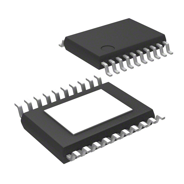


 工商网监
湘ICP备2023018690号
工商网监
湘ICP备2023018690号
