LTC1258CMS8#PBF

LTC1258CMS8#PBF

  • 厂商:

    AD(亚德诺)

  • 封装:

    TSSOP8

  • 描述:

    IC VREF SERIES ADJ 0.46% 8MSOP

  • 详情介绍
  • 数据手册
  • 价格&库存
LTC1258CMS8#PBF 数据手册
LTC1258 Series Micropower Low Dropout References FEATURES DESCRIPTION n The LTC®1258/LTC1258-2.5/LTC1258-3/LTC1258-4.1/ LTC1258-5 are micropower bandgap references that combine high accuracy and low drift with very low supply current and small package size. The combination of ultralow quiescent current and low dropout voltage of only 200mV maximum makes them ideal for battery-powered equipment. The output voltage is set by an external resistor divider for the adjustable LTC1258. n n n n n n n 200mV Max Dropout at 10mA Output Current 4μA Typical Quiescent Current 0.15% Max Initial Accuracy (S8) No Output Capacitor Required Output Sources 10mA, Sinks 2mA 40ppm/°C Max Drift (S8) Voltage Options: 2.5V, 3V, 4.1V, 5V and Adjustable Available in Small MSOP Package This series of references uses curvature compensation to obtain low temperature coefficient and trimmed thin-film resistors to achieve high output accuracy. These references can source up to 10mA and sink up to 2mA, making them ideal for precision regulator applications. They are stable without an output bypass capacitor, but are also stable with capacitance up to 1μF. This feature is important in critical applications where PC board space is a premium and fast settling is demanded. APPLICATIONS n n n n Battery-Powered Systems Handheld Instruments Precision Power Supplies A/D and D/A Converters The LTC1258 series references provide power dissipation advantages over shunt references. In addition to supply current, shunt references must also idle the entire load current to operate. The LTC1258 series is available in the 8-pin MSOP and SO packages. L, LT, LTC and LTM are registered trademarks of Linear Technology Corporation. All other trademarks are the property of their respective owners. TYPICAL APPLICATION LTC1258-2.5 Temperature Drift 2.5V Battery-Powered Reference LTC1258-2.5 2.7V TO 12.6V 2 IN OUT 1 0.1μF GND 4 1258 TA01 2.5V REFERENCE VOLTAGE CHANGE (mV) 4 3 2 1 0 –1 –2 –3 –4 –40 –20 0 20 40 60 TEMPERATURE (°C) 80 100 1258 TA02 1258sfb 1 LTC1258 Series ABSOLUTE MAXIMUM RATINGS (Note 1) Supply Voltage ..........................................................13V Input Voltages ............................................ –0.3V to 13V Output Voltages ......................................... –0.3V to 13V Output Short-Circuit Duration .......................... Indefinite Operating Temperature Range (Note 2).. –40°C to 100°C Specified Temperature Range ..................... 0°C to 70°C Storage Temperature Range (Note 3)..... –65°C to 150°C Lead Temperature (Soldering, 10 sec) .................. 300°C PIN CONFIGURATION TOP VIEW TOP VIEW OUT IN **DNC/FB GND 1 2 3 4 8 7 6 5 DNC* DNC* DNC* DNC* MS8 PACKAGE 8-LEAD PLASTIC MSOP OUT 1 8 DNC* IN 2 7 DNC* **DNC/FB 3 6 DNC* GND 4 5 DNC* S8 PACKAGE 8-LEAD PLASTIC SO TJMAX = 125°C, θJA = 250°C/W *CONNECTED INTERNALLY. DO NOT CONNECT EXTERNAL CIRCUITRY TO THESE PINS **DNC FOR LTC1258-2.5/LTC1258-3/LTC1258-4.1/LTC1258-5, FB FOR LTC1258 TJMAX = 125°C, θJA = 190°C/W *CONNECTED INTERNALLY. DO NOT CONNECT EXTERNAL CIRCUITRY TO THESE PINS **DNC FOR LTC1258-2.5/LTC1258-3/LTC1258-4.1/LTC1258-5, FB FOR LTC1258 ORDER INFORMATION LEAD FREE FINISH TAPE AND REEL PART MARKING PACKAGE DESCRIPTION TEMPERATURE RANGE LTC1258CMS8#PBF (OBSOLETE) LTC1258CMS8#TRPBF LTEL 8-Lead Plastic MSOP 0°C to 70°C LTC1258CMS8-2.5#PBF LTC1258CMS8-2.5#TRPBF LTCF 8-Lead Plastic MSOP 0°C to 70°C LTC1258CMS8-3#PBF LTC1258CMS8-3#TRPBF LTEU 8-Lead Plastic MSOP 0°C to 70°C LTC1258CMS8-4.1#PBF LTC1258CMS8-4.1#TRPBF LTEN 8-Lead Plastic MSOP 0°C to 70°C LTC1258CMS8-5#PBF LTC1258CMS8-5#TRPBF LTEM 8-Lead Plastic MSOP 0°C to 70°C LTC1258CS8#PBF (OBSOLETE) LTC1258CS8#TRPBF 1258 8-Lead Plastic SO 0°C to 70°C LTC1258CS8-2.5#PBF LTC1258CS8-2.5#TRPBF 12582 8-Lead Plastic SO 0°C to 70°C LTC1258CS8-3#PBF LTC1258CS8-3#TRPBF 12583 8-Lead Plastic SO 0°C to 70°C LTC1258CS8-4.1#PBF LTC1258CS8-4.1#TRPBF 125841 8-Lead Plastic SO 0°C to 70°C LTC1258CS8-5#PBF LTC1258CS8-5#TRPBF 12585 8-Lead Plastic SO 0°C to 70°C Consult LTC Marketing for parts specified with wider operating temperature ranges. Consult LTC Marketing for information on non-standard lead based finish parts. For more information on lead free part marking, go to: http://www.linear.com/leadfree/ For more information on tape and reel specifications, go to: http://www.linear.com/tapeandreel/ 1258sfb 2 LTC1258 Series AVAILABLE OPTIONS OUTPUT VOLTAGE (V) 2.5 2.5 3 3 4.096 4.096 5 5 TEMPERATURE RANGE (°C) 0 to 70 0 to 70 0 to 70 0 to 70 0 to 70 0 to 70 0 to 70 0 to 70 ACCURACY (%) 0.15 0.21 0.15 0.20 0.15 0.18 0.15 0.18 Adjustable Adjustable 0 to 70 0 to 70 0.4 0.46 PACKAGE TYPE TEMPERATURE SO-8 (S8) MSOP-8 (MS8) COEFFICENT (ppm/°C) ORDER NUMBER PART MARKING ORDER NUMBER PART MARKING 40 LTC1258CS8-2.5 12582 60 LTC1258CMS8-2.5 LTCF 40 LTC1258CS8-3 12583 60 LTC1258CMS8-3 LTEU 40 LTC1258CS8-4.1 125841 60 LTC1258CMS8-4.1 LTEN 40 LTC1258CS8-5 12585 60 LTC1258CMS8-5 LTEM OBSOLETE 40 LTC1258CS8 1258 60 LTC1258CMS8 LTEL ELECTRICAL CHARACTERISTICS The l denotes the specifications which apply over the full operating temperature range, otherwise specifications are at TA = 25°C. VIN = VOUT(NOMINAL) + 0.2V, IOUT = 0mA, FB = OUT for the LTC1258 unless otherwise noted. SYMBOL PARAMETER CONDITIONS MIN VIN Input Voltage Range IIN Input Current FB = OUT for LTC1258 VOUT Output Voltage (Note 4) en Output Voltage Noise (Note 5) LTC1258 (S8), FB = OUT LTC1258-2.5 (S8) LTC1258-3 (S8) LTC1258-4.1 (S8) LTC1258-5 (S8) LTC1258 (MS8), FB = OUT LTC1258-2.5 (MS8) LTC1258-3 (MS8) LTC1258-4.1 (MS8) LTC1258-5 (MS8) 0.1Hz ≤ f ≤ 10Hz TC Output Voltage Temp Coefficient (Note 6) VOUT/VIN Line Regulation VOUT/IOUT Load Regulation (Note 7) TYP l 4 l 2.3755 2.4963 2.9955 4.090 4.9925 2.374 2.4948 2.994 4.0885 4.991 2.385 2.5 3 4.096 5 2.385 2.5 3 4.096 5 8 MAX UNITS 12.6 V 6.5 8.5 2.3945 2.5037 3.0045 4.102 5.0075 2.396 2.5052 3.006 4.1035 5.009 μA μA V V V V V V V V V V ppmP-P TMIN ≤ TJ ≤ TMAX (S8) TMIN ≤ TJ ≤ TMAX (MS8) VIN = (VOUT(NOMINAL) + 0.2V) to 12.6V l l 15 l 30 40 60 120 Sourcing 0mA to 10mA l 0.1 0.3 mV/mA 1.75 4.0 6.5 mV/mA mV/mA mA mA mV mV Sinking 0mA to 2mA ISC Short-Circuit Output Current VOUT Shorted to GND VOUT Shorted to VIN ΔVDO Dropout Voltage (Note 8) IOUT = 0, ΔVOUT ≤ 0.1% IOUT = 10mA, ΔVOUT ≤ 0.1% VHYST Output Hysteresis (Note 9) IFB FB Pin Input Current ΔT = –40°C to 85°C ΔT = 0°C to 70°C LTC1258, OUT = FB Note 1: Stresses beyond those listed under Absolute Maximum Ratings may cause permanent damage to the device. Exposure to any Absolute Maximum Rating condition for extended periods may affect device reliability and lifetime. l 20 2 40 4 l l 100 200 ppm/°C ppm/°C ppm/V 200 50 ppm ppm 10 nA Note 2: The LTC1258 is guaranteed functional over the operating temperature range of –40°C to 100°C. Note 3: If the part is stored outside of the specified operating temperature range, the output may shift due to hysteresis. 1258sfb 3 LTC1258 Series ELECTRICAL CHARACTERISTICS Note 4: ESD (electrostatic discharge) sensitive device. Extensive use of ESD protection devices are used internal to the LTC1258, however, high electrostatic discharge can damage or degrade the device. Use proper ESD handling precautions. Note 5: Peak-to-peak noise is measured with a single pole highpass filter at 0.1Hz and 2-pole lowpass filter at 10Hz. Note 6: Temperature coefficient is the change in output voltage divided by the nominal output voltage divided by the specified temperature range. Note 7: Load regulation is measured on a pulse basis from no load to the specified load current. Output changes due to die temperature change must be taken into account separately. Note 8: Dropout voltage is (VIN – VOUT) when VOUT falls to 0.1% below its nominal value at VIN = VOUT + 0.5V. Note 9: Hysteresis in output voltage is created by package stress that differs depending on whether the IC was previously at a higher or lower temperature. Output voltage is always measured at 25°C, but the IC is cycled hot or cold before successive measurements. Hysteresis is not normally a problem for operational temperature excursions where the instrument might be stored at high or low temperature. TYPICAL PERFORMANCE CHARACTERISTICS LTC1258-2.5* Dropout Voltage vs Output Source Current LTC1258-2.5* Input Current vs Temperature 100 OUTPUT SHORT-CIRCUIT CURRENT (mA) VIN = 2.7V 7 80 INPUT CURRENT (μA) DROPOUT VOLTAGE (mV) 70 8 TA = 25oC 90 70 60 50 40 30 5 4 3 1 10 0 6 2 20 0 1 10 0.1 OUTPUT SOURCE CURRENT (mA) 0 –50 –25 100 0 20 10 5 0 5 0 25 50 75 100 125 150 TEMPERATURE (°C) TA = 25°C VIN = VOUT(NOM) + 0.2V 4 TA = 25°C OUTPUT SHORTED TO GND 14 1258-G04 2 4 6 8 10 INPUT VOLTAGE (V) 3 SINKING 2 1 SOURCING 0 –1 –2 –3 –4 41 12 OUTPUT SHORTED TO VIN LTC1258 Series Load Regulation $VOUT FROM NO LOAD (mV) 10 6 8 10 INPUT VOLTAGE (V) 30 5 OUTPUT SHORT-CIRCUIT CURRENT (mA) 15 4 40 1258 G03 42 2 50 LTC1258-2.5* Output ShortCircuit Current vs Input Voltage 25 20 OUTPUT SHORTED TO GND 1258 G02 LTC1258-2.5* Output ShortCircuit vs Input Voltage TA = 25°C OUTPUT SHORTED TO VIN TA = 25°C VIN = VOUT(NOM) + 0.2V 60 0 –50 –25 25 50 75 100 125 150 TEMPERATURE (°C) 1258 G01 OUTPUT SHORT-CIRCUIT CURRENT (mA) LTC1258 Series Output ShortCircuit Current vs Temperature 12 14 1258-G05 –5 0 1 10 0.1 OUTPUT CURRENT (mA) 100 1258 G06 *Similar performance characteristics can be expected for all voltage options. 1258sfb 4 LTC1258 Series TYPICAL PERFORMANCE CHARACTERISTICS LTC1258-2.5 Output Voltage vs Input Voltage LTC1258-2.5 Input Current vs Input Voltage 2.5010 60 2.5005 2.5000 2 4 6 8 10 INPUT VOLTAGE (V) 12 6 5 4 14 POWER SUPPLY REJECTION RATIO (dB) TA = 25°C INPUT CURRENT (μA) OUTPUT VOLTAGE (V) TA = 25°C 2.4995 LTC1258-2.5 PSRR vs Frequency 7 2 6 8 10 INPUT VOLTAGE (V) 4 12 1258 G07 40 30 20 10 0 14 100 1k FREQUENCY (Hz) 10 10k 1258 G09 1258 G08 LTC1258-5 Input Current vs Input Voltage in Dropout LTC1258-2.5 0.1Hz to 10Hz Noise LTC1258-2.5 Input Current vs Input Voltage in Dropout 1400 250 VIN = 2.7V TA = –55°C 1200 200 1000 INPUT CURRENT (μA) INPUT CURRENT (μA) TA = 25°C 5μV/DIV VIN = 2.7V 50 TA = 125°C 800 600 400 TA = 125°C TA = 25°C 150 100 TA = –55°C 50 200 0 0 1SEC/DIV 0 1258 G10 1 2 3 4 5 6 7 INPUT VOLTAGE (V) 8 9 10 0 0.5 1258 G11 1 1.5 2 2.5 3 3.5 INPUT VOLTAGE (V) 4 4.5 5 1258 G12 PIN FUNCTIONS OUT (Pin 1): Reference Output. The output can source up to 10mA and sink up to 2mA. It is stable with output bypass capacitor ranging from 0μF to 1μF. FB (Pin 3): (LT1258) Resistor Divider Feedback Pin. Connect a resistor divider from OUT to GND and the center tap to FB. This pin sets the output potential. IN (Pin 2): Positive Supply. Bypassing with a 0.1μF capacitor is recommended if the output loading changes. (VOUT + 0.2V) ≤ VIN ≤ 12.6V. ⎛ R1+ R2 ⎞ ; R1 is connected from OUT to VOUT = 2.385V ⎜ ⎝ R2 ⎟⎠ DNC (Pin 3): (LTC1258-2.5/LTC1258-3/LTC1258-4.1/ LTC1258-5) Do Not Connect. Connected internally for post package trim. This pin must be left unconnected. FB and R2 from FB to GND. GND (Pin 4): Negative Supply or Ground Connection. DNC (Pins 5, 6, 7, 8): Do Not Connect. Connected internally for post package trim. These pins must be left unconnected. 1258sfb 5 LTC1258 Series BLOCK DIAGRAM 2 IN + OUT 1 – 2.385V R1 FB 3 (LTC1258) R2 GND 4 1258 BD NOTE: R1 AND R2 ARE NOT CONNECTED FOR LTC1258 APPLICATIONS INFORMATION Longer Battery Life Output Bypass Capacitor Series references have an advantage over shunt style references. To operate, shunt references require a resistor between the power supply and the output. This resistor must be chosen to supply the maximum current that is demanded by the circuit being regulated. When the circuit being controlled is not operating at this maximum current, the shunt reference must always sink this current, resulting in high power dissipation and short battery life. The LTC1258 series is designed to be stable with or without capacitive loads. With no capacitive load, the reference is ideal for fast settling applications, or where PC board space is at a premium. The LTC1258 series low dropout references do not require a current setting resistor and can operate with any supply voltage from (VOUT(NOMINAL) + 0.2V) to 12.6V. When the circuitry being regulated does not demand current, the LTC1258 series reduces its dissipation and battery life is extended. If the reference is not delivering load current it dissipates only 10.8μW when operating on a 2.7V supply for LTC1258-2.5, yet the same connection can deliver 10mA of load current when demanded. In applications with significant output loading changes, an output bypass capacitor of up to 1μF can be used to improve the output transient response. Figure 1 shows the response of the reference to a 1mA to 0μA load step with a 1μF output capacitor. If more than 1μF of output capacitance is required, a resistor in series with the capacitor is recommended to reduce the output ringing. Figure 2 illustrates the use of a damping resistor for capacitive loads greater than 1μF. Figure 3 shows the resistor and capacitor values required to achieve critical damping. 1mA 1mA IOUT IOUT 0mA 0mA VOUT 100mV/DIV VOUT 100mV/DIV 10ms/DIV 1258 F01a 0.5ms/DIV 1258 F01b Figure 1. Reference Output Load Transient Response, 1μF Output Capacitor 1258sfb 6 LTC1258 Series APPLICATIONS INFORMATION 10k LTC1258-5 2 IN OUT GND 4 0.1μF 1 5V COUT >1μF DAMPING RESISTOR
LTC1258CMS8#PBF
物料型号:LTC1258系列,包括LTC1258、LTC1258-2.5、LTC1258-3、LTC1258-4.1、LTC1258-5以及可调版本。

器件简介:LTC1258系列是微功耗的带隙基准电压源,具有高准确度和低漂移,同时保持非常低的供电电流和小尺寸封装。这些基准电压源结合了超低的静态电流和仅200mV的最大降额电压,非常适合电池供电设备。

引脚分配: - OUT (Pin 1): 基准电压输出,可提供最大10mA的源电流和最大2mA的沉电流。 - IN (Pin 2): 正电源输入,建议在输出负载变化时使用0.1μF电容进行旁路。 - DNC (Pin 3): 不连接,对于LTC1258型号,此引脚内部连接用于封装后的修调。 - FB (Pin 3): 反馈引脚,对于可调版本,通过从OUT到GND的电阻分压器设置输出电压。 - GND (Pin 4): 负电源或地连接。 - DNC (Pins 5, 6, 7, 8): 不连接,内部用于封装后的修调。

参数特性: - 工作电压范围:2.2V至13V。 - 输出电压:固定版本有2.5V、3V、4.1V、5V,可调版本可通过外部电阻设置。 - 静态电流:典型值为4μA。 - 初始准确度:最大0.15%。 - 温度系数:最大40ppm/°C。 - 无需输出电容即可稳定工作,但也可以与高达1μF的电容一起使用。

功能详解:LTC1258系列基准电压源使用曲率补偿技术来获得低温度系数,并使用修调薄膜电阻来实现高输出准确度。它们可以在没有输出旁路电容的情况下稳定工作,但也可以与高达1μF的电容一起使用,这在PCB空间有限且需要快速稳定的场景中非常重要。

应用信息: - 电池供电系统 - 手持仪器 - 精密电源 - A/D和D/A转换器

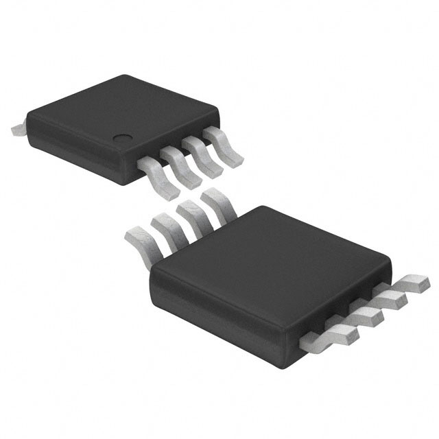
封装信息:LTC1258系列提供8引脚MSOP和SO封装。
LTC1258CMS8#PBF 价格&库存

很抱歉,暂时无法提供与“LTC1258CMS8#PBF”相匹配的价格&库存,您可以联系我们找货

免费人工找货