LTC1757A-1EMS8#TRPBF 数据手册
LTC1757A-1/LTC1757A-2
Single/Dual Band
RF Power Controllers
U
FEATURES
■
■
■
■
■
■
■
■
■
■
■
■
■
■
■
DESCRIPTIO
Dual Band RF Power Amplifier Control (LTC1757A-2)
Improved Internal Schottky Diode Detector
Wide Input Frequency Range: 850MHz to 2GHz
Autozero Cancels Initial Offsets and Temperature
Dependent Offset Errors
Wide VIN Range of 2.7V to 6V Allows
Direct Connection to Battery
RF Output Power Set by External DAC
Fast Acquire After Transmit Enable
Internal Frequency Compensation
Rail-to-Rail Power Control Outputs
RF PA Supply Current Limiting
Battery Overvoltage Protection
Power Control Signal Overvoltage Protection
Low Operating Current: 1mA
Very Low Shutdown Current: < 1µA
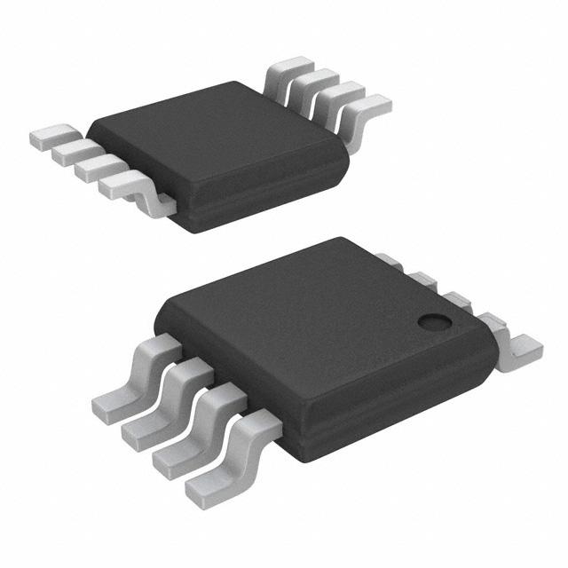
Available in a 8-Pin MSOP Package (LTC1757A-1)
and 10-Pin MSOP (LTC1757A-2)
U
APPLICATIO S
■
■
■
■
Single/Dual Band GSM Cellular Telephones
PCS Devices
Wireless Data Modems
TDMA Cellular Telephones
The LTC®1757A-2 is a dual band RF power controller for
RF power amplifiers operating in the 850MHz to 2GHz
range. The LTC1757A is pin compatible with the LTC1757
but has improved RF detection range. The input voltage
range is optimized for operation from a single lithium-ion
cell or 3× NiMH. Several functions required for RF power
control and protection are integrated in one small 10-pin
MSOP package, thereby minimizing PCB area.
The LTC1757A-1 is a single output RF power controller
that is identical in performance to the LTC1757A-2 except
that one output (VPCA) is provided. The LTC1757A-1 can
be used to drive a single RF channel or dual channel
module with integral multiplexer. This part is available in
an 8-pin MSOP package.
RF power is controlled by driving the RF amplifier power
control pins and sensing the resultant RF output power
via a directional coupler. The RF sense voltage is peak
detected using an on-chip Schottky diode. This detected
voltage is compared to the DAC voltage at the PCTL pin
to control the output power. The RF power amplifier is
protected against high supply voltage and current and
high power control pin voltages.
Internal and external offsets are cancelled over temperature by an autozero control loop, allowing accurate low
power programming. The shutdown feature disables the
part and reduces the supply current to < 1µA.
, LTC and LT are registered trademarks of Linear Technology Corporation.
U
TYPICAL APPLICATIO
LTC1757A-2 Dual Band Cellular Telephone Transmitter
68Ω
VIN
33pF
Li-Ion
SHDN
BSEL
LTC1757A-2
1
2
3
4
5
VIN
VCC
RF
VPCA
SHDN
VPCB
BSEL
TXEN
GND
PCTL
10
DIRECTIONAL
COUPLER
9
8
7
900MHz
DIPLEXER
RF PA
TXEN
6
50Ω
DAC
1.8GHz /1.9GHz
RF PA
1757A TA01
1
�LTC1757A-1/LTC1757A-2
W W
W
AXI U
U
ABSOLUTE
RATI GS
(Note 1)
VIN to GND ............................................... – 0.3V to 6.5V
VPCA, VPCB Voltage ..................................... – 0.3V to 3V
PCTL Voltage ............................... – 0.3V to (VIN + 0.3V)
RF Voltage ........................................ (VIN – 2.2V) to 7V
IVCC, Continuous ....................................................... 1A
IVCC, 12.5% Duty Cycle .......................................... 2.5A
SHDN, TXEN, BSEL
Voltage to GND ............................ – 0.3V to (VIN + 0.3V)
IVPCA/B, 25% Duty Cycle ...................................... 20mA
Operating Temperature Range
(Note 2) ................................................. – 30°C to 85°C
Storage Temperature Range ................ – 65°C to 150°C
Maximum Junction Temperature ........................ 125°C
Lead Temperature (Soldering, 10 sec)................ 300°C
U
U
W
PACKAGE/ORDER I FOR ATIO
ORDER PART
NUMBER
TOP VIEW
VIN
RF
SHDN
GND
1
2
3
4
8
7
6
5
VCC
VPCA
TXEN
PCTL
LTC1757A-1EMS8
ORDER PART
NUMBER
TOP VIEW
VIN
RF
SHDN
BSEL
GND
1
2
3
4
5
10
9
8
7
6
VCC
VPCA
VPCB
TXEN
PCTL
LTC1757A-2EMS
MS8 PACKAGE
8-LEAD PLASTIC MSOP
MS8 PART MARKING
MS10 PACKAGE
10-LEAD PLASTIC MSOP
MS10 PART MARKING
TJMAX = 150°C, θJA = 250°C/W
LTPL
TJMAX = 125°C, θJA = 250°C/W
LTPM
Consult factory for Industrial and Military grade parts.
ELECTRICAL CHARACTERISTICS
The ● denotes specifications which apply over the full operating
temperature range, otherwise specifications are at TA = 25°C. VIN = 3.6V, SHDN = TXEN = HI, unless otherwise noted.
PARAMETER
CONDITIONS
MIN
VIN Operating Voltage
(Note 7)
●
IVIN Shutdown Current
SHDN = LO, TXEN = LO, BSEL = LO
●
IVIN Autozero Current
SHDN = HI, TXEN = LO
●
IVIN Operating Current
SHDN = HI, TXEN = HI, IVPCA = IVPCB = 0mA, VPCA/B = HI
●
TYP
2.7
IVCC Current Limit
MAX
UNITS
6
V
1
µA
0.9
1.5
mA
1
1.6
mA
150
mΩ
0.1
V
VIN – 0.28
V
2.2
90
A
VIN to VCC Resistance
SHDN = LO, TXEN = LO
VPCA/B VOL
TXEN = HI, Open Loop, PCTL = – 100mV
●
VPCA/B Dropout Voltage
ILOAD = 5.5mA, VIN = 2.7V
●
VPCA/B Voltage Clamp
RLOAD = 400Ω
●
2.7
2.85
VPCA/B Output Current
VPCA/B = 2.4V, VIN = 2.7V
●
5.5
9
mA
VPCA/B Enable Time
VPCTL = 2V Step, CLOAD = 100pF (Note 5)
200
ns
VPCA/B Bandwidth
CLOAD = 100pF, RLOAD = 400Ω (Note 9)
VPCA/B Load Capacitance
(Note 6)
VPCA/B Slew Rate
VPCTL = 2V Step, CLOAD = 100pF (Note 3)
VPCA/B Droop
VIN = 2.7V, VPCTL = 2V Step
●
0
250
1.5
400
3.0
550
kHz
100
pF
3
V/µs
±10
550
µV/ms
VPCA/B TXEN Start Voltage
Open Loop, TXEN Low to High, CLOAD = 100pF (Note 10)
700
mV
SHDN Input Threshold
VIN = 2.7V to 6V, TXEN = LO
●
0.35
1.4
V
TXEN, BSEL Input Threshold
VIN = 2.7V to 4.7V
●
0.35
1.4
V
2
400
V
�LTC1757A-1/LTC1757A-2
ELECTRICAL CHARACTERISTICS
The ● denotes specifications which apply over the full operating
temperature range, otherwise specifications are at TA = 25°C. VIN = 3.6V, SHDN = TXEN = HI, unless otherwise noted.
PARAMETER
CONDITIONS
MIN
TYP
MAX
SHDN, TXEN, BSEL Input Current
SHDN, TXEN or BSEL = 3.6V
●
10
30
50
µA
PCTL Input Voltage Control Range
VIN = 2.7V to 4.7V, RLOAD = 400Ω
●
0
2
V
PCTL Input Voltage Range
VIN = 3V, RLOAD = 400Ω (Note 8)
●
PCTL Input Resistance
SHDN = LO, TXEN = LO
●
VIN = 2.7V, RLOAD = 400Ω (Note 4)
●
Autozero Settling Time (tS)
Shutdown to Enable (Autozero), VIN = 2.7V (Note 11)
●
RF Input Frequency Range
(Note 6)
●
RF Input Power Range
900MHz (Note 6)
1800MHz (Note 6)
50
PCTL Input Filter
Autozero Range
100
UNITS
2.4
V
150
kΩ
1.25
MHz
400
50
mV
µs
850
2000
MHz
– 24
–22
16
16
dBm
dBm
RF DC Input Resistance
Referenced to VIN, SHDN = LO, TXEN = LO
●
100
185
300
Ω
VIN Overvoltage Range
VPCA/B < 0.5V, RLOAD = 400Ω
●
4.8
5.0
5.4
V
BSEL Timing
t1, Setup Time Prior to TXEN Asserted High
t2, Hold Time After TXEN is Asserted Low
Note 1: Absolute Maximum Ratings are those values beyond which the life of
a device may be impaired.
Note 2: The LTC1757A-1 and LTC1757A-2 are guaranteed to meet performance
specifications from 0°C to 70°C. Specifications over the – 30°C to 85°C
operating temperature range are assured by design, characterization and
correlation with statistical process controls.
Note 3: Slew rate is measured open loop. The slew time at VPCA or VPCB is
measured between 1V and 2V.
Note 4: Maximum DAC zero-scale offset voltage that can be applied to PCTL.
Note 5: This is the time from TXEN rising edge 50% switch point to
VPCA/B = 1V.
200
200
ns
ns
Note 6: Guaranteed by design. This parameter is not production tested.
Note 7: For VIN voltages greater than 4.7V, VPCA/VPCB are set low by the
overvoltage shutdown.
Note 8: Includes maximum DAC offset voltage and maximum control voltage.
Note 9: Bandwidth is calculated using the 10% to 90% rise time equation:
BW = 0.35/rise time
Note 10: Measured 1µs after TXEN = HI.
Note 11: 50% switch point, SHDN HI = VIN, TXEN HI = VIN.
3
�LTC1757A-1/LTC1757A-2
U W
RF Detector Characteristics
at 900MHz
10000
VIN = 3V TO 4.4V
1000
100
10
–30°C
75°C
25°C
1
–24 –20 –16 –12 –8 –4 0 4 8
RF INPUT POWER (dBm)
12 16
1757A G01
U
U
U
PI FU CTIO S
PCTL REFERENCED DETECTOR OUTPUT VOLTAGE (mV)
PCTL REFERENCED DETECTOR OUTPUT VOLTAGE (mV)
TYPICAL PERFOR A CE CHARACTERISTICS
RF Detector Characteristics
at 1800MHz
10000
VIN = 3V TO 4.4V
1000
100
10
–30°C
75°C
25°C
1
–22 –18 –14 –10 –6 –2 2 6
RF INPUT POWER (dBm)
10 14
1757A G02
(LTC1757A-2/LTC1757A-1)
VIN (Pin 1): Input Supply Voltage, 2.7V to 6V. VIN should
be bypassed with 0.1µF and 100pF ceramic capacitors.
Used as return for RF 185Ω termination.
TXEN (Pin 7/Pin 6): Transmit Enable Input. A logic high
enables the control amplifier. When TXEN is low and
SHDN is high the part is in the autozero mode. This input
has an internal 150k resistor to ground.
RF (Pin 2): RF Feedback Voltage from the Directional
Coupler. Referenced to VIN. A coupling capacitor of 33pF
must be used to connect to the ground referenced directional coupler. The frequency range is 850MHz to 2000MHz.
This pin has an internal 185Ω termination, an internal
Schottky diode detector and peak detector capacitor.
VPCB (Pin 8): (LTC1757A-2 Only) Power Control Voltage
Output. This pin drives an external RF power amplifier
power control pin. The maximum load capacitance is
100pF. The output is capable of rail-to-rail swings at low
load currents. Selected when BSEL is high.
SHDN (Pin 3): Shutdown Input. A logic low on the SHDN
pin places the part in shutdown mode. A logic high places
the part in autozero when TXEN is low. SHDN has an internal 150k pull-down resistor to ensure that the part is in shutdown when the drivers are in a three-state condition.
VPCA (Pin 9/Pin 7): Power Control Voltage Output. This pin
drives an external RF power amplifier power control pin.
The maximum load capacitance is 100pF. The output is
capable of rail-to-rail swings at low load currents. Selected
when BSEL is low (LTC1757A-2 only).
BSEL (Pin 4): (LTC1757A-2 Only) Selects VPCA when low
and VPCB when high. This input has an internal 150k
resistor to ground.
VCC (Pin 10/Pin 8): RF Power Amplifier Supply. This pin
has an internal 0.050Ω sense resistor between VIN and
VCC that senses the RF power amplifier supply current to
detect overcurrent conditions.
GND (Pin 5/Pin 4): System Ground.
PCTL (Pin 6/Pin 5): Analog Input. The external power
control DAC drives this input. The amplifier servos the RF
power until the RF detected signal equals the DAC signal.
The input resistance is typically 100k.
4
�LTC1757A-1/LTC1757A-2
W
BLOCK DIAGRA
(LTC1757A-2)
DIPLEXER
900MHz
RF PA
RF PA
1.8GHz
50Ω
Li-Ion
10
1
VCC
VIN
RSENSE
0.05Ω
METAL
0.02Ω
0.02Ω
TXENB
100Ω
METAL
68Ω
AUTOZERO
–
PA
AZ
OVERCURRENT
–
VPCA
+
+
–
CS
9
ADJ
+
33pF
OFFSET
TRIM
2
RF
185Ω
+
gm
GAIN
TRIM
VIN
–+
600mV
PB
CAMP
50mV
VPCB
–
CC
ICL
42k
22pF
42k
60µA
5
8
6pF
400µA
140k
+
VPC
33k
RFDET
gm
–
16.7k
60µA
110k
33k
1.2V
GND
OVP
gm
173k
VIN
1.2V
BG1
1.2V BANDGAP
33k
600mV
54.5k
12Ω
BG1
THERMAL
SHUTDOWN
TSDB
PB
TSDB
OPERATE SHDN
TXENI
XMT AUTOZERO
150k
150k
3
SHDN
7
TXEN
MUX
CONTROL
150k
6
PCTL
12Ω
PA
4
100Ω
100Ω
BSEL
1757A BD
5
�LTC1757A-1/LTC1757A-2
U
W
U U
APPLICATIO S I FOR ATIO
Operation
The LTC1757A-2 dual band RF power control amplifier
integrates several functions to provide RF power control
over two frequencies ranging from 850MHz to 2GHz. The
device also prevents damage to the RF power amplifier
due to overvoltage or overcurrent conditions. These functions include an internally compensated power control
amplifier to control the RF output power, an autozero
section to cancel internal and external voltage offsets, a
sense amplifier with an internal sense resistor to limit the
maximum RF power amplifier current, an RF Schottky
diode peak detector and amplifier to convert the RF feedback signal to DC, a VPCA/B overvoltage clamp, a VIN
overvoltage detector, a bandgap reference, a thermal
shutdown circuit and a multiplexer to switch the control
amplifier output to either VPCA or VPCB.
Band Selection
The LTC1757A-2 is designed for dual band operation. The
BSEL pin will select output VPCA when low and output VPCB
when high. For example, VPCA could be used to drive a
900MHz channel and VPCB a 1.8GHz/1.9GHz channel.
BSEL must be established before the part is enabled. The
LTC1757A-1 can be used to drive a single RF channel or
dual channel module with integral multiplexer.
Control Amplifier
The control amplifier supplies the power control voltage to
the RF power amplifier. A portion (typically – 19dB for low
frequencies and –14dB for high frequencies) of the RF
output signal is sampled, via a directional coupler, to close
the gain control loop. When a DAC signal is applied to
PCTL, the amplifier quickly servos VPCA or VPCB positive
until the detected feedback voltage applied to the RF pin
matches the voltage at PCTL. This feedback loop provides
accurate RF power control. VPCA or VPCB are capable of
driving a 5.5mA load current and 100pF load capacitor.
RF Detector
The internal RF Schottky diode peak detector and amplifier converts the RF feedback voltage from the directional
coupler to a low frequency voltage. This voltage is compared to the DAC voltage at the PCTL pin by the control
6
amplifier to close the RF power control loop. The RF pin
input resistance is typically 185Ω and the frequency
range of this pin is 850MHz to 2000MHz. The detector
demonstrates excellent efficiency and linearity over a
wide range of input power. The Schottky detector is biased
at about 60µA and drives an on-chip peak detector capacitor of 22pF.
Autozero
An autozero system is included to improve power programming accuracy over temperature. This section cancels internal offsets associated with the Schottky diode
detector and control amplifier. External offsets associated
with the DAC driving the PCTL pin are also cancelled.
Offset drift due to temperature is cancelled between each
burst by the autozero system. The maximum offset allowed at the DAC output is limited to 400mV. Autozeroing
is performed when the part is in autozero mode (SHDN =
high, TXEN = low). When the part is enabled (TXEN = high,
SHDN = high) the autozero capacitors are held and the
VPCA or VPCB pin is connected to the control amplifier
output. The hold droop voltage of typically 10µV/ms
provides for accurate offset cancellation over the 1/8 duty
cycle associated with the GSM protocol as well as multislot
protocals. The part must be in the autozero mode for at
least 50µs for autozero to settle to the correct value.
Protection Features
The RF power amplifier is overcurrent protected by an
internal sense amplifier. The sense amplifier measures the
voltage across an internal 0.050Ω resistor to determine
the RF power amplifier current. VPCA or VPCB is lowered as
this supply current exceeds 2.2A, thereby regulating the
current to about 2.25A. The regulated current limit is
temperature compensated. The 0.050Ω resistor and the
current limit feature can be removed by connecting the PA
directly to VIN.
The RF power amplifier control voltage pins are overvoltage protected. The VPC overvoltage clamp regulates VPCA
or VPCB to 2.85V when the gain and PCTL input combination attempts to exceed this voltage.
The RF power amplifier is protected against excessive
input supply voltages. The VIN overvoltage detector starts
�LTC1757A-1/LTC1757A-2
U
W
U U
APPLICATIO S I FOR ATIO
to reduce VPCA or VPCB when VIN exceeds 5V. VPCA or VPCB
will be reduced to 0V as VIN continues to increase by about
200mV. This gain control voltage reduction lowers the RF
output power eventually reducing it to zero.
The internal thermal shutdown circuit will disable the
LTC1757A-2 if the junction temperature exceeds approximately 150°C. The part will be enabled when the temperature falls below 140°C.
Modes of Operation
The LTC1757A-2 supports three operating modes: shutdown, autozero and enable.
In shutdown mode (SHDN = Low) the part is disabled and
supply currents will be reduced to


 工商网监
湘ICP备2023018690号
工商网监
湘ICP备2023018690号
