LTC1758-1/LTC1758-2
RF Power Controllers with
250kHz Control Loop Bandwidth and
40dB Dynamic Range
DESCRIPTIO
U
FEATURES
■
■
■
■
■
■
■
■
■
■
■
■
■
■
■
■
■
Dual Band RF Power Amplifier Control (LTC1758-2)
Internal Schottky Diode Detector with Improved
Dynamic Range vs LTC1757A
Wide Input Frequency Range: 850MHz to 2GHz
Autozero Loop Cancels Offset Errors and
Temperature Dependent Offsets
Wide VIN Range: 2.7V to 6V
Allows Direct Connection to Battery
RF Output Power Set by External DAC
250kHz Control Loop Bandwidth
Fast Acquire After Transmit Enable
Internal Frequency Compensation
Rail-to-Rail Power Control Outputs
Power Control Signal Overvoltage Protection
Low Operating Current: 1mA
Very Low Shutdown Current: < 1µA
Available in 8-Pin MSOP (LTC1758-1)
and 10-Pin MSOP (LTC1758-2) Packages
Pin Compatible with LTC1757A-X
Improved Start Voltage Accuracy
Improved PCTL Input Filtering
U
APPLICATIO S
■
■
■
Single and Dual Band GSM/GPRS Cellular Telephones
PCS Devices
Wireless Data Modems
U.S. TDMA Cellular Phones
The LTC1758-1 is a single output RF power controller
that is identical in performance to the LTC1758-2 except
that one output (VPCA) is provided. The LTC1758-1 can
be used to drive a single RF or dual channel module with
integral multiplexer. This part is available in an 8-pin
MSOP package.
RF power is controlled by driving the RF amplifier power
control pins and sensing the resultant RF output power
via a directional coupler. The RF sense voltage is peak
detected using an on-chip Schottky diode. This detected
voltage is compared to the DAC voltage at the PCTL pin
to control the output power. The RF power amplifier is
protected against high supply current and high power
control pin voltages.
Internal and external offsets are cancelled over temperature by an autozero control loop, allowing accurate low
power programming. The shutdown feature disables the
part and reduces the supply current to < 1µA.
, LTC and LT are registered trademarks of Linear Technology Corporation.
U
■
The LTC®1758-2 is a dual band RF power controller for
RF power amplifiers operating in the 850MHz to 2GHz
range. The loop bandwidth reduction to 250kHz improves frequency stability when controlling slow turn-on
PAs such as the Philips BGY280, Conexant RM009/
CX77302, Anadigics AWT6102/AWT6107 and the Hitachi
PF08107/PF08123B.
TYPICAL APPLICATIO
LTC1758-2 Dual Band Cellular Telephone Transmitter
68Ω
VIN 33pF
LTC1758-2
1
2
Li-Ion
SHDN
BSEL
3
4
5
VIN
VCC
RF
VPCA
SHDN
VPCB
BSEL
TXEN
GND
PCTL
10
DIRECTIONAL
COUPLER
9
8
7
900MHz
DIPLEXER
RF PA
TXEN
6
50Ω
DAC
1.8GHz /1.9GHz
RF PA
1758 TA01
1
�LTC1758-1/LTC1758-2
W W
W
AXI U
U
ABSOLUTE
RATI GS
(Note 1)
VIN to GND ............................................... – 0.3V to 6.5V
VPCA, VPCB Voltage ..................................... – 0.3V to 3V
PCTL Voltage ............................... – 0.3V to (VIN + 0.3V)
RF Voltage ........................................ (VIN – 2.2V) to 7V
IVCC, Continuous ....................................................... 1A
IVCC, 12.5% Duty Cycle .......................................... 2.5A
SHDN, TXEN, BSEL
Voltage to GND ............................ – 0.3V to (VIN + 0.3V)
IVPCA/B, 25% Duty Cycle ...................................... 20mA
Operating Temperature Range (Note 2) . – 30°C to 85°C
Storage Temperature Range ................ – 65°C to 150°C
Maximum Junction Temperature ........................ 125°C
Lead Temperature (Soldering, 10 sec)................ 300°C
U
U
W
PACKAGE/ORDER I FOR ATIO
ORDER PART
NUMBER
TOP VIEW
VIN
RF
SHDN
GND
1
2
3
4
8
7
6
5
VCC
VPCA
TXEN
PCTL
LTC1758-1EMS8
MS8 PACKAGE
8-LEAD PLASTIC MSOP
TOP VIEW
VIN
RF
SHDN
BSEL
GND
MS8 PART MARKING
TJMAX = 125°C, θJA = 160°C/W
1
2
3
4
5
10
9
8
7
6
VCC
VPCA
VPCB
TXEN
PCTL
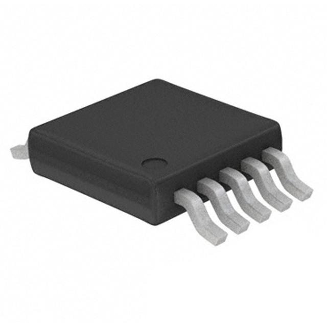
MS10 PACKAGE
10-LEAD PLASTIC MSOP
ORDER PART
NUMBER
LTC1758-2EMS
MS10 PART MARKING
TJMAX = 125°C, θJA = 160°C/W
LTSL
LTSM
Consult LTC Marketing for parts specified with wider operating temperature ranges.
ELECTRICAL CHARACTERISTICS
The ● denotes specifications which apply over the full operating
temperature range, otherwise specifications are at TA = 25°C. VIN = 3.6V, SHDN = TXEN = HI, unless otherwise noted.
PARAMETER
CONDITIONS
VIN Operating Voltage
IVIN Shutdown Current
MIN
●
SHDN = LO, TXEN = LO, BSEL = LO
●
IVIN Autozero Current
SHDN = HI, TXEN = LO
●
IVIN Operating Current
SHDN = HI, TXEN = HI, IVPCA = IVPCB = 0mA, VPCA/B = HI
TYP
2.7
IVCC Current Limit
MAX
UNITS
6
V
1
µA
1
1.6
mA
1.1
1.7
mA
2.2
A
VIN to VCC Resistance
SHDN = LO, TXEN = LO
VPCA/B VOL
TXEN = HI, Open Loop, PCTL = –100mV
●
VPCA/B Dropout Voltage
ILOAD = 5.5mA, VIN = 2.7V
●
VPCA/B Voltage Clamp
RLOAD = 400Ω, PCTL = 2V, External Gain = 0.417
●
2.7
2.85
VPCA/B Output Current
VPCA/B = 2.4V, VIN = 2.7V
VPCA/B = 2.6V, VIN = 3V
●
●
5.5
6
9
10
VPCA/B Enable Time
VPCTL = 2V Step, CLOAD = 100pF (Note 5)
●
620
1000
ns
VPCA/B Bandwidth
CLOAD = 100pF, RLOAD = 400Ω (Note 8)
●
180
250
330
kHz
●
0.75
1.3
500
600
VPCA/B Load Capacitance
(Note 6)
VPCA/B Slew Rate
VPCTL = 2V Step, CLOAD = 100pF (Note 3)
VPCA/B Droop
VIN = 2.7V, VPCTL = 2V Step
VPCA/B TXEN Start Voltage
Open Loop, TXEN Low to High, CLOAD = 100pF (Note 9)
SHDN Input Threshold
VIN = 2.7V to 6V, TXEN = LO
●
TXEN, BSEL Input Threshold
VIN = 2.7V to 6V
●
2
90
150
mΩ
0
0.1
V
VIN – 0.28
V
3.0
V
mA
mA
100
pF
V/µs
±1
µV/ms
700
mV
0.35
1.4
V
0.35
1.4
V
�LTC1758-1/LTC1758-2
ELECTRICAL CHARACTERISTICS
The ● denotes specifications which apply over the full operating
temperature range, otherwise specifications are at TA = 25°C. VIN = 3.6V, SHDN = TXEN = VIN, unless otherwise noted.
PARAMETER
CONDITIONS
MIN
TYP
MAX
SHDN, TXEN, BSEL Input Current
SHDN, TXEN or BSEL = 3.6V
●
10
25
50
µA
PCTL Input Voltage Control Range
VIN = 3V to 6V, RLOAD = 400Ω
●
0
2
V
PCTL Input Voltage Range
VIN = 3V, RLOAD = 400Ω (Note 7)
●
PCTL Input Resistance
SHDN = LO, TXEN = LO
●
VIN = 2.7V, RLOAD = 400Ω (Note 4)
●
Autozero Settling Time (tS)
tS, Shutdown to Enable (Autozero), VIN = 2.7V (Note 10)
●
RF Input Frequency Range
(Note 6)
●
RF Input Power Range
900MHz (Note 6)
1800MHz (Note 6)
50
PCTL Input Filter
90
UNITS
2.4
V
140
kΩ
350
Autozero Range
RF Input Impedance
Referenced to VIN, SHDN = LO, TXEN = LO
BSEL Timing
t1, Setup Time Prior to TXEN Asserted High
t2, Hold Time After TXEN is Asserted Low
Note 1: Absolute Maximum Ratings are those values beyond which the life
of a device may be impaired.
Note 2: The LTC1758-1 and LTC1758-2 are guaranteed to meet
performance specifications from 0°C to 70°C. Specifications over the
– 30°C to 85°C operating temperature range are assured by design,
characterization and correlation with statistical process controls.
Note 3: Slew rate is measured open loop. The slew time at VPCA or VPCB is
measured between 1V and 2V.
Note 4: Maximum DAC zero-scale offset voltage that can be applied to
PCTL.
●
kHz
400
mV
µs
50
850
2000
MHz
– 26
–24
16
16
dBm
dBm
100
200
Ω
350
200
200
ns
ns
Note 5: This is the time from TXEN rising edge 50% switch point to
VPCA/B = 1V.
Note 6: Guaranteed by design. This parameter is not production tested.
Note 7: Includes maximum DAC offset voltage and maximum control
voltage.
Note 8: Bandwidth is calculated using the 10% to 90% rise time:
BW = 0.35/rise time
Note 9: Measured 1µs after TXEN = HI.
Note 10: 50% switch point, SHDN HI = VIN, TXEN HI = VIN.
U W
RF Detector Characteristics
at 900MHz
10000
VIN = 3V TO 4.4V
1000
100
–30°C
10
75°C
25°C
1
–26
–20
–14 –8
–2
4
RF INPUT POWER (dBm)
10
16
1758 G01
PCTL REFERENCED DETECTOR OUTPUT VOLTAGE (mV)
PCTL REFERENCED DETECTOR OUTPUT VOLTAGE (mV)
TYPICAL PERFOR A CE CHARACTERISTICS
RF Detector Characteristics
at 1800MHz
10000
VIN = 3V TO 4.4V
1000
100
–30°C
10
25°C
75°C
1
–24 –20 –16 –12 –8 –4 0 4 8
RF INPUT POWER (dBm)
12 16
1758 G02
3
�LTC1758-1/LTC1758-2
U
U
U
PI FU CTIO S
(LTC1758-2/LTC1758-1)
VIN (Pin 1): Input Supply Voltage, 2.7V to 6V. VIN should
be bypassed with 0.1µF and 100pF ceramic capacitors.
Used as return for RF 200Ω termination.
RF (Pin 2): RF Feedback Voltage from the Directional
Coupler. Referenced to VIN. A coupling capacitor of 33pF
must be used to connect to the ground referenced directional coupler. The frequency range is 850MHz to 2000MHz.
This pin has an internal 200Ω termination, an internal
Schottky diode detector and peak detector capacitor.
SHDN (Pin 3): Shutdown Input. A logic low on the SHDN
pin places the part in shutdown mode. A logic high places
the part in autozero when TXEN is low. SHDN has an internal 150k pull-down resistor to ensure that the part is in shutdown when the drivers are in a three-state condition.
BSEL (Pin 4): (LTC1758-2 Only) Selects VPCA when low
and VPCB when high. This input has an internal 150k
resistor to ground.
GND (Pin 5/Pin 4): System Ground.
PCTL (Pin 6/Pin 5): Analog Input. The external power
control DAC drives this input. The amplifier servos the RF
4
power until the RF detected signal equals the DAC signal.
The input impedance is typically 90kΩ.
TXEN (Pin 7/Pin 6): Transmit Enable Input. A logic high
enables the control amplifier. When TXEN is low and
SHDN is high the part is in the autozero mode. This input
has an internal 150k resistor to ground.
VPCB (Pin 8): (LTC1758-2 Only) Power Control Voltage
Output. This pin drives an external RF power amplifier
power control pin. The maximum load capacitance is
100pF. The output is capable of rail-to-rail swings at low
load currents. Selected when BSEL is high.
VPCA (Pin 9/Pin 7): Power Control Voltage Output. This pin
drives an external RF power amplifier power control pin.
The maximum load capacitance is 100pF. The output is
capable of rail-to-rail swings at low load currents. Selected
when BSEL is low (LTC1758-2 only).
VCC (Pin 10/Pin 8): RF Power Amplifier Supply. This pin
has an internal 0.090Ω sense resistor between VIN and
VCC that senses the RF power amplifier supply current to
detect overcurrent conditions.
�LTC1758-1/LTC1758-2
W
BLOCK DIAGRA
(LTC1758-2)
DIPLEXER
900MHz
RF PA
RF PA
1.8GHz/1.9GHz
50Ω
Li-Ion
10
1
VCC
VIN
RSENSE
0.05Ω
METAL
0.02Ω
0.02Ω
TXENB
100Ω
METAL
68Ω
AUTOZERO
–
PA
AZ
OVERCURRENT
–
VPCA
+
ADJUSTABLE
9
CS
+
33pF
OFFSET
TRIM
2
RF
200Ω
+
gm
GAIN
TRIM
50mV
VIN
–+
PB
CAMP
FILTER
VPCB
–
8
PROGRAMMABLE
ICL
200Ω
CC
400µA
33k
35k
28pF
35k
140k
VPC
+
gm
RFDET
110k
–
22k
60µA
5
60µA
1.2V
GND
33k
COMPRESSION
1.2V
BG1
1.2V BANDGAP
22k
ADJUSTABLE
22k
12Ω
BG1
THERMAL
SHUTDOWN
TSDB
PB
TSDB
OPERATE SHDN
TXENI
XMT AUTOZERO
150k
150k
3
SHDN
7
TXEN
MUX
CONTROL
150k
6
PCTL
12Ω
PA
4
100Ω
100Ω
BSEL
1758 BD
5
�LTC1758-1/LTC1758-2
U
W
U
U
APPLICATIONS INFORMATION
Forward
Control Amplifier
The LTC1758 has a wider dynamic range than the
LTC1757A. The Schottky diode detector dynamic range
has been extended to over 40dB. The start voltage accuracy has been improved to ±17%. The autozero hold time
has been increased for applications requiring transmit
times of several hundred milliseconds. The PCTL input
filter bandwidth has been reduced to 350kHz for improved
rejection of DAC noise as well as smoother ramp shaping.
The bandwidth has been reduced to 250kHz to control
slow turn-on RF power amplifiers.
The control amplifier supplies the power control voltage to
the RF power amplifier. A portion (typically – 19dB for low
frequencies and –14dB for high frequencies) of the RF
output voltage is sampled, via a directional coupler, to
close the gain control loop. When a DAC voltage is applied
to PCTL, the amplifier quickly servos VPCA or VPCB positive
until the detected feedback voltage applied to the RF pin
matches the voltage at PCTL. This feedback loop provides
accurate RF power control. VPCA or VPCB are capable of
driving a 5.5mA load current and 100pF load capacitor.
Operation
RF Detector
The LTC1758-2 dual band RF power control amplifier
integrates several functions to provide RF power control
over frequencies ranging from 850MHz to 2GHz. The
device also prevents damage to the RF power amplifier
due to overvoltage or overcurrent conditions. These functions include an internally compensated power control,
amplifier to control the RF output power, an autozero
section to cancel internal and external voltage offsets, a
sense amplifier with an internal sense resistor to limit the
maximum RF power amplifier current, an RF Schottky
diode peak detector and amplifier to convert the RF feedback signal to DC, a VPCA/B overvoltage clamp, gain
compression, a bandgap reference, a thermal shutdown
circuit and a multiplexer to switch the control amplifier
output to either VPCA or VPCB.
The internal RF Schottky diode peak detector and amplifier converts the RF feedback voltage from the directional
coupler to a low frequency voltage. This voltage is compared to the DAC voltage at the PCTL pin by the control
amplifier to close the RF power control loop. The RF pin
input resistance is typically 200Ω and the frequency
range of this pin is 850MHz to 2000MHz. The detector
demonstrates excellent efficiency and linearity over a
wide range of input power. The Schottky detector is biased
at about 60µA and drives an on-chip peak detector capacitor of 28pF.
Band Selection
The LTC1758-2 is designed for dual band operation. The
BSEL pin will select output VPCA when low and output
VPCB when high. For example, VPCA could be used to drive
a 900MHz channel and VPCB a 1.8GHz/1.9GHz channel.
BSEL must be established before the part is enabled. The
LTC1758-1 can be used to drive a single RF channel or
dual channel with integral multiplexer.
6
Autozero
An autozero system is included to improve power programming accuracy over temperature. This section cancels internal offsets associated with the Schottky diode
detector and control amplifier. External offsets associated
with the DAC driving the PCTL pin are also cancelled.
Offset drift due to temperature is cancelled between each
burst. The maximum offset allowed at the DAC output is
limited to 400mV. Autozeroing is performed when the
part is in autozero mode (SHDN = high, TXEN = low).
When the part is enabled (TXEN = high, SHDN = high) the
autozero capacitors are held and the VPCA or VPCB pin is
connected to the control amplifier output. The hold droop
voltage of typically < 1µV/ms provides for accurate offset
cancellation over the normal 1/8 duty cycle associated
with the GSM protocol as well as with multislot protocols.
The part must be in the autozero mode for at least 50µs for
autozero to settle to the correct value.
�LTC1758-1/LTC1758-2
U
U
W
U
APPLICATIONS INFORMATION
Filter
Modes of Operation
There is a 350kHz single pole filter included in the PCTL
path.
The LTC1758-2 supports three operating modes: shutdown, autozero and enable.
Protection Features
In shutdown mode (SHDN = Low) the part is disabled and
supply currents will be reduced to 640mV. The external voltage
gain contributed by the RF power amplifier and directional
coupler network is 0.6 • ∆VPCTL/∆VVPCA and (1.18PCTL –
0.38V) • ∆VPCTL/∆VPCA. Measuring voltage gain in the
closed loop configuration accounts for the nonlinear detector gain that is dependent on RF input voltage and
frequency.
The LTC1758 unity gain bandwidth specified in the data
sheet assumes that the net voltage gain contributed by the
RF power amplifier and directional coupler is unity. The
bandwidth is calculated by measuring the rise time between 10% and 90% of the voltage change at VPCA or VPCB
for a small step in voltage applied to PCTL.
BW1 = 0.35/rise time
The LTC1758 control amplifier unity gain bandwidth (BW1)
is typically 250kHz. The phase margin of the control
amplifier is typically 90°.
RLOAD = 2k
CLOAD = 33pF
PHASE
GAIN
1k
10k
100k
FREQUENCY (Hz)
1M
140
130
120
110
100
90
80
70
60
50
40
30
20
10
0
10M
1758 F03
Figure 3. Measured Open Loop Gain and Phase, PCTL < 640mV
10
The phase margin degradation, due to external and internal pole combinations, is difficult to determine since
complex poles are present. Gain peaking may occur,
resulting in higher bandwidth and lower phase margin
than predicted from the open loop Bode plot. A low
frequency AC SPICE model of the LTC1758 power controller is included to better determine pole and zero interactions. The user can apply external gains and poles to
determine bandwidth and phase margin. DC, transient and
RF information cannot be extracted from the present
model. The model is suitable for external gain evaluations
up to 6×. The 350kHz PCTL input filter limits the bandwidth, therefore, use the RF input as demonstrated in the
model.
80
70
60
50
40
30
20
10
0
–10
–20
–30
–40
–50
–60
100
RLOAD = 2k
CLOAD = 33pF
PHASE
GAIN
1k
10k
100k
FREQUENCY (Hz)
1M
150
140
130
120
110
100
90
80
70
60
50
40
30
20
10
10M
PHASE (DEG)
80
70
60
50
40
30
20
10
0
–10
–20
–30
–40
–50
–60
100
PHASE (DEG)
VOLTAGE GAIN (dB)
For example, to determine the external RF channel loop
voltage gain with the loop closed, apply a 100mV step to
PCTL from 300mV to 400mV. VPCA (or VPCB) will increase
to supply enough feedback voltage to the RF pin to cancel
this 100mV step which would be the required detected
voltage of 60mV. VPCA changed from 1.498V to 1.540V to
create the RF output power change required. The net
external voltage gain contributed by the RF power amplifier and directional coupler network can be calculated by
dividing the 60mV change at the RF pin by the 42mV
change at the VPCA pin. The net external voltage gain would
then be approximately 1.4. The loop bandwidth extends to
1.4␣ • BW1. If BW1 is 250kHz, the loop bandwidth increases to approximately 350kHz. The phase margin is
extracted from Figure 3. Repeat the above voltage gain
measurement over the full power and frequency range.
VOLTAGE GAIN (dB)
Determining External Loop Gain and Bandwidth
1758 F04
Figure 4. Measured Open Loop Gain and Phase, PCTL > 640mV
�LTC1758-1/LTC1758-2
U
W
U U
APPLICATIO S I FOR ATIO
This model (Figure 7) is being supplied to LTC users as an
aid to circuit designs. While the model reflects close
similarity to corresponding devices in low frequency AC
performance terms, its use is not suggested as a replacement for breadboarding. Simulation should be used as a
forerunner or a supplement to traditional lab testing.
Users should note very carefully the following factors
regarding this model: Model performance in general will
reflect typical baseline specs for a given device, and
certain aspects of performance may not be modeled fully.
While reasonable care has been taken in the preparation,
we cannot be responsible for correct application on any
and all computer systems. Model users are hereby notified
that these models are supplied “as is”, with no direct or
implied responsibility on the part of LTC for their operation
within a customer circuit or system. Further, Linear Technology Corporation reserves the right to change these
models without prior notice.
Linear Technology Corporation hereby grants the users of
this model a nonexclusive, nontransferable license to use
this model under the following conditions:
The user agrees that this model is licensed from Linear
Technology and agrees that the model may be used,
loaned, given away or included in other model libraries as
long as this notice and the model in its entirety and
unchanged is included. No right to make derivative works
or modifications to the model is granted hereby. All such
rights are reserved.
This model is provided as is. Linear Technology makes no
warranty, either expressed or implied about the suitability
or fitness of this model for any particular purpose. In no
event will Linear Technology be liable for special, collateral, incidental or consequential damages in connection
with or arising out of the use of this model. It should be
remembered that models are a simplification of the actual
circuit.
CONTROL
AMPLIFER
BW1 ≅ 250kHz
RF POWER AMP
VPCA/B
G1
G2
+
PCTL
–
LTC1758
H1
RF
H2
1758 F05
RF DETECTOR
DIRECTIONAL
COUPLER
14dB to 20dB LOSS
Figure 5. Closed Loop Block Diagram
80
70
60
50
40
30
20
10
0
–10
–20
–30
–40
–50
–60
100
PHASE
RLOAD = 2k
CLOAD = 33pF
GAIN
1k
10k
100k
FREQUENCY (Hz)
1M
120
110
100
90
80
70
60
50
40
30
20
10
0
–10
–20
10M
PHASE (DEG)
IFB
CONTROLLED
RF OUTPUT
POWER
VOLTAGE GAIN (dB)
In all cases, the current data sheet information is your final
design guideline, and is the only performance guarantee.
For further technical information, refer to individual device
data sheets. Your feedback and suggestions on this model
is appreciated.
1758 F06
Figure 6. SPICE Model Open Loop Gain and Phase
Characteristics from RF to VPCA, PCTL < 640mV
11
�LTC1758-1/LTC1758-2
U
W
U U
APPLICATIO S I FOR ATIO
*LTC1758 Low Frequency AC Spice Model*
GIN1 ND2 0 ND1A IFB 100E-6
GX3 ND6 0 0 ND4 1E-6
GX4 ND7 0 0 ND6 1E-6
GX1 ND3 0 0 ND2 1E-6
GX2 ND4 0 0 ND3 1E-6
GX5 ND10 0 0 ND9 1E-6
GX8 ND14 0 0 ND12 1E-6
GX7 ND12 0 0 ND11 1E-6
GX6 ND11 0 0 ND10 1E-6
GXFB IFB 0 0 ND14 28.8E-6
EX1 ND8 0 0 ND7 1
RPCTL2 ND1 0 33E3
RFILT ND1 ND1A 50E3
RO1 ND2 0 70E6
RX3 ND6 0 1E6
RX4 ND7 0 1E6
RPCTL1 PCTL ND1 53E3
RX1 ND3 0 1E6
RX2 ND4 ND5 1E6
RSD RF ND9 500
RX5 ND10 0 1E6
RT RF 0 250
RX8 ND14 0 1E6
RX7 ND12 ND13 1E6
RX6 ND11 0 1E6
R9 ND8 ND8A 100
R9A ND8A VPCA 20
RLOAD VPCA 0 2E3
RFB1 IFB 0 22E3
CPCTL1 ND1A 0 7E-12
CX3 ND6 0 8E-15
CX4 ND7 0 12E-15
CC1 ND2 0 45E-12
CX1 ND3 0 2E-15
CX5 ND10 0 10E-15
CX6 ND11 0 1.2E-15
CLOAD VPCA 0 33E-12
CLINT ND8A 0 37E-12
CLINTA VPCA 0 18E-12
CFB1 IFB 0 300E-15
CP ND9 0 28E-12
LX2 ND5 0 34E-3
LX7 ND13 0 7E-3
**Closed loop connections, comment-out VPCTLO, VRF, Adjust EFB gain to reflect external gain, currently set at 3X**
*EFB RF 0 VPCA VIN 3
VIN VIN 0 DC 0 AC 1
*VPCTLO PCTL 0 DC 0
**Open loop connections, comment-out EFB, VIN and VPCTLO**
VPCTLO PCTL 0 DC 0
VRF RF 0 DC 0 AC 1
**Add AC statement and print statement as required**
.AC DEC 50 100 1E7
.END
Figure 7. LTC1758 Low Frequency AC SPICE Model
12
�RPCTL2
33E3
RPCTL1
53E3
ND1
RF
CPCTL1
7E-12
RFILT
50E3
ND1A
CP
28E-12
RSD
500Ω
RT
200Ω
–
+
ND9
–
+
100E-6
IFB
GM
GIN1
GM
–
+
1E-6
GX5
CX5
10E-15
RX5
1E6
–
–
+
GM
28.8E-6
GXFB
RFB1
22E3
–
1E-6
GX6
1E-6
CFB1
300E-15
ND11
GM
CX6
1.2E-15
RX6
1E6
130MHz POLE
24MHz POLE
CX1
2E-15
+
GX2
–
+
ND4
GM
–
+
VAMP
–
+
1E-6
GX7
GM
LX7
7E-3
RX7
1E6
ND13
–
+
GM
1E-6
GX8
CLINT
37E-12
ND8A
CX3
8E-15
R9
ND8 100Ω
1E-6
RX3
1E6
ND6
20MHz POLE
GX3
EX1
ND12
23MHz ZERO
LX2
34E-3
RX2
1E6
ND5
5MHz ZERO
Figure 8. LTC1758 Low Frequency AC Model
GM
1E-6
RX1
1E6
ND3
80MHz POLE
GX1
+
GM
ND10
16MHz POLE
CC1
45E-12
RO1
70E6
ND2
GM
ND14
1758 F08
RX8
1E6
CLINTA
18E-12
R9A
20Ω
–
+
RLOAD
2E3
1E-6
GX4
CX4
12E-15
RX4
1E6
13MHz POLE
CLOAD
33E-12
VPCA
ND7
U U
W
50Hz POLE
APPLICATIO S I FOR ATIO
U
PCTL
LTC1758-1/LTC1758-2
13
�LTC1758-1/LTC1758-2
U
PACKAGE DESCRIPTIO
MS8 Package
8-Lead Plastic MSOP
(Reference LTC DWG # 05-08-1660)
0.118 ± 0.004*
(3.00 ± 0.102)
8
7 6
5
0.118 ± 0.004**
(3.00 ± 0.102)
0.193 ± 0.006
(4.90 ± 0.15)
1
2 3
4
0.043
(1.10)
MAX
0.007
(0.18)
0° – 6° TYP
0.021 ± 0.006
(0.53 ± 0.015)
SEATING
PLANE
0.009 – 0.015
(0.22 – 0.38)
0.0256
(0.65)
BSC
* DIMENSION DOES NOT INCLUDE MOLD FLASH, PROTRUSIONS OR GATE BURRS. MOLD FLASH,
PROTRUSIONS OR GATE BURRS SHALL NOT EXCEED 0.006" (0.152mm) PER SIDE
** DIMENSION DOES NOT INCLUDE INTERLEAD FLASH OR PROTRUSIONS.
INTERLEAD FLASH OR PROTRUSIONS SHALL NOT EXCEED 0.006" (0.152mm) PER SIDE
14
0.034
(0.86)
REF
0.005 ± 0.002
(0.13 ± 0.05)
MSOP (MS8) 1100
�LTC1758-1/LTC1758-2
U
PACKAGE DESCRIPTIO
MS10 Package
10-Lead Plastic MSOP
(Reference LTC DWG # 05-08-1661)
0.118 ± 0.004*
(3.00 ± 0.102)
10 9 8 7 6
0.118 ± 0.004**
(3.00 ± 0.102)
0.193 ± 0.006
(4.90 ± 0.15)
1 2 3 4 5
0.034
(0.86)
REF
0.043
(1.10)
MAX
0.007
(0.18)
0° – 6° TYP
0.021 ± 0.006
(0.53 ± 0.015)
SEATING
PLANE 0.007 – 0.011
(0.17 – 0.27)
0.0197
(0.50)
BSC
0.005 ± 0.002
(0.13 ± 0.05)
MSOP (MS10) 1100
* DIMENSION DOES NOT INCLUDE MOLD FLASH, PROTRUSIONS OR GATE BURRS. MOLD FLASH,
PROTRUSIONS OR GATE BURRS SHALL NOT EXCEED 0.006" (0.152mm) PER SIDE
** DIMENSION DOES NOT INCLUDE INTERLEAD FLASH OR PROTRUSIONS.
INTERLEAD FLASH OR PROTRUSIONS SHALL NOT EXCEED 0.006" (0.152mm) PER SIDE
Information furnished by Linear Technology Corporation is believed to be accurate and reliable.
However, no responsibility is assumed for its use. Linear Technology Corporation makes no representation that the interconnection of its circuits as described herein will not infringe on existing patent rights.
15
�LTC1758-1/LTC1758-2
U
TYPICAL APPLICATIO S
Single Band Cellular Telephone Transmitter
68Ω
LTC1758-1
VIN 33pF
1
2
Li-Ion
SHDN
3
4
VCC
VIN
RF
VPCA
SHDN
TXEN
GND
PCTL
8
DIRECTIONAL
COUPLER
7
6
5
TXEN
RF IN
RF PA
DAC
1758 TA02
Dual Band Cellular Telephone Transmitter Without Current Limiting
68Ω
33pF
LTC1758-1
VIN
1
2
Li-Ion
SHDN
3
4
VIN
VCC
RF
VPCA
SHDN
TXEN
GND
PCTL
RF POWER MODULE WITH MUX
8
VCC
7
6
PWRCTRL
TXEN
DIRECTIONAL
COUPLER
DIPLEXER
RFOUT1
900MHz
BANDSELECT RFOUT2
1800MHz
5
RF1 IN
RF2 IN
50Ω
1758 TA03
900MHz
1800MHz
DAC
RELATED PARTS
PART NUMBER
DESCRIPTION
COMMENTS
LTC1261
Regulated Inductorless Voltage Inverter
Regulated –5V from 3V, REG Pin Indicates Regulation, Up to 15mA, Micropower
LTC1550/LTC1551
Low Noise Inductorless Voltage Inverter
Regulated Output,