0
登录后你可以
  • 下载海量资料
  • 学习在线课程
  • 观看技术视频
  • 写文章/发帖/加入社区
会员中心
创作中心
发布
  • 发文章

  • 发资料

  • 发帖

  • 提问

  • 发视频

创作活动
LTC2202IUK#PBF

LTC2202IUK#PBF

  • 厂商:

    AD(亚德诺)

  • 封装:

    WFQFN48

  • 描述:

    IC ADC 16BIT PIPELINED 48QFN

  • 详情介绍
  • 数据手册
  • 价格&库存
LTC2202IUK#PBF 数据手册
LTC2203/LTC2202 16-Bit, 25Msps/10Msps ADCs FEATURES DESCRIPTION n The LTC®2203/LTC2202 are 25Msps/10Msps, sampling 16-bit A/D converters designed for digitizing high frequency, wide dynamic range signals with input frequencies up to 380MHz. The input range of the ADC can be optimized with the PGA front end. n n n n n n n n n n n n Sample Rate: 25Msps/10Msps 81.6dB SNR and 100dB SFDR (2.5V Range) SFDR 90dB at 70MHz (1.667VP-P Input Range) PGA Front End (2.5VP-P or 1.667VP-P Input Range) 380MHz Full Power Bandwidth S/H Optional Internal Dither Optional Data Output Randomizer Single 3.3V Supply Power Dissipation: 220mW/140mW Clock Duty Cycle Stabilizer Out-of-Range Indicator Pin Compatible Family 25Msps: LTC2203 (16-Bit) 10Msps: LTC2202 (16-Bit) 48-Pin (7mm × 7mm) QFN Package APPLICATIONS n n n n n n The LTC2203/LTC2202 are perfect for demanding applications, with AC performance that includes 81.6dB SNR and 100dB spurious free dynamic range (SFDR). Maximum DC specs include ±4LSB INL, ±1LSB DNL (no missing codes). A separate output power supply allows the CMOS output swing to range from 0.5V to 3.6V. A single-ended CLK input controls converter operation. An optional clock duty cycle stabilizer allows high performance at full speed with a wide range of clock duty cycles. L, LT, LTC, LTM, Linear Technology and the Linear logo are registered trademarks of Linear Technology Corporation. All other trademarks are the property of their respective owners. Protected by U.S. Patents including 4843302, 6949965B1. Telecommunications Receivers Cellular Base Stations Spectrum Analysis Imaging Systems ATE TYPICAL APPLICATION LTC2203: 128K Point FFT, fIN = 5.1MHz, –1dBFS, PGA = 0 3.3V SENSE 2.2μF AIN + 1.25V COMMON MODE BIAS VOLTAGE + ANALOG INPUT AIN – S/H AMP – OVDD INTERNAL ADC REFERENCE GENERATOR 16-BIT PIPELINED ADC CORE 0.5V TO 3.6V 1μF OF CLKOUT+ CLKOUT– OUTPUT DRIVERS CORRECTION LOGIC AND SHIFT REGISTER AMPLITUDE (dBFS) VCM D15 • • • D0 CMOS OUTPUTS OGND CLOCK/DUTY CYCLE CONTROL GND CLK 3.3V VDD PGA SHDN DITH MODE OE RAND 1μF 1μF 1μF 0 –10 –20 –30 –40 –50 –60 –70 –80 –90 –100 –110 –120 –130 –140 0 2 8 4 6 FREQUENCY(MHz) 10 12 22032 TA02 22032 TA01 ADC CONTROL INPUTS 22032fd 1 LTC2203/LTC2202 ABSOLUTE MAXIMUM RATINGS PIN CONFIGURATION OVDD = VDD (Notes 1 and 2) 48 GND 47 PGA 46 RAND 45 MODE 44 OE 43 OF 42 D15 41 D14 40 D13 39 D12 38 OGND 37 OVDD TOP VIEW SENSE 1 VCM 2 VDD 3 VDD 4 GND 5 AIN+ 6 AIN– 7 GND 8 GND 9 CLK 10 GND 11 VDD 12 36 OVDD 35 D11 34 D10 33 D9 32 D8 31 OGND 30 CLKOUT + 29 CLKOUT – 28 D7 27 D6 26 D5 25 OVDD 49 VDD 13 VDD 14 GND 15 SHDN 16 DITH 17 D0 18 D1 19 D2 20 D3 21 D4 22 OGND 23 OVDD 24 Supply Voltage (VDD) .................................. –0.3V to 4V Digital Output Supply Voltage (OVDD) ......... –0.3V to 4V Digital Output Ground Voltage (OGND) ....... –0.3V to 1V Analog Input Voltage (Note 3) .... –0.3V to (VDD + 0.3V) Digital Input Voltage ................... –0.3V to (VDD + 0.3V) Digital Output Voltage............... –0.3V to (OVDD + 0.3V) Power Dissipation ............................................2000mW Operating Temperature Range LTC2203C/LTC2202C ............................. 0°C to 70°C LTC2203I/LTC2202I ............................ –40°C to 85°C Storage Temperature Range ................. –65°C to 150°C UK PACKAGE 48-LEAD (7mm s 7mm) PLASTIC QFN EXPOSED PAD IS GND (PIN 49) MUST BE SOLDERED TO PCB BOARD TJMAX = 150°C, θJA = 29°C/W ORDER INFORMATION LEAD FREE FINISH TAPE AND REEL PART MARKING* PACKAGE DESCRIPTION TEMPERATURE RANGE LTC2203CUK#PBF LTC2203CUK#TRPBF LTC2203UK 48-Lead (7mm × 7mm) Plastic QFN 0°C to 70°C LTC2202CUK#PBF LTC2202CUK#TRPBF LTC2202UK 48-Lead (7mm × 7mm) Plastic QFN 0°C to 70°C LTC2203IUK#PBF LTC2203IUK#TRPBF LTC2203UK 48-Lead (7mm × 7mm) Plastic QFN –40°C to 85°C LTC2202IUK#PBF LTC2202IUK#TRPBF LTC2202UK 48-Lead (7mm × 7mm) Plastic QFN –40°C to 85°C LEAD BASED FINISH TAPE AND REEL PART MARKING* PACKAGE DESCRIPTION TEMPERATURE RANGE LTC2203CUK LTC2203CUK#TR LTC2203UK 48-Lead (7mm × 7mm) Plastic QFN 0°C to 70°C LTC2202CUK LTC2202CUK#TR LTC2202UK 48-Lead (7mm × 7mm) Plastic QFN 0°C to 70°C LTC2203IUK LTC2203IUK#TR LTC2203UK 48-Lead (7mm × 7mm) Plastic QFN –40°C to 85°C LTC2202IUK LTC2202IUK#TR LTC2202UK 48-Lead (7mm × 7mm) Plastic QFN –40°C to 85°C Consult LTC Marketing for parts specified with wider operating temperature ranges. *The temperature grade is identified by a label on the shipping container. For more information on lead free part marking, go to: http://www.linear.com/leadfree/ For more information on tape and reel specifications, go to: http://www.linear.com/tapeandreel/ 22032fd 2 LTC2203/LTC2202 CONVERTER CHARACTERISTICS The l denotes the specifications which apply over the full operating temperature range, otherwise specifications are at TA = 25°C. (Note 4) PARAMETER CONDITIONS MIN Resolution (No missing codes) TYP MAX UNITS 16 Integral Linearity Error Differential Analog Input (Note 5) TA = 25°C ±1.2 ±4.0 LSB Integral Linearity Error Differential Analog Input (Note 5) l ±1.5 ±4.5 LSB Differential Linearity Error Differential Analog Input l ±0.3 ±1 LSB (Note 6) l ±2 ±10 Offset Error Offset Drift mV ±10 l ±0.2 μV/°C ±1.5 %FS Gain Error External Reference Full-Scale Drift Internal Reference External Reference ±30 ±15 ppm/°C ppm/°C Transition Noise External Reference (2.5V Range, PGA = 0) 1.92 LSBRMS ANALOG INPUT The l denotes the specifications which apply over the full operating temperature range, otherwise specifications are at TA = 25°C. (Note 4) SYMBOL PARAMETER CONDITIONS VIN Analog Input Range (AIN+ – AIN–) MIN TYP MAX UNITS 3.135V ≤ VDD ≤ 3.465V VIN, CM Analog Input Common Mode Differential Input (Note 7) l 1 IIN Analog Input Leakage Current 0V ≤ AIN+, AIN– ≤ VDD (Note 9) l –1 ISENSE SENSE Input Leakage Current 0V ≤ SENSE ≤ VDD (Note 10) l –3 IMODE MODE Pin Pull-Down Current to GND 10 μA IOE OE Pin Pull-Down Current to GND 10 μA CIN Analog Input Capacitance 10.5 1.4 pF pF tAP Sample-and-Hold Acquisition Delay Time 0.9 ns tJITTER Sample-and-Hold Acquisition Delay Time Jitter 200 fSRMS CMRR Analog Input Common Mode Rejection Ratio 1V < (AIN+ = AIN–)
LTC2202IUK#PBF
物料型号: - LTC2203/LTC2202

器件简介: - LTC2203/LTC2202是一款16位模数转换器(ADC),分别以25Msps和10Msps的采样率对高频率、宽动态范围信号进行数字化,输入频率可高达380MHz。具有PGA前端,可优化输入范围。
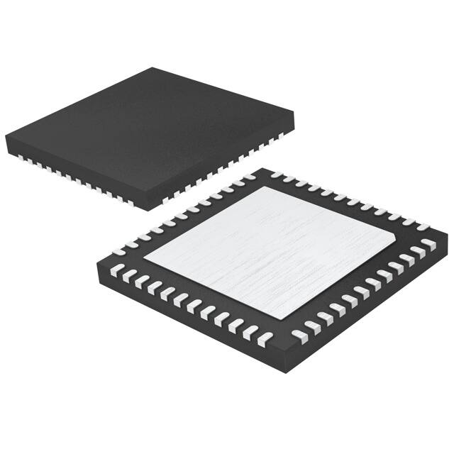
引脚分配: - 48个引脚分配在7mm x 7mm的QFN封装中,包括电源引脚、模拟输入引脚、时钟输入、数字输出等。

参数特性: - 采样率:LTC2203为25Msps,LTC2202为10Msps。 - 信噪比(SNR):最高可达81.6dB。 - 无杂散动态范围(SFDR):在特定条件下可达100dB。 - 输入范围:可通过PGA前端优化,支持2.5VP-P或1.667VP-P的输入范围。

功能详解: - 器件具有可选的内部抖动功能,以改善低信号水平下的SFDR。 - 提供单独的输出电源,允许CMOS输出摆幅在0.5V至3.6V范围内变化。 - 具有时钟占空比稳定器,可在全速下与宽范围的时钟占空比保持高性能。

应用信息: - 适用于电信、接收器、蜂窝基站、频谱分析、成像系统和自动测试设备(ATE)等领域。

封装信息: - 采用48引脚的塑料QFN封装,尺寸为7mm x 7mm,暴露的垫片是地线(GND)。
LTC2202IUK#PBF 价格&库存

很抱歉,暂时无法提供与“LTC2202IUK#PBF”相匹配的价格&库存,您可以联系我们找货

免费人工找货