物料型号:
- LTC2205/LTC2204
器件简介:
- LTC2205/LTC2204是16位模数转换器(ADC),专为数字化高频、宽动态范围信号设计,输入频率高达700MHz。这些ADC具有PGA前端,可以优化输入范围,非常适合要求严格的通信应用。
引脚分配:
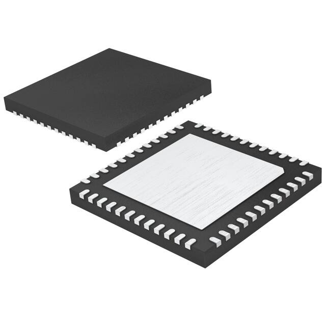
- 文档提供了详细的引脚分配图和说明,包括电源引脚、模拟输入引脚、数字输出引脚等。
参数特性:
- 采样率:LTC2205为65Msps,LTC2204为40Msps。
- 信噪比(SNR):79dB。
- 无杂散动态范围(SFDR):100dB。
- 输入范围可调节,最大直流规格包括±4LSB的积分非线性(INL)和±1LSB的微分非线性(DNL)。
功能详解:
- 包括对PGA前端、采样率、内部抖动、数据输出随机器、时钟占空比稳定器等功能的详细描述。
应用信息:
- 适用于电信接收器、蜂窝基站、频谱分析、成像系统和自动测试设备(ATE)。
封装信息:
- 48引脚(7mm × 7mm)塑料QFN封装。