LTC2273/LTC2272
16-Bit, 80Msps/65Msps
Serial Output ADC
DESCRIPTION
FEATURES
n
High Speed Serial Interface (JESD204)
Sample Rate: 80Msps/65Msps
77.7dBFS Noise Floor
100dB SFDR
SFDR >90dB at 140MHz (1.5VP-P Input Range)
PGA Front End (2.25VP-P or 1.5VP-P Input Range)
700MHz Full Power Bandwidth S/H
Optional Internal Dither
Single 3.3V Supply
Power Dissipation: 1100mW/990mW
Clock Duty Cycle Stabilizer
Pin Compatible Family
105Msps: LTC2274
80Msps: LTC2273
65Msps: LTC2272
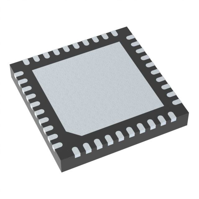
40-Pin 6mm × 6mm QFN Package
n
n
n
n
n
n
n
n
n
n
n
n
The LTC®2273/LTC2272 are 80Msps/65Msps, 16-bit A/D
converters with a high speed serial interface. They are
designed for digitizing high frequency, wide dynamic
range signals with an input bandwidth of 700MHz. The
input range of the ADC can be optimized using the PGA
front end. The output data is serialized according to the
JEDEC serial interface for data converters specification
(JESD204).
The LTC2273/LTC2272 are perfect for demanding applications where it is desirable to isolate the sensitive analog
circuits from the noisy digital logic. The AC performance
includes a 77.7dB Noise Floor and 100dB spurious free
dynamic range (SFDR). Ultra low internal jitter of 80fs
RMS allows undersampling of high input frequencies
with excellent noise performance. Maximum DC specs
include ±4.5LSB INL and ±1LSB DNL (no missing codes)
over temperature.
APPLICATIONS
n
The encode clock inputs, ENC+ and ENC–, may be driven
differentially or single-ended with a sine wave, PECL,
LVDS, TTL or CMOS inputs. A clock duty cycle stabilizer
allows high performance at full speed with a wide range
of clock duty cycles.
Telecommunications
Receivers
Cellular Base Stations
Spectrum Analysis
Imaging Systems
ATE
n
n
n
n
n
L, LT, LTC, LTM, Linear Technology and the Linear logo are registered trademarks of Linear
Technology Corporation. All other trademarks are the property of their respective owners.
TYPICAL APPLICATION
3.3V
SENSE
VCM
1.25V
COMMON MODE
BIAS VOLTAGE
FAM
128k Point FFT, fIN = 4.93MHz,
–1dBFS, PGA = 0
SYNC+
INTERNAL ADC
REFERENCE
GENERATOR
SYNC–
8B/10B
ENCODER
OVDD
ASIC OR FPGA
1.2V TO 3.3V
2.2μF
16
50Ω
0.1μF
20
AIN +
CMLOUT+
+
ANALOG
INPUT
AIN –
16-BIT
PIPELINED
ADC CORE
S/H
AMP
–
AMPLITUDE (dBFS)
50Ω
+
SERIAL
RECEIVER
SERIALIZER
CORRECTION
LOGIC
–
CMLOUT–
CLOCK
SCRAMBLER/
PATTERN
GENERATOR
CLOCK/DUTY
CYCLE
CONTROL
ENC+
ENC–
VDD
20X
PLL
GND
3.3V
0.1μF
0.1μF
22732 TA01
PGA DITH MSBINV SHDN
0
–10
–20
–30
–40
–50
–60
–70
–80
–90
–100
–110
–120
–130
0
10
20
30
FREQUENCY (MHz)
40
22732 G04
PAT1 PAT0 SCRAM SRR1 SRR0
22732fa
1
�LTC2273/LTC2272
ABSOLUTE MAXIMUM RATINGS
PIN CONFIGURATION
OVDD = VDD (Notes 1, 2)
FAM
PAT0
PAT1
SCRAM
PGA
MSBINV
GND
SENSE
GND
Supply Voltage (VDD) ................................... –0.3V to 4V
Analog Input Voltage (Note 3) .......–0.3V to (VDD + 0.3V)
Digital Input Voltage......................–0.3V to (VDD + 0.3V)
Digital Output Voltage ................ –0.3V to (OVDD + 0.3V)
Power Dissipation .............................................2000mW
Operating Temperature Range
LTC2273C/LTC2272C ............................... 0°C to 70°C
LTC2273I/LTC2272I.............................. –40°C to 85°C
Storage Temperature Range................... –65°C to 150°C
Digital Output Supply Voltage (OVDD) .......... –0.3V to 4V
VCM
TOP VIEW
40 39 38 37 36 35 34 33 32 31
VDD 1
30 GND
VDD 2
29 SYNC–
GND 3
28 SYNC+
AIN+ 4
27 GND
AIN– 5
26 GND
41
GND 6
25 OVDD
GND 7
24 CMLOUT+
GND 8
23 CMLOUT–
ENC+ 9
22 OVDD
ENC– 10
21 GND
SHDN
SHDN
SRR1
SRR0
ISMODE
DITH
GND
VDD
VDD
GND
11 12 13 14 15 16 17 18 19 20
UJ PACKAGE
40-LEAD (6mm s 6mm) PLASTIC QFN
TJMAX = 150°C, θJA = 22°C/W
EXPOSED PAD (PIN 41) IS GND, MUST BE SOLDERED TO PCB
ORDER INFORMATION
LEAD FREE FINISH
TAPE AND REEL
PART MARKING*
PACKAGE DESCRIPTION
TEMPERATURE RANGE
LTC2273CUJ#PBF
LTC2273CUJ#TRPBF
LTC2273UJ
40-Lead (6mm × 6mm) Plastic QFN
0°C to 70°C
LTC2273IUJ#PBF
LTC2273IUJ#TRPBF
LTC2273UJ
40-Lead (6mm × 6mm) Plastic QFN
–40°C to 85°C
LTC2272CUJ#PBF
LTC2272CUJ#TRPBF
LTC2272UJ
40-Lead (6mm × 6mm) Plastic QFN
0°C to 70°C
LTC2272IUJ#PBF
LTC2272IUJ#TRPBF
LTC2272UJ
40-Lead (6mm × 6mm) Plastic QFN
–40°C to 85°C
LEAD BASED FINISH
TAPE AND REEL
PART MARKING*
PACKAGE DESCRIPTION
TEMPERATURE RANGE
LTC2273CUJ
LTC2273CUJ#TR
LTC2273UJ
40-Lead (6mm × 6mm) Plastic QFN
0°C to 70°C
LTC2273IUJ
LTC2273IUJ#TR
LTC2273UJ
40-Lead (6mm × 6mm) Plastic QFN
–40°C to 85°C
LTC2272CUJ
LTC2272CUJ#TR
LTC2272UJ
40-Lead (6mm × 6mm) Plastic QFN
0°C to 70°C
LTC2272IUJ
LTC2272IUJ#TR
LTC2272UJ
40-Lead (6mm × 6mm) Plastic QFN
–40°C to 85°C
Consult LTC Marketing for parts specified with wider operating temperature ranges. *The temperature grade is identified by a label on the shipping container.
For more information on lead free part marking, go to: http://www.linear.com/leadfree/
For more information on tape and reel specifications, go to: http://www.linear.com/tapeandreel/
CONVERTER CHARACTERISTICS The l denotes the specifications which apply over the full operating
temperature range, otherwise specifications are at TA = 25°C. (Note 4)
SYMBOL
Integral Linearity Error
Integral Linearity Error
Differential Linearity Error
Offset Error
Offset Drift
Gain Error
Full-Scale Drift
Transition Noise
CONDITIONS
Differential Analog Input (Note 5) TA = 25°C
Differential Analog Input (Note 5)
Differential Analog Input
(Note 6)
External Reference
Internal Reference
External Reference
MIN
l
l
l
l
TYP
±1.2
±1.5
±0.3
±1
±10
±0.2
±30
±15
3
MAX
±4
±4.5
±1
±8.5
±1.5
UNITS
LSB
LSB
LSB
mV
μV/°C
%FS
ppm/°C
ppm/°C
LSBRMS
22732fa
2
�LTC2273/LTC2272
ANALOG INPUT
The l denotes denotes the specifications which apply over the full operating temperature range,
otherwise specifications are at TA = 25°C. (Note 4)
SYMBOL
PARAMETER
CONDITIONS
VIN
Analog Input Range (AIN+ – AIN–)
3.135V ≤ VDD ≤ 3.465V
l
MIN
VIN, CM
Analog Input Common Mode
Differential Input (Note 7)
l
1
IIN
Analog Input Leakage Current
0V ≤ AIN+, AIN– ≤ VDD (Note 10)
l
ISENSE
SENSE Input Leakage Current
0V ≤ SENSE ≤ VDD (Note 11)
CIN
Analog Input Capacitance
Sample Mode ENC+ < ENC–
Hold Mode ENC+ > ENC–
tAP
TYP
MAX
UNITS
1.5 or 2.25
1.25
VP-P
1.5
V
–1
1
μA
–3
3
μA
6.7
1.8
pF
pF
Sample-and-Hold
Acquisition Delay Time
1
ns
tJITTER
Sample-and-Hold
Acquisition Delay Time Jitter
80
fsRMS
CMRR
Analog Input
Common Mode Rejection Ratio
1V < (AIN+ = AIN–)
很抱歉,暂时无法提供与“LTC2273CUJ”相匹配的价格&库存,您可以联系我们找货
免费人工找货