Order
Now
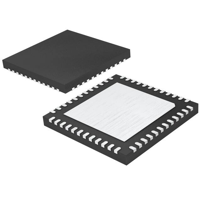
Product
Folder
Technical
Documents
Support &
Community
Tools &
Software
ADS8588H
SBAS843 – SEPTEMBER 2017
ADS8588H 16-Bit, 500-kSPS, 8-Channel, Simultaneous-Sampling ADC With
Bipolar Inputs on a Single Supply
1 Features
3 Description
•
•
•
•
•
•
•
•
The ADS8588H device is an 8-channel, integrated
data acquisition (DAQ) system based on a 16-bit
successive approximation (SAR) analog-to-digital
converter
(ADC).
All
input
channels
are
simultaneously sampled to achieve a maximum
throughput of 500 kSPS per channel. The device
features a complete analog front-end for each
channel, including a programmable gain amplifier
(PGA) with a high input impedance of 1 MΩ, an input
clamp, low-pass filter, and an ADC input driver. The
device also features a low-drift, precision reference
with a buffer to drive the ADC. A flexible digital
interface supporting serial, parallel, and parallel byte
communication enables the device to be used with a
variety of host controllers.
1
•
•
•
•
•
16-Bit ADC With Integrated Analog Front-End
Simultaneous Sampling: 8 Channels
Pin-Programmable Bipolar Inputs: ±10 V and ±5 V
High Input Impedance: 1 MΩ
5-V Analog Supply: 2.3-V to 5-V I/O Supply
Overvoltage Input Clamp With 9-kV ESD
Low-Drift, On-Chip Reference (2.5 V) and Buffer
Performance:
– 500-kSPS Max Throughput on All Channels
– DNL: ±0.3 LSB Typ; INL: ±0.5 LSB Typ
– SNR: 92.7 dB Typ; THD: −110 dB Typ
Over Temperature Performance:
– Max Offset Drift: 3 ppm/°C
– Gain Drift: 6 ppm/°C
On-Chip Digital Filter for Oversampling
Flexible Parallel, Byte, and Serial Interface
Temperature Range: –40°C to +125°C
Package: LQFP-64
The ADS8588H can be configured to accept ±10-V or
±5-V true bipolar inputs using a single 5-V supply.
The high input impedance allows direct connection
with sensors and transformers, thus eliminating the
need for external driver circuits. The high
performance and accuracy, along with zero-latency
conversions offered by this device, also means the
ADS8588H meets the strict design requirements for
many industrial automation and control applications.
2 Applications
•
•
•
•
•
Device Information(1)
Monitoring and Control for Power Grids
Protection Relays
Multi-Phase Motor Controls
Industrial Automation and Controls
Multichannel Data Acquisition Systems
PART NUMBER
PACKAGE
ADS8588H
LQFP (64)
BODY SIZE (NOM)
10.00 mm × 10.00 mm
(1) For all available packages, see the orderable addendum at
the end of the datasheet.
Device Block Diagram
DVDD
AVDD
BUSY
ADS8588H
FRSTDATA
STBY
1 M:
AIN_1P
AIN_1GND
Clamp
PGA
Clamp
3rd-Order
LPF
ADC
Driver
CONVSTA, CONVSTB
16-Bit
SAR
ADC
RESET
RANGE
1 M:
CS
RD/SCLK
1 M:
AIN_2P
AIN_2GND
Clamp
PGA
Clamp
3rd-Order
LPF
ADC
Driver
16-Bit
SAR
ADC
1 M:
SAR
Logic
and
Digital Control
PAR/SER
SER/PAR Interface
DB[15:0]
DOUTA
DOUTB
OS0
Digital Filter
Clamp
PGA
AIN_7GND
OS1
OS2
1 M:
AIN_7P
Clamp
3rd-Order
LPF
ADC
Driver
16-Bit
SAR
ADC
ADC
Driver
16-Bit
SAR
ADC
REFCAPA
1 M:
REFCAPB
1 M:
AIN_8P
AIN_8GND
Clamp
PGA
Clamp
3rd-Order
LPF
2.5 VREF
REFIN/REFOUT
1 M:
REFSEL
AGND
REFGND
Copyright © 2017, Texas Instruments Incorporated
1
An IMPORTANT NOTICE at the end of this data sheet addresses availability, warranty, changes, use in safety-critical applications,
intellectual property matters and other important disclaimers. PRODUCTION DATA.
�ADS8588H
SBAS843 – SEPTEMBER 2017
www.ti.com
Table of Contents
1
2
3
4
5
6
Features ..................................................................
Applications ...........................................................
Description .............................................................
Revision History.....................................................
Pin Configuration and Functions .........................
Specifications.........................................................
Operation, CS and RD Separate .............................
6.18 Switching Characteristics: Serial Data Read
Operation .................................................................
6.19 Switching Characteristics: Byte Mode Data Read
Operation .................................................................
6.20 Typical Characteristics ..........................................
1
1
1
2
3
5
7
6.1
6.2
6.3
6.4
6.5
6.6
6.7
6.8
Absolute Maximum Ratings ...................................... 5
ESD Ratings.............................................................. 5
Recommended Operating Conditions....................... 6
Thermal Information .................................................. 6
Electrical Characteristics........................................... 7
Timing Requirements: CONVST Control ................ 10
Timing Requirements: Data Read Operation.......... 10
Timing Requirements: Parallel Data Read Operation,
CS and RD Tied Together ....................................... 10
6.9 Timing Requirements: Parallel Data Read Operation,
CS and RD Separate ............................................... 11
6.10 Timing Requirements: Serial Data Read
Operation ................................................................. 11
6.11 Timing Requirements: Byte Mode Data Read
Operation ................................................................. 11
6.12 Timing Requirements: Oversampling Mode.......... 11
6.13 Timing Requirements: Exit Standby Mode............ 11
6.14 Timing Requirements: Exit Shutdown Mode......... 12
6.15 Switching Characteristics: CONVST Control ........ 12
6.16 Switching Characteristics: Parallel Data Read
Operation, CS and RD Tied Together ..................... 12
6.17 Switching Characteristics: Parallel Data Read
13
13
17
Detailed Description ............................................ 24
7.1
7.2
7.3
7.4
8
13
Overview .................................................................
Functional Block Diagram .......................................
Feature Description.................................................
Device Functional Modes........................................
24
24
25
34
Application and Implementation ........................ 47
8.1 Application Information............................................ 47
8.2 Typical Application ................................................. 47
9 Power Supply Recommendations...................... 51
10 Layout................................................................... 52
10.1 Layout Guidelines ................................................. 52
10.2 Layout Example .................................................... 52
11 Device and Documentation Support ................. 54
11.1
11.2
11.3
11.4
11.5
11.6
Documentation Support ........................................
Receiving Notification of Documentation Updates
Community Resources..........................................
Trademarks ...........................................................
Electrostatic Discharge Caution ............................
Glossary ................................................................
54
54
54
54
54
54
12 Mechanical, Packaging, and Orderable
Information ........................................................... 54
4 Revision History
NOTE: Page numbers for previous revisions may differ from page numbers in the current version.
2
DATE
REVISION
NOTES
September 2017
*
Initial release.
Submit Documentation Feedback
Copyright © 2017, Texas Instruments Incorporated
Product Folder Links: ADS8588H
�ADS8588H
www.ti.com
SBAS843 – SEPTEMBER 2017
5 Pin Configuration and Functions
AIN_8GND
AIN_8P
AIN_7GND
AIN_7P
AIN_6GND
AIN_6P
AIN_5GND
AIN_5P
AIN_4GND
AIN_4P
AIN_3GND
AIN_3P
AIN_2GND
AIN_2P
AIN_1GND
AIN_1P
64
63
62
61
60
59
58
57
56
55
54
53
52
51
50
49
PM Package
64-Pin LQFP
Top View
OS2
5
44
REFCAPA
PAR/SER/BYTE_SEL
6
43
REFGND
STBY
7
42
REFIN/REFOUT
RANGE
8
41
AGND
CONVSTA
9
40
AGND
CONVSTB
10
39
REGCAP2
RESET
11
38
AVDD
RD/SCLK
12
37
AVDD
CS
13
36
REGCAP1
BUSY
14
35
AGND
FRSTDATA
15
34
REFSEL
DB0
16
33
DB15/BYTE_SEL
DB14/HBEN
DB13
DB12
DB11
DB10
DB9
AGND
DB8/DOUTB
DB7/DOUTA
DVDD
DB6
DB5
DB4
DB3
DB2
DB1
32
REFCAPB
31
45
30
4
29
OS1
28
REFGND
27
46
26
3
25
OS0
24
AGND
23
47
22
2
21
AGND
20
AVDD
19
48
18
1
17
AVDD
Not to scale
Pin Functions
PIN
NAME
NO.
TYPE
DESCRIPTION
2, 26, 35, 40,
41, 47
P
Analog ground pins
AIN_1GND
50
AI
Analog input channel 1: negative input.
AIN_1P
49
AI
Analog input channel 1: positive input.
AIN_2GND
52
AI
Analog input channel 2: negative input.
AIN_2P
51
AI
Analog input channel 2: positive input.
AIN_3GND
54
AI
Analog input channel 3: negative input.
AGND
Submit Documentation Feedback
Copyright © 2017, Texas Instruments Incorporated
Product Folder Links: ADS8588H
3
�ADS8588H
SBAS843 – SEPTEMBER 2017
www.ti.com
Pin Functions (continued)
PIN
NAME
NO.
TYPE
DESCRIPTION
AIN_3P
53
AI
Analog input channel 3: positive input.
AIN_4GND
56
AI
Analog input channel 4: negative input.
AIN_4P
55
AI
Analog input channel 4: positive input.
AIN_5GND
58
AI
Analog input channel 5: negative input.
AIN_5P
57
AI
Analog input channel 5: positive input.
AIN_6GND
60
AI
Analog input channel 6: negative input.
AIN_6P
59
AI
Analog input channel 6: positive input.
AIN_7GND
62
AI
Analog input channel 7: negative input.
AIN_7P
61
AI
Analog input channel 7: positive input.
AIN_8GND
64
AI
Analog input channel 8: negative input.
AIN_8P
63
AI
Analog input channel 8: positive input.
AVDD
1, 37, 38, 48
P
Analog supply pins. Decouple these pins to the closest AGND pins
(see the Power Supply Recommendations section).
BUSY
14
DO
Active high digital output indicating ongoing conversion
(see the BUSY (Output) section).
CONVSTA
9
DI
Active high logic input to control start of conversion for first half count of device input channels (see the
CONVSTA, CONVSTB (Input) section).
CONVSTB
10
DI
Active high logic input to control start of conversion for second half count of device input channels (see
the CONVSTA, CONVSTB (Input) section).
CS
13
DI
Active low logic input chip-select signal (see the CS (Input) section).
DB0
16
DO
Data output DB0 (LSB) in parallel interface mode (see the DB[6:0] section).
DB1
17
DO
Data output DB1 in parallel interface mode (see the DB[6:0] section).
DB2
18
DO
Data output DB2 in parallel interface mode (see the DB[6:0] section).
DB3
19
DO
Data output DB3 in parallel interface mode (see the DB[6:0] section).
DB4
20
DO
Data output DB4 in parallel interface mode (see the DB[6:0] section).
DB5
21
DO
Data output DB5 in parallel interface mode (see the DB[6:0] section).
DB6
22
DO
Data output DB6 in parallel interface mode (see the DB[6:0] section).
DB7/DOUTA
24
DO
Multi-function logic output pin (see the DB7/DOUTA section):
this pin is data output DB7 in parallel and parallel byte interface mode;
this pin is a data output pin in serial interface mode.
DB8/DOUTB
25
DO
Multi-function logic output pin (see the DB8/DOUTB section):
this pin is data output DB8 in parallel interface mode;
this pin is a data output pin in serial interface mode.
DB9
27
DO
Data output DB9 in parallel interface mode (see the DB[13:9] section).
DB10
28
DO
Data output DB10 in parallel interface mode (see the DB[13:9] section).
DB11
29
DO
Data output DB11 in parallel interface mode (see the DB[13:9] section).
DB12
30
DO
Data output DB12 in parallel interface mode (see the DB[13:9] section).
DB13
31
DO
Data output DB13 in parallel interface mode (see the DB[13:9] section).
DB14
32
DO
Multi-function logic input or output pin (see the DB14/HBEN section):
this pin is data output DB14 in parallel interface mode;
this pin is a control input pin for byte selection (high or low) in parallel byte interface mode.
DB15
33
DO
Multi-function logic input or output pin (see the DB14/HBEN section):
this pin is data output DB14 in parallel interface mode;
this pin is a control input pin for byte selection (high or low) in parallel byte interface mode.
DVDD
23
P
FRSTDATA
15
DO
Active high digital output indicating data read back from channel 1 of the devices (see the FRSTDATA
(Output) section).
OS0
3
DI
Oversampling mode control pin
(see the Oversampling Mode of Operation section).
OS1
4
DI
Oversampling mode control pin
(see the Oversampling Mode of Operation section).
OS2
5
DI
Oversampling mode control pin
(see the Oversampling Mode of Operation section).
PAR/SER/BYTE SEL
6
DI
Logic input pin to select between parallel or serial or parallel byte interface mode (see the Data Read
Operation section).
4
Digital supply pin; decouple with AGND on pin 26.
Submit Documentation Feedback
Copyright © 2017, Texas Instruments Incorporated
Product Folder Links: ADS8588H
�ADS8588H
www.ti.com
SBAS843 – SEPTEMBER 2017
Pin Functions (continued)
PIN
NAME
NO.
TYPE
DESCRIPTION
RANGE
8
DI
Multi-function logic input pin (see the RANGE (Input) section):
when the STBY pin is high, this pin selects the input range of the device (+/-10 V or +/-5 V); when the
STBY pin is low, this pin selects between the standby and shutdown modes.
RD/SCLK
12
DI
Multi-function logic input pin (see the RD/SCLK (Input) section):
this pin is an active-low ready input pin in parallel and parallel byte interface;
this pin is a clock input pin in serial interface mode.
REFCAPA
44
AO
Reference amplifier output pins. This pin must be shorted to REFCAPB and decoupled to AGND using a
low ESR, 22-µF ceramic capacitor.
REFCAPB
45
AO
Reference amplifier output pins. This pin must be shorted to REFCAPA and decoupled to AGND using a
low ESR, 22-µF ceramic capacitor.
REFGND
43, 46
P
REFIN/REFOUT
42
AIO
REFSEL
34
DI
Active high logic input to enable the internal reference
(see the REFSEL (Input) section).
REGCAP1
36
AO
Output pin 1 for the internal voltage regulator; decouple separately to AGND using a 1-µF capacitor.
REGCAP2
39
AO
Output pin 2 for the internal voltage regulator; decouple separately to AGND using a 1-µF capacitor.
RESET
11
DI
Active high logic input to reset the device digital logic
(see the REFSEL (Input) section).
STBY
7
DI
Active low logic input to enter the device into one of the two power-down modes: standby or shutdown
(see the Power-Down Modes section).
Reference GND pin. This pin must be shorted to the analog GND plane and decoupled with
REFIN/REFOUT on pin 42 using a 10-µF capacitor.
This pin acts as an internal reference output when REFSEL is high;
this pin functions as an input pin for the external reference when REFSEL is low;
decouple with REFGND on pin 43 using a 10-µF capacitor.
6 Specifications
6.1 Absolute Maximum Ratings
at TA = 25°C (unless otherwise noted) (1)
MIN
MAX
UNIT
AVDD to AGND
–0.3
7.0
V
DVDD to AGND
–0.3
7.0
V
Analog input voltage to AGND (2)
–15
15
V
Digital input to AGND
–0.3
DVDD + 0.3
V
REFIN to AGND
–0.3
AVDD + 0.3
V
Input current to any pin except supplies (2)
–10
10
mA
–40
125
Operating
Temperature
Junction, TJ
150
Storage, Tstg
(1)
(2)
–65
°C
150
Stresses beyond those listed under Absolute Maximum Ratings may cause permanent damage to the device. These are stress ratings
only, which do not imply functional operation of the device at these or any other conditions beyond those indicated under Recommended
Operating Conditions. Exposure to absolute-maximum-rated conditions for extended periods may affect device reliability.
Transient currents of up to 100 mA do not cause SCR latch-up.
6.2 ESD Ratings
VALUE
V(ESD)
Electrostatic discharge
Human-body model (HBM), per
ANSI/ESDA/JEDEC JS-001 (1)
All pins except analog inputs
±2000
Analog input pins only
±9000
Charged-device model (CDM), per JEDEC specification JESD22-C101
(1)
(2)
(2)
UNIT
V
±500
JEDEC document JEP155 states that 500-V HBM allows safe manufacturing with a standard ESD control process.
JEDEC document JEP157 states that 250-V CDM allows safe manufacturing with a standard ESD control process.
Submit Documentation Feedback
Copyright © 2017, Texas Instruments Incorporated
Product Folder Links: ADS8588H
5
�ADS8588H
SBAS843 – SEPTEMBER 2017
www.ti.com
6.3 Recommended Operating Conditions
over operating free-air temperature range (unless otherwise noted)
MIN
NOM
MAX
UNIT
AVDD
Analog supply voltage
4.75
5
5.25
V
DVDD
Digital supply voltage
2.3
3.3
AVDD
V
6.4 Thermal Information
ADS8588H
THERMAL METRIC (1)
PM (LQFP)
UNIT
64 PINS
RθJA
Junction-to-ambient thermal resistance
46.0
°C/W
RθJC(top)
Junction-to-case (top) thermal resistance
7.8
°C/W
RθJB
Junction-to-board thermal resistance
20.1
°C/W
ψJT
Junction-to-top characterization parameter
0.3
°C/W
ψJB
Junction-to-board characterization parameter
19.6
°C/W
RθJC(bot)
Junction-to-case (bottom) thermal resistance
N/A
°C/W
(1)
6
For more information about traditional and new thermal metrics, see the Semiconductor and IC Package Thermal Metrics application
report.
Submit Documentation Feedback
Copyright © 2017, Texas Instruments Incorporated
Product Folder Links: ADS8588H
�ADS8588H
www.ti.com
SBAS843 – SEPTEMBER 2017
6.5 Electrical Characteristics
minimum and maximum specifications are at TA = –40°C to +125°C, AVDD = 4.75 V to 5.25 V; typical specifications are at TA
= 25°C; AVDD = 5 V, DVDD = 3 V, VREF = 2.5 V (internal), and fSAMPLE = 500 kSPS (unless otherwise noted)
PARAMETER
TEST CONDITIONS
MIN
TYP
MAX
UNIT
ANALOG INPUTS
Full-scale input span (1)
(AIN_nP to AIN_nGND)
RANGE pin = 1
–10
10
RANGE pin = 0
–5
5
AIN_nP
Operating input range,
positive input
RANGE pin = 1
–10
10
RANGE pin = 0
–5
5
AIN_nGND
Operating input range,
negative input
RANGE pin = 1
–0.3
0
0.3
RANGE pin = 0
–0.3
0
0.3
RIN
Input impedance
At TA = 25°C
0.85
1
1.15
Input impedance drift
All input ranges
–25
±7
25
Input leakage current
With voltage at AIN_nP = VIN,
all input ranges
IIkg(in)
(VIN – 2) / RIN
V
V
V
MΩ
ppm/°C
µA
SYSTEM PERFORMANCE
Resolution
16
NMC
No missing codes
16
DNL
Differential nonlinearity
All input ranges
–0.6
±0.3
0.6
LSB (2)
INL
Integral nonlinearity (3)
All input ranges
–1.5
±0.5
1.5
LSB
TA = –40°C to
+85°C
–64
±4
64
Gain error (4)
All input ranges,
external
reference
TA = –40°C to
+125°C
–64
±4
96
EG
Gain error matching
(channel-to-channel)
Gain error temperature drift
EO
Offset error
Bits
Bits
All input ranges,
internal reference
±4
Input range = ±10 V,
external and internal reference
10
60
Input range = ±5 V,
external and internal reference
12
60
±6
14
All input ranges,
external reference
LSB
LSB
–14
ppm/°C
All input ranges,
internal reference
±10
Input range = ±10 V
–3
±0.2
3
Input range = ±5 V
–3
±0.15
3
0.7
5
mV
±0.3
3
ppm/°C
Offset error matching
(channel-to-channel)
All input ranges
Offset error temperature drift
All input ranges
–3
mV
SAMPLING DYNAMICS
tACQ
Acquisition time
fS
Maximum throughput rate per channel
without latency
(1)
(2)
(3)
(4)
0.7
All eight channels included
µs
500
kSPS
Ideal input span, does not include gain or offset error.
LSB = least significant bit.
This parameter is the endpoint INL, not best-fit INL.
Gain error is calculated after adjusting for offset error, which implies that the positive full-scale error = negative full-scale error = gain
error ÷ 2.
Submit Documentation Feedback
Copyright © 2017, Texas Instruments Incorporated
Product Folder Links: ADS8588H
7
�ADS8588H
SBAS843 – SEPTEMBER 2017
www.ti.com
Electrical Characteristics (continued)
minimum and maximum specifications are at TA = –40°C to +125°C, AVDD = 4.75 V to 5.25 V; typical specifications are at TA
= 25°C; AVDD = 5 V, DVDD = 3 V, VREF = 2.5 V (internal), and fSAMPLE = 500 kSPS (unless otherwise noted)
PARAMETER
TEST CONDITIONS
MIN
TYP
MAX
UNIT
DYNAMIC CHARACTERISTICS
Signal-to-noise ratio,
no oversampling
(VIN – 0.5 dBFS at 1 kHz)
Input range = ±10 V
91
92.7
SNR
Input range = ±5 V
89.5
92.1
Signal-to-noise ratio,
oversampling = 32x
(VIN – 0.5 dBFS at 130 Hz)
Input range = ±10 V
95.5
96.9
SNROSR
94
95.8
THD
Total harmonic distortion (5)
(VIN – 0.5 dBFS at 1 kHz)
Signal-to-noise + distortion ratio,
no oversampling
(VIN – 0.5 dBFS at 1 kHz)
Input range = ±10 V
90.9
92.6
SINAD
Input range = ±5 V
89.2
92
Signal-to-noise + distortion ratio,
oversampling = 16 x
(VIN – 0.5 dBFS at 130 Hz)
Input range = ±10 V
94.75
96.5
SINADOSR
Input range = ±5 V
93.5
95.3
SFDR
Spurious-free dynamic range
(VIN – 0.5 dBFS at 1 kHz)
Input range = ±5 V
All input ranges
–110
All input ranges
Crosstalk isolation (6)
BW(–3
dB)
BW(–0.1 dB)
tGROUP
Small-signal bandwidth, –3 dB
Small-signal bandwidth, –0.1 dB
Group delay
dB
dB
–95
dB
dB
dB
110
dB
–95
dB
At TA = 25°C,
input range = ±10 V
24
At TA = 25°C,
input range = ±5 V
16
At TA = 25°C,
input range = ±10 V
14
At TA = 25°C,
input range = ±5 V
9.5
Input range = ±10 V
13
Input range = ±5 V
19
kHz
kHz
µs
INTERNAL REFERENCE OUTPUT (REFSEL = 1)
Voltage on the REFIN/REFOUT pin
(configured as output)
VREF (7)
C(REFIN_
REFOUT)
V(REFCAP)
At TA = 25°C
2.4975
2.5025
V
Internal reference temperature drift
7.5
ppm/°C
Decoupling capacitor on
REFIN/REFOUT (8)
10
µF
Reference voltage to the ADC
(on the REFCAPA, REFCAPB pin)
At TA = 25°C
3.996
Reference buffer output impedance
Reference buffer output temperature drift
C(REFCAP)
2.5
Decoupling capacitor on REFCAPA,
REFCAPB
Turn-on time
C(REFCAP) = 10 µF,
C(REFIN_REFOUT) = 10 µF
4.0
4.004
0.5
1
V
Ω
5
ppm/°C
10
µF
25
ms
EXTERNAL REFERENCE INPUT (REFSEL = 0)
VREFIO_EXT
(5)
(6)
(7)
(8)
8
External reference voltage on REFIO
(configured as input)
2.475
2.5
2.525
V
Reference input impedance
100
MΩ
Reference input capacitance
10
pF
Calculated on the first nine harmonics of the input frequency.
Isolation crosstalk is measured by applying a full-scale sinusoidal signal up to 160 kHz to a channel, not selected in the multiplexing
sequence, and measuring the effect on the output of any selected channel.
Does not include the variation in voltage resulting from solder shift effects.
Recommended to use an X7R-grade, 0603-size ceramic capacitor for optimum performance (see the Layout Guidelines section).
Submit Documentation Feedback
Copyright © 2017, Texas Instruments Incorporated
Product Folder Links: ADS8588H
�ADS8588H
www.ti.com
SBAS843 – SEPTEMBER 2017
Electrical Characteristics (continued)
minimum and maximum specifications are at TA = –40°C to +125°C, AVDD = 4.75 V to 5.25 V; typical specifications are at TA
= 25°C; AVDD = 5 V, DVDD = 3 V, VREF = 2.5 V (internal), and fSAMPLE = 500 kSPS (unless otherwise noted)
PARAMETER
TEST CONDITIONS
MIN
TYP
MAX
UNIT
POWER-SUPPLY REQUIREMENTS
AVDD
Analog power-supply voltage
Analog supply
DVDD
Digital power-supply voltage
Digital supply range
IAVDD_DYN
IAVDD_STC
IAVDD_STDBY
Analog supply current
(operational)
Analog supply current
(static)
AVDD supply
STANDBY current
4.75
5
5.25
V
2.3
3.3
AVDD
V
AVDD = 5 V,
fS = 500 kSPS,
internal reference
22.8
30.8
AVDD = 5 V,
fS = 500 kSPS,
external reference
22.2
30
AVDD = 5 V, internal reference,
device not converting
12.7
17.4
AVDD = 5 V, external reference,
device not converting
12.3
16.7
At AVDD = 5 V, device in STDBY
mode,
internal reference
4.2
5.5
At AVDD = 5 V, device in STDBY
mode,
external reference
3.8
5
mA
mA
mA
IAVDD_PWR_ DN
AVDD supply
power-down current
At AVDD = 5 V, device in PWR_DN,
internal or
external reference,
TA = –40°C to +85°C
0.2
6
µA
IDVDD_DYN
Digital supply current
DVDD = 3.3 V, fS = 500 kSPS
0.2
0.33
mA
IDVDD_STDBY
DVDD supply STANDBY current
At AVDD = 5 V, device in STDBY
mode
0.05
1.5
µA
IDVDD_PWR-DN
DVDD supply power-down current
At AVDD = 5 V, device in PWR_DN
mode
0.05
1.5
µA
V
DIGITAL INPUTS (CMOS)
VIH
Digital high input voltage logic level
DVDD > 2.3 V
0.8 × DVDD
DVDD + 0.3
VIL
Digital low input voltage logic level
DVDD > 2.3 V
–0.3
0.2 × DVDD
V
Input leakage current
100
nA
Input pin capacitance
5
pF
DIGITAL OUTPUTS (CMOS)
VOH
Digital high output voltage logic level
IO = 100-µA source
VOL
Digital low output voltage logic level
IO = 100-µA sink
Floating state leakage current
Only for SDO
0.8 × DVDD
DVDD
0
0.2 × DVDD
Internal pin capacitance
V
V
1
µA
5
pF
TEMPERATURE RANGE
TA
Operating free-air temperature
–40
125
Submit Documentation Feedback
Copyright © 2017, Texas Instruments Incorporated
Product Folder Links: ADS8588H
°C
9
�ADS8588H
SBAS843 – SEPTEMBER 2017
www.ti.com
6.6 Timing Requirements: CONVST Control
minimum and maximum specifications are at TA = –40°C to +125°C, typical specifications are at TA = 25°C; AVDD = 5 V,
2.3 V ≤ DVDD ≤ 5.25 V, VREF = 2.5 V (internal), BUSY load = 20 pF, VIL and VIH at specified limits, and fSAMPLE = 500 kSPS
(unless otherwise noted) (see Figure 1)
MIN
NOM
MAX
UNIT
tACQ
Acquisition time:
BUSY falling edge to rising edge of trailing CONVSTA or CONVSTB
0.7
µs
tPH_CN
CONVSTA, CONVSTB pulse high time
25
ns
tPL_CN
CONVSTA, CONVSTB pulse low time
25
ns
tSU_BSYCS
Setup time: BUSY falling to CS falling
0
ns
tSU_RSTCN
Setup time: RESET falling to first rising edge of CONVSTA or CONVSTB
25
ns
tPH_RST
RESET pulse high time
50
tD_CNAB
Delay between rising edges of CONVSTA and CONVSTB
ns
500
µs
6.7 Timing Requirements: Data Read Operation
minimum and maximum specifications are at TA = –40°C to +125°C, typical specifications are at TA = 25°C; AVDD = 5 V,
2.3 V ≤ DVDD ≤ 5.25 V, VREF = 2.5 V (internal), BUSY load = 20 pF, VIL and VIH at specified limits, and fSAMPLE = 500 kSPS
(unless otherwise noted) (see Figure 2)
MIN
NOM
MAX
UNIT
tDZ_CNCS
Delay between CONVSTA, CONVSTB rising edge to CS falling edge, start of
data read operation during conversion
10
ns
tDZ_CSBSY
Delay between CS rising edge to BUSY falling edge, end of data read
operation during conversion
40
ns
tSU_BSYCS
Setup time: BUSY falling edge to CS falling edge, start of data read operation
after conversion
0
ns
tD_CSCN
Delay between CS rising edge to CONVSTA, CONVSTB rising edge, end of
data read operation after conversion
10
ns
6.8 Timing Requirements: Parallel Data Read Operation, CS and RD Tied Together
minimum and maximum specifications are at TA = –40°C to +125°C, typical specifications are at TA = 25°C; AVDD = 5 V,
2.3 V ≤ DVDD ≤ 5.25 V, VREF = 2.5 V (internal), load on DB[15:0] and FRSTDATA = 20 pF, VIL and VIH at specified limits, and
fSAMPLE = 500 kSPS (unless otherwise noted) (see Figure 3)
MIN
NOM
MAX
UNIT
tPH_CS,
tPH_RD
CS and RD high time
15
ns
tPL_CS,
tPL_RD
CS and RD low time
15
ns
2.5
ns
tHT_RDDB,
Hold time: RD and CS rising edge to DB[15:0] invalid
tHT_CSDB
10
Submit Documentation Feedback
Copyright © 2017, Texas Instruments Incorporated
Product Folder Links: ADS8588H
�ADS8588H
www.ti.com
SBAS843 – SEPTEMBER 2017
6.9 Timing Requirements: Parallel Data Read Operation, CS and RD Separate
minimum and maximum specifications are at TA = –40°C to +125°C, typical specifications are at TA = 25°C; AVDD = 5 V,
2.3 V ≤ DVDD ≤ 5.25 V, VREF = 2.5 V (internal), load on DB[15:0] and FRSTDATA = 20 pF, VIL and VIH at specified limits, and
fSAMPLE = 500 kSPS (unless otherwise noted) (see Figure 4)
MIN
NOM
MAX
UNIT
tSU_CSRD
Set-up time: CS falling edge to RD falling edge
0
ns
tHT_RDCS
Hold time: RD rising edge to CS rising edge
0
ns
tPL_RD
RD low time
15
ns
tPH_RD
RD high time
15
ns
tHT_CSDB
Hold time: CS rising edge to DB[15:0] becoming invalid
6
ns
tHT_RDDB
Hold time: RD rising edge to DB[15:0] becoming invalid
2.5
ns
6.10 Timing Requirements: Serial Data Read Operation
minimum and maximum specifications are at TA = –40°C to +125°C, typical specifications are at TA = 25°C; AVDD = 5 V,
2.3 V ≤ DVDD ≤ 5.25 V, VREF = 2.5 V (internal), load on DOUTA, DOUTB, and FRSTDATA = 20 pF, VIL and VIH at specified
limits, and fSAMPLE = 500 kSPS (unless otherwise noted) (see Figure 5)
MIN
NOM
MAX
UNIT
0.45
0.55
tSCLK
0.45
0.55
tSCLK
tSCLK
SCLK time period
50
tPH_SCLK
SCLK high time
ns
tPL_SCLK
SCLK low time
tHT_CKDO
Hold time: SCLK rising edge to DOUTA, DOUTB invalid
7
ns
tSU_CSCK
Setup time: CS falling to first SCLK edge
8
ns
tHT_CKCS
Hold time: last SCLK active edge to CS high
10
ns
6.11 Timing Requirements: Byte Mode Data Read Operation
minimum and maximum specifications are at TA = –40°C to +125°C, typical specifications are at TA = 25°C; AVDD = 5 V,
2.3 V ≤ DVDD ≤ 5.25 V, VREF = 2.5 V (internal), load on DB[7:0] and FRSTDATA = 20 pF, VIL and VIH at specified limits, and
fSAMPLE = 500 kSPS (unless otherwise noted) (see Figure 6)
MIN
NOM
MAX
UNIT
tSU_CSRD
Setup time: CS falling edge to RD falling edge
0
ns
tHT_RDCS
Hold time: RD rising edge to CS rising edge
0
ns
tPL_RD
RD low time
15
ns
tPH_RD
RD high time
15
ns
tHT_CSDB
Hold time: CS rising edge to DB[15:0] becoming invalid
6
ns
tHT_RDDB
Hold time: RD rising edge to DB[15:0] becoming invalid
2.5
ns
6.12 Timing Requirements: Oversampling Mode
minimum and maximum specifications are at TA = –40°C to +125°C, typical specifications are at TA = 25°C; AVDD = 5 V,
2.3 V ≤ DVDD ≤ 5.25 V, VREF = 2.5 V (internal), load on DB[7:0] and FRSTDATA = 20 pF, VIL and VIH at specified limits, and
fSAMPLE = 500 kSPS (unless otherwise noted) (see Figure 6)
MIN
NOM
MAX
UNIT
tHT_OS
Hold time: BUSY falling to OSx
20
ns
tSU_OS
Setup time: BUSY falling to OSx
20
ns
6.13 Timing Requirements: Exit Standby Mode
minimum and maximum specifications are at TA = –40°C to +125°C, typical specifications are at TA = 25°C, AVDD = 5 V,
2.3 V ≤ DVDD ≤ 5.25 V, VREF = 2.5 V (internal), VIL and VIH at specified limits, and fSAMPLE = 500 kSPS (unless otherwise
noted) (see Figure 8)
MIN
tD_STBYCN
(1)
Delay between STBY rising edge to CONVSTA or CONVSTB rising edge (1)
NOM
MAX
UNIT
100
µs
First conversion data must be discarded or RESET must be issued if the maximum timing is exceeded.
Submit Documentation Feedback
Copyright © 2017, Texas Instruments Incorporated
Product Folder Links: ADS8588H
11
�ADS8588H
SBAS843 – SEPTEMBER 2017
www.ti.com
6.14 Timing Requirements: Exit Shutdown Mode
minimum and maximum specifications are at TA = –40°C to +125°C, typical specifications are at TA = 25°C; AVDD = 5 V,
2.3 V ≤ DVDD ≤ 5.25 V, VREF = 2.5 V (internal), VIL and VIH at specified limits, and fSAMPLE = 500 kSPS (unless otherwise
noted) (see Figure 9)
MIN
Internal reference mode
50
External reference mode (1)
13
NOM
MAX
UNIT
tD_SDRST
Delay between STBY rising edge to RESET rising edge
tPH_RST
RESET high time
50
ns
tD_RSTCN
Delay between RESET falling edge to CONVSTA or CONVSTB rising edge
25
µs
(1)
ms
Excludes wake-up time for external reference device.
6.15 Switching Characteristics: CONVST Control
minimum and maximum specifications are at TA = –40°C to +125°C, typical specifications are at TA = 25°C; AVDD = 5 V,
2.3 V ≤ DVDD ≤ 5.25 V, VREF = 2.5 V (internal), BUSY load = 20 pF, VIL and VIH at specified limits, and fSAMPLE = 500 kSPS
(unless otherwise noted) (see Figure 1)
PARAMETER
TEST CONDITIONS
No oversampling, parallel read, serial
read with both DOUTA and DOUTB
during conversion
tCYC
ADC cycle time period
tCONV
Conversion time: BUSY high time
tD_CNBSY
MIN
TYP
MAX
UNIT
2
No oversampling, serial read after
conversion with both DOUTA and
DOUTB
7.2
No oversampling, serial read after
conversion with only DOUTA or
DOUTB
12.5
No oversampling
1.19
Oversampling by 2
3.04
µs
1..24
1.29
3.29
Oversampling by 4
6.71
7.25
Oversampling by 8
14.04
15.18
Oversampling by 16
28.71
31.05
Oversampling by 32
58.05
62.77
Oversampling by 64
116.7
126.2
Delay between trailing rising edges of
CONVSTA or CONVSTB and BUSY
rising
15
µs
ns
6.16 Switching Characteristics: Parallel Data Read Operation, CS and RD Tied Together
minimum and maximum specifications are at TA = –40°C to +125°C, typical specifications are at TA = 25°C; AVDD = 5 V,
2.3 V ≤ DVDD ≤ 5.25 V, VREF = 2.5 V (internal), load on DB[15:0] and FRSTDATA = 20 pF, VIL and VIH at specified limits, and
fSAMPLE = 500 kSPS (unless otherwise noted) (see Figure 3)
PARAMETER
TEST CONDITIONS
MIN
TYP
MAX
UNIT
tD_CSDB,
tD_RDDB
Delay time: CS and RD falling edge to
DB[15:0] becoming valid
(out of tri-state)
12
ns
tD_CSFD,
tD_RDFD
Delay time: CS and RD falling edge to
FRSTDATA going high or low out of tristate
10
ns
tDHZ_CSDB,
tDHZ_RDDB
Delay time: CS and RD rising edge to
DB[15:0] tri-state
12
ns
tDHZ_CSFD,
tDHZ_RDFD
Delay time: CS and RD rising edge to
FRSTDATA tri-state
10
ns
12
Submit Documentation Feedback
Copyright © 2017, Texas Instruments Incorporated
Product Folder Links: ADS8588H
�ADS8588H
www.ti.com
SBAS843 – SEPTEMBER 2017
6.17 Switching Characteristics: Parallel Data Read Operation, CS and RD Separate
minimum and maximum specifications are at TA = –40°C to +125°C, typical specifications are at TA = 25°C; AVDD = 5 V,
2.3 V ≤ DVDD ≤ 5.25 V, VREF = 2.5 V (internal), load on DB[15:0] and FRSTDATA = 20 pF, VIL and VIH at specified limits, and
fSAMPLE = 500 kSPS (unless otherwise noted) (see Figure 4)
PARAMETER
TEST CONDITIONS
MIN
TYP
MAX
UNIT
tD_CSDB
Delay time: CS falling edge to DB[15:0]
becoming valid
(out of tri-state)
12
ns
tD_RDDB
Delay time: RD falling edge to new data
on DB[15:0]
17
ns
tDHZ_CSDB
Delay time: CS rising edge to DB[15:0]
becoming tri-state
12
ns
tD_CSFD
Delay time: CS falling edge to
FRSTDATA going low out of tri-state
15
ns
tDHZ_CSFD
Delay time: CS rising edge to
FRSTDATA going to tri-state
10
ns
tD_RDFD
Delay time: RD falling edge to
FRSTDATA going high or low
15
ns
6.18 Switching Characteristics: Serial Data Read Operation
minimum and maximum specifications are at TA = –40°C to +125°C, typical specifications are at TA = 25°C; AVDD = 5 V,
2.3 V ≤ DVDD ≤ 5.25 V, VREF = 2.5 V (internal), load on DOUTA, DOUTB, and FRSTDATA = 20 pF, VIL and VIH at specified
limits, and fSAMPLE = 500 kSPS (unless otherwise noted) (see Figure 5)
PARAMETER
TEST CONDITIONS
MIN
TYP
MAX
UNIT
tD_CSDO
Delay time: CS falling edge to DOUTA,
DOUTB enable
(out of tri-state)
12
ns
tD_CKDO
Delay time: SCLK rising edge to valid
data on DOUTA, DOUTB
15
ns
tDZ_CSDO
Delay time: CS rising edge to DOUTA,
DOUTB going to tri-state
12
ns
tD_CSFD
Delay time: CS falling edge to
FRSTDATA from tri-state to high or low
10
ns
tDZ_CKFD
Delay time: 16th SCLK falling edge to
FRSTDATA falling edge
15
ns
tDHZ_CSFD
Delay time: CS rising edge to
FRSTDATA going to tri-state
10
ns
6.19 Switching Characteristics: Byte Mode Data Read Operation
minimum and maximum specifications are at TA = –40°C to +125°C, typical specifications are at TA = 25°C; AVDD = 5 V,
2.3 V ≤ DVDD ≤ 5.25 V, VREF = 2.5 V (internal), load on DB[7:0] and FRSTDATA = 20 pF, VIL and VIH at specified limits, and
fSAMPLE = 500 kSPS (unless otherwise noted) (see Figure 6)
PARAMETER
TEST CONDITIONS
MIN
TYP
MAX
UNIT
tD_CSDB
Delay time: CS falling edge to DB[7:0]
becoming valid
(out of tri-state)
12
ns
tD_RDDB
Delay time: RD falling edge to new data
on DB[7:0]
17
ns
tDHZ_CSDB
Delay time: CS rising edge to DB[7:0]
becoming tri-state
12
ns
tD_CSFD
Delay time: CS falling edge to
FRSTDATA going low out of tri-state
10
ns
tD_RDFD
Delay time: RD falling edge to
FRSTDATA going low or high state
15
ns
tDHZ_CSFD
Delay time: CS rising edge to
FRSTDATA going to tri-state
10
ns
Submit Documentation Feedback
Copyright © 2017, Texas Instruments Incorporated
Product Folder Links: ADS8588H
13
�ADS8588H
SBAS843 – SEPTEMBER 2017
www.ti.com
tCYC
CONVSTA
tD_CNAB
tACQ
tPL_CN
CONVSTB
tPH_CN
tD_CNBSY
BUSY
tCONV
tSU_BSYCS
CS
tSU_RSTCN
RESET
tPH_RST
Figure 1. CONVST Control Timing Diagram
CONVSTA
CONVSTB
tD_CSCN
tSU_BSYCS
BUSY
tDZ_CNCS
tDZ_CSBSY
CS
Read During Conversion
Read After Conversion
tSU_RSTCN
RESET
tPH_RST
Figure 2. Data Read Operation Timing Diagram
tPH_CS
tPH_RD
tPL_CS
tPL_RD
tHT_CSDB
tHT_RDDB
CS , RD
tD_CSDB
tD_RDDB
DB[15:0]
AIN_1
Data
AIN_2
Data
AIN_3
Data
AIN_4
Data
AIN_5
Data
AIN_6
Data
AIN_7
Data
tD_CSFD
tD_RDFD
AIN_8
Data
tDHZ_CSDB
tDHZ_RDDB
tDHZ_CSFD
tDHZ_RDFD
FRSTDATA
Figure 3. Parallel Data Read Operation, CS and RD Tied Together
14
Submit Documentation Feedback
Copyright © 2017, Texas Instruments Incorporated
Product Folder Links: ADS8588H
�ADS8588H
www.ti.com
SBAS843 – SEPTEMBER 2017
CS
tPH_RD
tHT_RDCS
tSU_CSRD
tPL_RD
RD
tD_CSDB
DB[15:0]
AIN_1
Data
Invalid
AIN_2
Data
tD_CSFD
tHT_CSDB
tDHZ_CSDB
tD_RDDB
tHT_RDDB
AIN_3
Data
AIN_4
Data
AIN_5
Data
AIN_6
Data
AIN_7
Data
AIN_8
Data
tD_RDFD
tDHZ_CSFD
FRSTDATA
Figure 4. Parallel Data Read Operation, CS and RD Separate
tSU_CSCK
tSCLK
CS
tPH_SCLK
tPL_SCLK
tHT_CKCS
SCLK
tD_CSDO
tHT_CKDO
DOUTA
DOUTB
DB15
tDZ_CSDO
tD_CKDO
DB14
DB13
DB1
DB0
tDZ_CKFD
tD_CSFD
tDHZ_CSFD
FRSTDATA
Figure 5. Serial Data Read Operation Timing Diagram
CS
tPH_RD
tHT_RDCS
tSU_CSRD
tPL_RD
RD
tD_CSDB
DB[7:0]
Invalid
tD_CSFD
High Byte
AIN_1
Low Byte
AIN_1
tHT_CSDB
tDHZ_CSDB
tD_RDDB
tHT_RDDB
High Byte
AIN_2
Low Byte
AIN_2
High Byte
AIN_8
tD_RDFD
Low Byte
AIN_8
tDHZ_CSFD
FRSTDATA
Figure 6. Byte Mode Data Read Operation Timing Diagram
Submit Documentation Feedback
Copyright © 2017, Texas Instruments Incorporated
Product Folder Links: ADS8588H
15
�ADS8588H
SBAS843 – SEPTEMBER 2017
www.ti.com
CONVSTA
CONVSTB
OSR latched for
Conversion (N+1)
Conversion
N
BUSY
tSU_OS
Conversion
N+1
tHT_OS
OSR x
Figure 7. Oversampling Mode Timing Diagram
STBY
RANGE
tD_STBYCN
CONVSTA
CONVSTB
Figure 8. Exit Standby Mode Timing Diagram
STBY
RANGE
tD_SDRST
RESET
tPH_RST
CONVSTA
CONVSTB
tD_RSTCN
Figure 9. Exit Shutdown Mode Timing Diagram
16
Submit Documentation Feedback
Copyright © 2017, Texas Instruments Incorporated
Product Folder Links: ADS8588H
�ADS8588H
www.ti.com
SBAS843 – SEPTEMBER 2017
6.20 Typical Characteristics
at TA = 25°C, AVDD = 5 V, DVDD = 3 V, internal reference VREF = 2.5 V, and fS = 500 kSPS per channel (unless otherwise
noted)
9
25qC
-40qC
125qC
9
25qC
-40qC
125qC
6
Analog Input Current (uA)
Analog Input Current (uA)
15
3
-3
-9
3
0
-3
-6
-15
-10
-6
-2
2
Input Voltage (V)
6
-9
-5
10
-3
-1
1
Input Voltage (V)
D002
Figure 10. Analog Input Current vs Input Voltage Over
Temperature (±10 V)
3
5
D003
Figure 11. Analog Input Current vs Input Voltage Over
Temperature (±5 V)
2500
1.05
±10 V
±5 V
2000
Number of Hits
Input Impedance (M:)
1.03
1.01
0.99
1500
1000
500
0.97
0
0.95
-40
-7
26
59
Free-Air Temperature (qC)
92
-3
125
D004
-2
-1
0
Output Codes
1
2
D009
Mean = –0.36, sigma = 0.55, number of hits = 4096, VIN = 0 V
Figure 12. Input Impedance vs Free-Air Temperature
Figure 13. DC Histogram of Codes (±10 V)
0.75
2250
Differential Nonlinearity (LSB)
2000
Number of Hits
1750
1500
1250
1000
750
500
0.45
0.15
-0.15
-0.45
250
-0.75
-32768
0
-4
-3
-2
-1
0
Output Codes
1
2
3
D010
-16384
0
16384
Codes (LSB) 2's Complement
32767
D011
Mean = –0.47, sigma = 0.59, number of hits = 4096, VIN = 0 V
Figure 14. DC Histogram of Codes (±5 V)
Figure 15. DNL for All Codes
Submit Documentation Feedback
Copyright © 2017, Texas Instruments Incorporated
Product Folder Links: ADS8588H
17
�ADS8588H
SBAS843 – SEPTEMBER 2017
www.ti.com
Typical Characteristics (continued)
at TA = 25°C, AVDD = 5 V, DVDD = 3 V, internal reference VREF = 2.5 V, and fS = 500 kSPS per channel (unless otherwise
noted)
0.5
1.5
Minimum
Integral Nonlinearity (LSB)
Differential Nonlinearity (LSB)
Maximum
0.25
0
-0.25
-0.5
-40
-7
26
59
Free-Air Temperature (qC)
92
0.75
0
-0.75
-1.5
-32768
125
D012
Figure 16. DNL vs Free-Air Temperature
-16384
0
16384
Codes (LSB) 2's Complement
32767
D013
Figure 17. INL vs All Codes (±10 V)
1.5
1.5
Integral Nonlinearity (LSB)
Integral Nonlinearity (LSB)
Maximum
Minimum
0.75
0
-0.75
-1.5
-32768
-16384
0
16384
Codes (LSB) 2's Complement
0.9
0.3
-0.3
-0.9
-1.5
-40
32767
-7
D014
Figure 18. INL vs All Codes (±5 V)
26
59
Free-Air Temperature (qC)
92
D015
Figure 19. INL vs Free-Air Temperature (±10 V)
1.8
1.5
± 10 V
±5V
1.08
0.9
Offset Error (mV)
Integral Nonlinearity (LSB)
Maximum
Minimum
0.3
-0.3
-7
26
59
Free-Air Temperature (qC)
92
125
-0.36
-1.8
-40
D016
Figure 20. INL vs Free-Air Temperature (±5 V)
18
0.36
-1.08
-0.9
-1.5
-40
125
-7
26
59
Free-Air Temperature (qC)
92
125
D017
Figure 21. Offset Error vs Free-Air Temperature
Submit Documentation Feedback
Copyright © 2017, Texas Instruments Incorporated
Product Folder Links: ADS8588H
�ADS8588H
www.ti.com
SBAS843 – SEPTEMBER 2017
Typical Characteristics (continued)
130
120
110
100
90
80
70
60
50
40
30
20
10
0
1.8
Channel 4
Channel 5
Channel 6
Channel 7
Channel 8
0.36
-0.36
-1.08
0
0.355
0.76
1.165 1.57 1.975
Offset Drift (ppm/qC)
2.38
-1.8
-40
2.785 3
-7
D018
Figure 22. Offset Drift Histogram Distribution (±10 V)
26
59
Free-Air Temperature (qC)
92
125
D019
Figure 23. Offset Error Across Channels vs Free-Air
Temperature (±10 V)
1.8
130
120
110
100
90
80
70
60
50
40
30
20
10
0
Channel 1
Channel 2
Channel 3
1.08
Offset Error (mV)
Number of Hits
Channel 1
Channel 2
Channel 3
1.08
Offset Error (mV)
Number of Hits
at TA = 25°C, AVDD = 5 V, DVDD = 3 V, internal reference VREF = 2.5 V, and fS = 500 kSPS per channel (unless otherwise
noted)
Channel 4
Channel 5
Channel 6
Channel 7
Channel 8
0.36
-0.36
-1.08
0
0.49
1.03
1.57
2.11
Offset Drift (ppm/qC)
2.65
-1.8
-40
3
-7
D020
Figure 24. Offset Drift Histogram Distribution (±5 V)
26
59
Free-Air Temperature (qC)
92
125
D021
Figure 25. Offset Error Across Channels vs Free-Air
Temperature (±5 V)
100
80
±10 V
±5 V
70
60
Number of Hits
Gain Error (LSB)
60
20
-20
50
40
30
20
-60
10
-100
-40
0
-7
26
59
Free-Air Temperature (qC)
92
125
0
D022
External reference
1.76
4.21
5.595
6.98
Gain Drift (ppm/qC)
8.365
9.75
D023
External reference
Figure 26. Gain Error vs Temperature
Figure 27. Gain Error Drift Histogram Distribution (±10 V)
Submit Documentation Feedback
Copyright © 2017, Texas Instruments Incorporated
Product Folder Links: ADS8588H
19
�ADS8588H
SBAS843 – SEPTEMBER 2017
www.ti.com
Typical Characteristics (continued)
at TA = 25°C, AVDD = 5 V, DVDD = 3 V, internal reference VREF = 2.5 V, and fS = 500 kSPS per channel (unless otherwise
noted)
100
80
70
60
Number of Hits
Gain Error (LSB)
60
20
-20
Channel 1
Channel 2
Channel 3
Channel 4
-60
-100
-40
50
40
30
20
Channel 5
Channel 6
Channel 7
Channel 8
10
0
-7
26
59
Free-Air Temperature (qC)
92
125
0
1.76
D024
External reference
4.21 5.595 6.98 8.365
Gain Drift (ppm/qC)
9.75 11.135
D025
External reference
Figure 28. Gain Error Across Channels vs Free-Air
Temperature (±10 V)
Figure 29. Gain Error Drift Histogram Free-Air Distribution
(±5 V)
100
100
±10 V
±5 V
60
Gain Error (%FS)
Gain Error (LSB)
75
20
-20
Channel 1
Channel 2
Channel 3
Channel 4
-60
-100
-40
50
25
Channel 5
Channel 6
Channel 7
Channel 8
0
-7
26
59
Free-Air Temperature (qC)
92
125
0
40
D026
80
120
Source Resistance (k:)
160
200
D027
External reference
Figure 31. Gain Error as a Function of External Source
Resistance
0
0
-50
-50
Amplitude (dB)
Amplitude (dB)
Figure 30. Gain Error Across Channels vs Free-Air
Temperature (±5 V)
-100
-150
-100
-150
-200
-200
0
50
100
150
Frequency (kHz)
200
250
0
D028
Number of points = 256k, SNR = 92.68 dB,
SINAD = 92.61 dB, THD = –110.27 dB, SFDR = 114.58 dB
100
150
Frequency (kHz)
200
250
D029
Number of points = 256k, SNR = 92.02 dB,
SINAD = 91.92 dB, THD = –108.11 dB, SFDR = 112.06 dB
Figure 32. Typical FFT Plot (±10 V)
20
50
Submit Documentation Feedback
Figure 33. Typical FFT Plot (±5 V)
Copyright © 2017, Texas Instruments Incorporated
Product Folder Links: ADS8588H
�ADS8588H
www.ti.com
SBAS843 – SEPTEMBER 2017
Typical Characteristics (continued)
0
0
-50
-50
Amplitude (dB)
Amplitude (dB)
at TA = 25°C, AVDD = 5 V, DVDD = 3 V, internal reference VREF = 2.5 V, and fS = 500 kSPS per channel (unless otherwise
noted)
-100
-100
-150
-150
-200
-200
0
1
2
3
4
5
Frequency (kHz)
6
7
8
0
Number of points = 4k, SNR = 96.72 dB,
SINAD = 96.28 dB, THD = –106.41 dB, SFDR = 112.74 dB
2
3
4
5
Frequency (kHz)
6
7
8
D031
Number of points = 4k, SNR = 95.82 dB,
SINAD = 95.38 dB, THD = –105.72 dB, SFDR = 110.17 dB
Figure 34. Typical FFT Plot for OSR 32x (±10 V)
Figure 35. Typical FFT Plot for OSR 32x (±5 V)
94
95
±10 V
±5 V
±10 V
±5 V
Signal-to-Noise Ratio (dB)
94
Signal-to-Noise Ratio (dB)
1
D030
93
92
91
90
89
93
92
91
88
87
10
100
1k
Input Frequency (Hz)
10k
90
-40
100k
-7
26
59
Free-Air Temperature q(C)
D032
OSR = 0
96
96
Signal-to-Noise Ratio (dB)
Signal-to-Noise Ratio (dB)
98
94
92
90
86
10
OSR16
OSR32
OSR64
100
1k
Input Frequency (Hz)
D033
Figure 37. SNR vs Free-Air Temperature for
Different Input Ranges
98
88
125
OSR = 0
Figure 36. SNR vs Input Frequency for
Different Input Ranges
OSR0
OSR2
OSR4
OSR8
92
94
92
90
88
10k
100k
86
10
D034
Figure 38. SNR vs Input Frequency for Different OSR
(±10 V)
OSR0
OSR2
OSR4
OSR8
OSR16
OSR32
OSR64
100
1k
Input Frequency (Hz)
10k
100k
D035
Figure 39. SNR vs Input Frequency for Different OSR
(±5 V)
Submit Documentation Feedback
Copyright © 2017, Texas Instruments Incorporated
Product Folder Links: ADS8588H
21
�ADS8588H
SBAS843 – SEPTEMBER 2017
www.ti.com
Typical Characteristics (continued)
at TA = 25°C, AVDD = 5 V, DVDD = 3 V, internal reference VREF = 2.5 V, and fS = 500 kSPS per channel (unless otherwise
noted)
94
±10 V
±5 V
93
Signal-to-Noise + Distortion Ratio (dB)
Signal-to-Noise + Distortion Ratio (dB)
94
92
91
90
89
88
87
10
100
1k
Input Frequency (Hz)
10k
±10 V
±5 V
93
92
91
90
-40
100k
-7
D036
26
59
Free-Air Temperature (qC)
92
D037
OSR = 0
OSR = 0
Figure 41. SINAD vs Free-Air Temperature for
Different Input Ranges
Figure 40. SINAD vs Input Frequency for
Different Input Ranges
-80
-120
±10 V
±5 V
Total Harmonic Distortion (dB)
Total Harmonic Distortion (dB)
±10 V
±5 V
-90
-100
-110
-120
-130
100
1k
10k
Input Frequency (Hz)
-115
-110
-105
-100
-40
100k
92
125
D039
-60
-70
-80
-90
-100
Total Harmonic Distortion (dB)
0
10k
20k
30k
40k
50k
61k
68.1k
82.5k
90.9k
100k
-110
10k
Input Frequency (Hz)
100k
0
10k
20k
30k
40k
50k
61k
68.1k
82.5k
90.9k
100k
-70
-80
-90
-100
-110
-120
1k
D040
Figure 44. THD vs Input Frequency for
Different Source Impedances (±10 V)
22
26
59
Free-Air Temperature (qC)
Figure 43. THD vs Free-Air Temperature for
Different Input Ranges
-60
Total Harmonic Distortion (dB)
-7
D038
Figure 42. THD vs Input Frequency for
Different Input Ranges
-120
1k
125
Submit Documentation Feedback
10k
Input Frequency (Hz)
100k
D041
Figure 45. THD vs Input Frequency for
Different Source Impedances (±5 V)
Copyright © 2017, Texas Instruments Incorporated
Product Folder Links: ADS8588H
�ADS8588H
www.ti.com
SBAS843 – SEPTEMBER 2017
Typical Characteristics (continued)
at TA = 25°C, AVDD = 5 V, DVDD = 3 V, internal reference VREF = 2.5 V, and fS = 500 kSPS per channel (unless otherwise
noted)
-90
-100
-100
Isolation Cross Talk (dB)
Isolation Cross Talk (dB)
-90
-110
-120
-130
-110
-120
-130
-140
±5 V
±10 V
-140
100m
±10 V
±5 V
1
10
Frequency (kHz)
-150
100m
100
10
Frequency (kHz)
100
D043
Figure 47. Isolation Crosstalk vs Frequency
(Saturated Inputs)
Figure 46. Isolation Crosstalk vs Frequency
(Inputs Within Range)
24.5
13.6
±10 V
±5 V
±10 V
±5 V
13.4
Analog Supply Current (mA)
Analog Supply Current (mA)
1
D042
24
23.5
23
22.5
13.2
13
12.8
12.6
12.4
22
-40
-7
26
59
Free-Air Temperature (qC)
92
12.2
-40
125
Figure 48. Analog Supply Current (Operational) vs
Free-Air Temperature
125
D055
5
Analog Supply Current (PA)
Analog Supply Current (mA)
92
6
±10 V
±5 V
5.3
5.2
5.1
5
4.9
-40
26
59
Free-Air Temperature (qC)
Figure 49. Analog Supply Current (Static) vs
Free-Air Temperature (Sampling)
5.5
5.4
-7
D053
4
3
2
1
0
-7
26
59
Free-Air Temperature (qC)
92
125
-1
-40
D056
Figure 50. Analog Supply Current vs Free-Air Temperature
(Standby)
-7
26
59
Free-Air Temperature (qC)
92
125
D057
Figure 51. Analog Supply Current vs Free-Air Temperature
(Shutdown)
Submit Documentation Feedback
Copyright © 2017, Texas Instruments Incorporated
Product Folder Links: ADS8588H
23
�ADS8588H
SBAS843 – SEPTEMBER 2017
www.ti.com
7 Detailed Description
7.1 Overview
The ADS8588H is 16-bit data acquisition (DAQ) system with 8-channel, single-endedanalog inputs. Each analog
input channel consists of an input clamp protection circuit, a programmable gain amplifier (PGA), a third-order,
low-pass filter (LPF), and a track-and-hold circuit that facilitates simultaneous sampling of the signals on all input
channels. The sampled signal is digitized using a 16-bit analog-to-digital converter (ADC), based on the
successive approximation register (SAR) architecture. This overall system can achieve a maximum throughput of
500 kSPS for each channel. The device features a 2.5-V internal reference with a fast-settling buffer, a
programmable digital averaging filter to improve noise performance, and high-speed serial and parallel interfaces
for communication with a wide variety of digital hosts.
The device operates from a single 5-V analog supply and can accommodate true bipolar input signals of ±10 V
or ±5 V. The input clamp protection circuitry can tolerate voltages up to ±15 V. The device offers a constant 1MΩ resistive input impedance irrespective of the sampling frequency or the selected input range. The integration
of multiple, simultaneously sampling precision ADC inputs and analog front-end circuits with high input
impedance operating from a single 5-V supply offers a simplified end solution without requiring external highvoltage bipolar supplies and complicated driver circuits.
7.2 Functional Block Diagram
AVDD
DVDD
BUSY
AIN_1P
AIN_1GND
1M
Clamp
rd
PGA
Clamp
3 -Order
LPF
ADC
Driver
16-bit
SAR
ADC
FRSTDATA
STBY
1M
CONVSTA/B
RESET
AIN_2P
AIN_2GND
RANGE
1M
Clamp
PGA
Clamp
3rd -Order
LPF
ADC
Driver
1M
AIN_3P
1M
Clamp
Clamp
3rd -Order
LPF
ADC
Driver
16-bit
SAR
ADC
ADC
Driver
16-bit
SAR
ADC
1M
1M
AIN_4P
Clamp
AIN_4GND
Clamp
CS
RD/SCLK
SAR
Logic and
Digital Control
PGA
AIN_3GND
16-bit
SAR
ADC
PGA
3rd -Order
LPF
1M
SER / PAR
Interface
PAR/ SER
DB[15:0]
DOUTA
DOUTB
OS0
Digital Filter
OS1
OS2
1M
AIN_5P
Clamp
AIN_5GND
Clamp
PGA
3rd -Order
LPF
ADC
Driver
16-bit
SAR
ADC
ADC
Driver
16-bit
SAR
ADC
1M
REFCAPA
REFCAPB
1M
AIN_6P
Clamp
AIN_6GND
Clamp
PGA
3rd -Order
LPF
1M
REFIN / REFOUT
2.5 V VREF
REFSEL
AIN_7P
AIN_7GND
1M
Clamp
PGA
3 -Order
LPF
ADC
Driver
PGA
3rd -Order
LPF
ADC
Driver
Clamp
rd
1M
AIN_8P
Clamp
AIN_8GND
Clamp
1M
16-bit
SAR
ADC
16-bit
SAR
ADC
1M
ADS8588H
AGND
REFGND
Copyright © 2017, Texas Instruments Incorporated
24
Submit Documentation Feedback
Copyright © 2017, Texas Instruments Incorporated
Product Folder Links: ADS8588H
�ADS8588H
www.ti.com
SBAS843 – SEPTEMBER 2017
7.3 Feature Description
7.3.1 Analog Inputs
The ADS8588H has eight analog input channels, such that the positive inputs AIN_nP (n = 1 to 8) are the singleended analog inputs and the negative inputs AIN_nGND are tied to GND. Figure 52 shows the simplified circuit
schematic for each analog input channel, including the input clamp protection circuit, PGA, low-pass filter, highspeed ADC driver, and a precision 16-bit SAR ADC.
1 M:
AIN_nP
AIN_nGND
Clamp
PGA
Clamp
3rd-Order
LPF
ADC
Driver
16-bit
SAR
ADC
1 M:
Figure 52. Front-End Circuit Schematic for Each Analog Input Channel
The device can support multiple bipolar, single-ended input voltage ranges based on the logic level of the
RANGE input pin. As explained in the RANGE (Input) section, the input voltage range for all analog channels can
be configured to bipolar ±10 V or ±5 V. The device samples the voltage difference (AIN_nP – AIN_nGND) for the
selected analog input channel. The device allows a ±0.3-V range on the AIN_nGND pin for all analog input
channels. Use this feature in modular systems where the sensor or signal conditioning block is further away from
the ADC on the board and when a difference in the ground potential of the sensor or signal conditioner from the
ADC ground is possible. In such cases, running separate wires from the AIN_nGND pin of the device to the
sensor or signal conditioning ground is recommended.
7.3.2 Analog Input Impedance
Each analog input channel in the device presents a constant resistive impedance of 1 MΩ. The input impedance
for each channel is independent of either the input signal frequency, the configured range of the ADC, or the
oversampling mode. The primary advantage of such high-impedance inputs is the ease of driving the ADC inputs
without requiring driving amplifiers with low output impedance. Bipolar, high-voltage power supplies are not
required in the system because this ADC does not require any high-voltage, front-end drivers. In most
applications, the signal sources or sensor outputs can be directly connected to the ADC input, thus significantly
simplifying the design of the signal chain.
In order to maintain the dc accuracy of the system, matching the external source impedance on the AIN_nP input
pin with an equivalent resistance on the AIN_nGND pin is recommended (see Figure 54). This matching helps
cancel any additional offset error contributed by the external resistance.
7.3.3 Input Clamp Protection Circuit
The ADS8588H features an internal clamp protection circuit (as shown in Figure 52) on each of the eight analog
input channels, respectively. Use of external protection circuits is recommended as a secondary protection
scheme to protect the device. Using external protection devices helps with protection against surges,
electrostatic discharge (ESD), and electrical fast transient (EFT) conditions.
The input clamp protection circuit on the ADS8588H allows each analog input to swing up to a maximum voltage
of ±15 V. Beyond an input voltage of ±15 V, the input clamp circuit turns on, still operating off the single 5-V
supply. Figure 53 illustrates a typical current versus voltage characteristic curve for the input clamp. There is no
current flow in the clamp circuit for input voltages up to ±15 V. Beyond this voltage, the input clamp circuit turns
on.
Submit Documentation Feedback
Copyright © 2017, Texas Instruments Incorporated
Product Folder Links: ADS8588H
25
�ADS8588H
SBAS843 – SEPTEMBER 2017
www.ti.com
Feature Description (continued)
50
Input Clamp Current (mA)
40
30
20
10
0
-10
-20
-30
-40
-50
-20
-15
-10
-5
0
5
Input Voltage (V)
10
15
20
D007
Figure 53. I-V Curve for an Input Clamp Protection Circuit (AVDD = 5 V)
For input voltages above the clamp threshold, make sure that input current never exceeds the absolute
maximum rating (see the Absolute Maximum Ratings table) of ±10 mA to prevent any damage to the device. A
small series resistor placed in series with the analog inputs, as shown in Figure 54, is an effective way to limit the
input current. In addition to limiting the input current, this resistor can also provide an antialiasing, low-pass filter
when coupled with a capacitor. In order to maintain the dc accuracy of the system, matching the external source
impedance on the AIN_nP input pin with an equivalent resistance on the AIN_nGND pin is recommended. This
matching helps cancel any additional offset error contributed by the external resistance.
REXT
1M
AIN_nP
Clamp
Input
Signal
C
PGA
Clamp
REXT
AIN_nGND
1M
Figure 54. Matching Input Resistors on the Analog Inputs of the ADS8588H
The input overvoltage protection clamp on the ADS8588H is intended to control transient excursions on the input
pins. Leaving the device in a state such that the clamp circuit is activated for extended periods of time in normal
or power-down mode is not recommended because this fault condition can degrade device performance and
reliability.
7.3.4 Programmable Gain Amplifier (PGA)
The device offers a programmable gain amplifier (PGA) at each individual analog input channel that converts the
original single-ended input signal into a fully-differential signal to drive the internal 16-bit SAR ADC. The PGA
also adjusts the common-mode level of the input signal before being fed into the ADC to ensure maximum usage
of the ADC input dynamic range. Depending on the range of the input signal, the PGA gain can be accordingly
adjusted by configuring the RANGE pin of the ADC (see the RANGE (Input) section).
The PGA uses a very highly matched network of resistors for multiple gain configurations. Matching between
these resistors and the amplifiers across all channels is accurately trimmed to keep the overall gain error low
across all channels and input ranges.
26
Submit Documentation Feedback
Copyright © 2017, Texas Instruments Incorporated
Product Folder Links: ADS8588H
�ADS8588H
www.ti.com
SBAS843 – SEPTEMBER 2017
Feature Description (continued)
7.3.5 Third-Order, Low-Pass Filter (LPF)
In order to mitigate the noise of the front-end amplifiers and gain resistors of the PGA, each analog input channel
of the ADS8588H features a third-order, Butterworth, antialiasing, low-pass filter (LPF) at the output of the PGA.
Figure 55 and Figure 56, respectively, show the magnitude and group delay response of the analog antialiasing
filter. For maximum performance, the –3-dB cutoff frequency for the antialiasing filter is designed to be equal to
24 kHz for a ±10-V range and 16 kHz for a ±5-V range.
30
0
25
Group Delay (Ps)
-2
Magnitude (dB)
±5V
± 10 V
-4
-6
-8
20
15
10
5
±5V
± 10 V
0
-10
100
1k
10k
Input Frequency (Hz)
100k
1
10
D046
Figure 55. Third-Order LPF Magnitude Response
100
1k
Input Frequency (Hz)
10k
100k
D047
Figure 56. Third-Order LPF Phase Response
7.3.6 ADC Driver
In order to meet the performance of a 16-bit, SAR ADC at the maximum sampling rate (500 kSPS per channel),
the capacitors at the input of the ADC must be successfully charged and discharged during the acquisition time
window. The inputs of the ADC must settle to better than 16-bit accuracy before any sampled analog voltage is
converted. This drive requirement at the inputs of the ADC necessitates the use of a high-bandwidth, low-noise,
and stable amplifier buffer. The ADS8588H features an integrated input driver as part of the signal chain for each
analog input. This integrated input driver eliminates the need for any external amplifier, thus simplifying the signal
chain design.
7.3.7 Digital Filter and Noise
The ADS8588H features an optional digital averaging filter that can be used in slower throughput applications
requiring lower noise and higher dynamic range. As explained in Table 1, the oversampling ratio of the digital
filter is determined by the configuration of the OS[2:0] pins. The overall throughput of the ADC decreases
proportionally with increases in the oversampling ratio.
Table 1. Oversampling Bit Decoding
OS[2:0]
OS
RATIO
SNR
±10-V INPUT
(dB)
SNR
±5-V INPUT
(dB)
3-dB BANDWIDTH
±10-V INPUT
(kHz)
3-dB BANDWIDTH
±5-V INPUT
(kHz)
MAX THROUGHPUT
PER CHANNEL
(kSPS)
000
No OS
92.7
92.2
24
16
500
001
2
93.4
92.7
23.9
15.9
250
010
4
94.0
93.2
23.2
15.7
125
011
8
94.7
93.7
20.6
14.9
62.5
100
16
95.8
94.5
13.7
12.2
31.25
101
32
96.9
95.8
7
6.9
15.625
110
64
98.3
97.4
3.5
3.5
7.8125
111
Invalid
—
—
—
—
—
Submit Documentation Feedback
Copyright © 2017, Texas Instruments Incorporated
Product Folder Links: ADS8588H
27
�ADS8588H
SBAS843 – SEPTEMBER 2017
www.ti.com
In oversampling mode (see the Oversampling Mode of Operation section), the ADC takes the first sample for
each channel at the rising edge of the CONVSTA, CONVSTB signals. After converting the first sample, the
subsequent samples are taken by an internally generated sampling control signal. The samples are then
averaged to reduce the noise of the signal chain as well as to improve the SNR of the ADC. The final output is
also decimated to provide a 16-bit output for each channel. Table 1 lists the typical SNR performance for both
the ±10-V and ±5-V input ranges, including the –3-dB bandwidth and proportional maximum throughput per
channel. When the oversampling ratio increases, there is a proportional improvement in the SNR performance
and decrease in the bandwidth of the input filter.
7.3.8 Reference
The ADS8588H can operate with either an internal voltage reference or an external voltage reference using an
internal gain amplifier. The internal or external reference selection is determined by an external REFSEL pin, as
explained in the REFSEL (Input) section. The REFIN/REFOUT pin outputs the internal band-gap voltage (in
internal reference mode) or functions as an input to the external reference voltage (in external reference mode).
In both cases, the on-chip amplifier is always enabled. Use this internal amplifier to gain the reference voltage
and drive the actual reference input of the internal ADC core for maximizing performance. The REFCAPA (pin
45) and REFCAPB (pin 44) pins must be shorted together externally and a ceramic capacitor of 10 µF (minimum)
must be connected between this node and REFGND (pin 43) to ensure that the internal reference buffer is
operating as closed loop.
7.3.8.1 Internal Reference
The device has an internal 2.5-V (nominal value) band-gap reference. In order to select the internal reference,
the REFSEL pin must be tied high or connected to DVDD. When the internal reference is used, REFIN/REFOUT
(pin 42) becomes an output pin with the internal reference value. A 10-µF (minimum) decoupling capacitor, as
shown in Figure 57, is recommended to be placed between the REFIN/REFOUT pin and REFGND (pin 43). The
capacitor must be placed as close to the REFIN/REFOUT pin as possible. The output impedance of the internal
band gap creates a low-pass filter with this capacitor to band-limit the noise of the band-gap output. The use of a
smaller capacitor increases the reference noise in the system, thus degrading SNR and SINAD performance. Do
not use the REFIN/REFOUT pin to drive external ac or dc loads because of the limited current output capability
of the pin. The REFIN/REFOUT pin can be used as a reference source if followed by a suitable op amp buffer.
AVDD
2.5 V VREF
DVDD
REFSEL
REFIN /
REFOUT
REFCAPB
10 PF
REFCAPA
22 PF
REFGND
ADC
AGND
Figure 57. Device Connections for Using an Internal 2.5-V Reference
28
Submit Documentation Feedback
Copyright © 2017, Texas Instruments Incorporated
Product Folder Links: ADS8588H
�ADS8588H
www.ti.com
SBAS843 – SEPTEMBER 2017
Number of Hits
The device internal reference is factory trimmed to a maximum initial accuracy of ±2.5 mV. The histogram in
Figure 58 shows the distribution of the internal voltage reference output.
700
650
600
550
500
450
400
350
300
250
200
150
100
50
0
-2.5
-2.2
-1.6
-1
-0.4 0.2
0.8
1.4
REFIO Initial Acuuracy (mV)
2
2.5
D048
Figure 58. Internal Reference Accuracy at Room Temperature Histogram
The initial accuracy specification for the internal reference can be degraded if the die is exposed to any
mechanical, thermal, or environmental stress (such as humidity). Heating the device when being soldered to a
printed circuit board (PCB) and any subsequent solder reflow is a primary cause for shifts in the VREF value. The
main cause of thermal hysteresis is a change in die stress and therefore is a function of the package, die-attach
material, and molding compound, as well as the layout of the device itself.
In order to illustrate this effect, 80 devices were soldered using lead-free solder paste with the suggested
manufacturer reflow profile, as explained in the AN-2029 Handling & Process Recommendations application
report. The internal voltage reference output is measured before and after the reflow process and Figure 59
shows the typical shift in value. Although all tested units exhibit a positive shift in the output voltages, negative
shifts are also possible. The histogram in Figure 59 shows the typical shift for exposure to a single reflow profile.
Exposure to multiple reflows, which is common on PCBs with surface-mount components on both sides, causes
additional shifts in the output voltage. If the PCB is to be exposed to multiple reflows, solder the ADS8588H in
the last pass to minimize device exposure to thermal stress.
30
Number of Devices
25
20
15
10
5
0
-4
-3
-2
-1
Error in REFIO Voltage (mV)
0
1
C065
Figure 59. Solder Heat Shift Distribution Histogram
Submit Documentation Feedback
Copyright © 2017, Texas Instruments Incorporated
Product Folder Links: ADS8588H
29
�ADS8588H
SBAS843 – SEPTEMBER 2017
www.ti.com
The internal reference is also temperature compensated to provide excellent temperature drift over an extended
industrial temperature range of –40°C to +125°C. Figure 60 shows the variation of the internal reference voltage
across temperature for different values of the AVDD supply voltage. The typical specified value of the reference
voltage drift over temperature is 7.5 ppm/°C.
2.505
AVDD = 4.75 V
AVDD = 5 V
AVDD = 5.25 V
REFIO Voltage (V)
2.503
2.501
2.499
2.497
2.495
-40
-7
26
59
Free-Air Temperature (qC)
92
125
D049
Figure 60. Variation of Internal Reference Output (REFIN/REFOUT) vs Free-Air Temperature and Supply
7.3.8.2 External Reference
For applications that require a reference voltage with lower temperature drift or a common reference voltage for
multiple devices, the ADS8588H offers a provision to use an external reference, using the internal buffer to drive
the ADC reference pin. In order to select the external reference mode, either tie the REFSEL pin low or connect
this pin to AGND. In this mode, an external 2.5-V reference must be applied at REFIN/REFOUT (pin 42), which
becomes a high-impedance input pin. Any low-drift, small-size external reference can be used in this mode
because the internal buffer is optimally designed to handle the dynamic loading on the ADC reference input. The
output of the external reference must be filtered to minimize the resulting effect of the reference noise on system
performance. Figure 61 shows a typical connection diagram for this mode.
AVDD
2.5 V VREF
REFSEL
AVDD
OUT
REFIN /
REFOUT
REF5025
(Refer to Device Datasheet for
Detailed Pin Configuration)
CREF
REFCAPB
REFCAPA
22 PF
REFGND
ADC
AGND
Figure 61. Device Connections for Using an External 2.5-V Reference
For closed-loop operation of the internal reference buffer, the REFCAPA and REFCAPB pins must be externally
shorted together. The output of the internal reference buffer appears at the REFCAP pin. A minimum
capacitance of 10 µF must be placed between the REFCAPA, REFCAPB pins and REFGND (pin 43). Do not use
this internal reference buffer to drive external ac or dc loads because of the limited current output capability of
the buffer.
30
Submit Documentation Feedback
Copyright © 2017, Texas Instruments Incorporated
Product Folder Links: ADS8588H
�ADS8588H
www.ti.com
SBAS843 – SEPTEMBER 2017
The performance of the internal buffer output (as shown in Figure 62) is very stable across the entire operating
temperature range of –40°C to +125°C. The typical specified value of the reference buffer drift over temperature
is 5 ppm/°C (Figure 63).
8
4.01
7
6
4.005
Number of hits
REFCAP Voltage (V)
AVDD = 4.75 V
AVDD = 5 V
AVDD = 5.25 V
4
5
4
3
2
3.995
1
3.99
-40
0
-7
26
59
Free-Air Temperature (qC)
92
125
0
0.665
D051
Figure 62. Variation of Reference Buffer Output
(REFCAPA, REFCAPB) vs Free-Air Temperature and
Supply
1.325
1.985
2.645
3.305
REFCAP Drift (ppm/qC)
4
D052
Number of samples = 30
Figure 63. Reference Buffer Temperature Drift Histogram
7.3.8.3 Supplying One VREF to Multiple Devices
For applications that require multiple ADS8588H devices, using the same reference voltage source for all the
ADCs helps eliminate any potential errors in the system resulting from mismatch between multiple reference
sources.
Figure 64 shows the recommended connection diagram for an application that uses one device in internal
reference mode and provides the reference source for other devices. The device used as source of the voltage
reference is bypassed by a 10-µF capacitor on the REFIN/REFOUT pin, whereas the other devices are bypassed
with a 100-nF capacitor.
DVDD
ADS8588H
ADS8588H
ADS8588H
REFSEL
REFSEL
REFSEL
REFIN / REFOUT
REFIN / REFOUT
REFIN / REFOUT
Configured as Output
Configured as Input
10PF
REFGND
Configured as Input
100nF
REFGND
100nF
REFGND
Figure 64. Multiple Devices Connected With an Internal Reference From One Device
Submit Documentation Feedback
Copyright © 2017, Texas Instruments Incorporated
Product Folder Links: ADS8588H
31
�ADS8588H
SBAS843 – SEPTEMBER 2017
www.ti.com
Figure 65 shows the recommended connection diagram for an application that uses an external voltage
reference (such as the REF5025) to provide the reference source for multiple devices.
ADS8588H
ADS8588H
ADS8588H
REFSEL
REFSEL
REFSEL
REFIN / REFOUT
REFIN / REFOUT
REFIN / REFOUT
100 nF
AVDD
REF5025
OUT
(Refer to Device
Datasheet for Detailed
Pin Configuration)
100 nF
100 nF
REFGND
REFGND
REFGND
CREF
Copyright © 2016, Texas Instruments Incorporated
Figure 65. Multiple Devices Connected Using an External Reference
7.3.9 ADC Transfer Function
The ADS8588H is a multichannel device that support two single-ended, bipolar input ranges of ±10 V and ±5 V
on all input channels. The device outputs 16 bits of conversion data in binary two's complement format for both
bipolar input ranges. The format for the output codes is the same across all analog channels.
Figure 66 shows the ideal transfer characteristic for each ADC channel for all input ranges. The full-scale range
(FSR) for each input signal is equal to the difference between the positive full-scale (PFS) input voltage and the
negative full-scale (NFS) input voltage. The LSB size is equal to FSR / 216 = FSR / 65536 because the resolution
of the ADC is 16 bits. Table 2 lists the LSB values corresponding to the different input ranges.
ADC Output Code
0111 « « 1111
(7FFFh)
0000 « « 0000
(0000h)
PFS ± 1.5 LSB
1000 « « 0000
(8000h)
NFS + 0.5 LSB
0 V ± 0.5 LSB
NFS
PFS
FSR = PFS ± NFS
Analog Input (AIN_nP t AIN_nGND)
Figure 66. 16-Bit ADC Transfer Function (Two's Complement Binary Format)
32
Submit Documentation Feedback
Copyright © 2017, Texas Instruments Incorporated
Product Folder Links: ADS8588H
�ADS8588H
www.ti.com
SBAS843 – SEPTEMBER 2017
Table 2. ADC LSB Values for Different Input Ranges
INPUT RANGE (V)
POSITIVE FULL-SCALE
(V)
NEGATIVE FULL-SCALE
FULL-SCALE RANGE (V)
(V)
±10
10
–10
20
305.18
±5
5
–5
10
152.59
LSB (µV)
7.3.10 ADS8588H Device Family Comparison
The ADS8588H belongs to a family of pin-compatible devices. Table 3 lists the devices from this family along
with their features.
Table 3. Device Family Comparison
PRODUCT
RESOLUTION (Bits)
CHANNELS
SAMPLE RATE (kSPS)
ADS8598H
18
8, single-ended
500
ADS8598S
18
8, single-ended
200
ADS8588S
16
8, single-ended
200
ADS8586S
16
6, single-ended
250
ADS8584S
16
4, single-ended
330
ADS8578S
14
8, single-ended
200
Submit Documentation Feedback
Copyright © 2017, Texas Instruments Incorporated
Product Folder Links: ADS8588H
33
�ADS8588H
SBAS843 – SEPTEMBER 2017
www.ti.com
7.4 Device Functional Modes
7.4.1 Device Interface: Pin Description
7.4.1.1 REFSEL (Input)
The REFSEL pin is a digital input pin that enables selection between the internal and external reference mode of
operation for the device. If the REFSEL pin is set to logic high, then the internal reference is enabled and
selected. If this pin is set to logic low, then the internal band-gap reference circuit is disabled and powered down.
In this mode, an external reference voltage must be provided to the REFIN/REFOUT pin. Under both conditions,
the internal reference buffer is always enabled.
The REFSEL pin is an asynchronous logic input. The device output on the REFIN/REFOUT pin starts changing
immediately with a change in state of the REFSEL input pin. During power-up, the device wakes up in internal or
external reference mode depending on the state of the REFSEL input pin.
7.4.1.2 RANGE (Input)
The RANGE pin is a digital input pin that allows the input range to be selected for all analog input channels. If
this pin is set to logic high, then the device is configured to operate in the ±10-V input range for all input
channels. If this pin is set to logic low, then all input channels operate in the ±5-V input range.
In applications where the input range remains the same for all input channels, the RANGE pin is recommended
to be hardwired to the appropriate signal. However, some applications can require an on-the-fly change in the
input range by the digital host. For such cases, the RANGE pin functions as an asynchronous input, meaning
that any change in the logic input results in an immediate change in the input range configuration of the device.
An additional 100 µs must typically be allowed in addition to the device acquisition time for the internal active
circuitry to settle to the required accuracy before initiating the next conversion.
The RANGE pin is also used to put the device in standby or shutdown mode depending on the state of the STBY
input pin, as explained in the Power-Down Modes section.
7.4.1.3 STBY (Input)
The STBY pin is a digital input pin used to put the device into one of the two power-down modes: standby and
shutdown. Set the STBY pin to logic high for normal device operation. If this pin is set to logic low, the device
enters either standby mode or shutdown mode depending on the state of the RANGE input pin. Both of these
modes are low-power modes supported by the device. In shutdown mode, all internal circuitry is powered down,
but in standby mode the internal reference and regulators remain powered to enable a relatively quicker recovery
to normal operation.
The STBY pin functions as an asynchronous input, meaning that this pin can be pulled low at any time during
device operation to put the device into one of the two power-down modes. However, if the STBY input is set high
to bring the device out of power-down mode, then wait for the specified recovery time, as specified in the Timing
Requirements: Exit Standby Mode table for proper operation. See the Power-Down Modes section for more
details on device operation in the two power-down modes.
7.4.1.4 PAR/SER/BYTE SEL (Input)
The PAR/SER/BYTE SEL pin is a digital input pin that selects between the parallel or serial or parallel byte
interface for reading the data output from the device. If this pin is tied to logic low, then the device operates in the
parallel interface mode (see the Parallel Data Read section). If this pin is tied to logic high, then the serial or
parallel byte interface mode is selected depending on the state of the DB15/BYTE SEL pin. If the DB15/BYTE
SEL is tied low, then serial mode is selected (see the Serial Data Read section) and the parallel byte interface is
selected if this pin is tied high (see the Parallel Byte Data Read section).
34
Submit Documentation Feedback
Copyright © 2017, Texas Instruments Incorporated
Product Folder Links: ADS8588H
�ADS8588H
www.ti.com
SBAS843 – SEPTEMBER 2017
Device Functional Modes (continued)
7.4.1.5 CONVSTA, CONVSTB (Input)
Conversion start A (CONVSTA) and conversion start B (CONVSTB) are active-high, conversion control digital
input signals. CONVSTA can be used to simultaneously sample and initiate the conversion process for the first
half count of device input channels (channels 1-4), whereas CONVSTB can be used to simultaneously sample
and initiate the conversion process for the latter half count of device input channels (channels 5-8). For
simultaneous sampling of all input channels, both pins can be shorted together and a single CONVST signal can
be used to control the conversion on all input channels. However, in the oversampling mode of operation (see
the Oversampling Mode of Operation section), both the CONVSTA and CONVSTB signals must be tied together.
On the rising edge of the CONVSTA, CONVSTB signals, the internal track-and-hold circuits for each analog input
channel are placed into hold mode and the sampled input signal is converted using an internal clock. The
CONVSTA, CONVSTB signals can be pulled low when the internal conversion is over, as indicated by the BUSY
signal (see the BUSY (Output) section). At this point, the front-end circuit for all analog input channels acquires
the respective input signals and the internal ADC is not converting. The output data can be read from the device
irrespective of the status of the CONVSTA, CONVSTB pins, as there is no degradation in device performance,
as explained in the Data Read Operation section.
7.4.1.6 RESET (Input)
The RESET pin is an active-high digital input. A dedicated reset pin allows the device to be reset at any time in
an asynchronous manner. All digital circuitry in the device is reset when the RESET pin is set to logic high and
this condition remains active until the pin returns low. The device must always be reset after power-up as well as
after recovery from shut-down mode when all the supplies and references have settled to the required accuracy.
If the RESET is issued during an ongoing conversion process, then the device aborts the conversion and output
data are invalid. If the reset signal is applied during a data read operation, then the output data registers are all
reset to zero.
In order to initiate the next conversion cycle after deactivating a reset condition, allow for a minimum time delay
between the falling edge of the RESET input and the rising edge of the CONVSTA, CONVSTB inputs (see the
Timing Requirements: CONVST Control table). Any violation in this timing requirement can result in corrupting
the results from the next conversion.
7.4.1.7 RD/SCLK (Input)
RD/SCLK is a dual-function pin. Table 4 explains the usage of this pin under different operating conditions of the
device.
Table 4. RD/SCLK Pin Functionality
DEVICE OPERATING CONDITION
MODE
FUNCTIONALITY OF THE RD/SCLK INPUT
CONDITIONS
Parallel interface
PAR/SER/BYTE SEL = 0
DB15/BYTE SEL = X
Parallel byte interface
PAR/SER/BYTE SEL = 1
DB15/BYTE SEL = 1
Serial interface
PAR/SER/BYTE SEL = 1
DB15/BYTE SEL = 0
Functions as an active-low digital input pin to read the output data from the device.
In parallel or parallel byte interface mode, the output bus is enabled when both the
CS and RD inputs are tied to a logic low input (see the Data Read Operation
section).
Functions as an external clock input for the serial data interface. In serial mode, all
synchronous accesses to the device are timed with respect to the rising edge of
the SCLK signal (see the Serial Data Read section).
7.4.1.8 CS (Input)
The CS pin indicates an active-low, chip-select signal. A rising edge on the CS signal outputs all the data lines in
tri-state mode. This function allows multiple devices to share the same output data lines. The falling edge of the
CS signal marks the beginning of the output data transfer frame in any interface mode of operation for the
device. In the parallel and parallel byte interface modes both the CS and RD input pins must be driven low to
enable the digital output bus for reading the conversion data (DB[15:0] for parallel and DB[7:0] for parallel byte
interface). In serial mode, the falling edge of the CS signal takes the DOUTA, DOUTB serial data output lines out
of tri-state mode and outputs the MSB of the previous conversion result.
Submit Documentation Feedback
Copyright © 2017, Texas Instruments Incorporated
Product Folder Links: ADS8588H
35
�ADS8588H
SBAS843 – SEPTEMBER 2017
www.ti.com
7.4.1.9 OS[2:0]
The OS[2:0] pins are active-high digital input pins used to configure the oversampling ratio for the internal digital
filter on the device. OS2 is the MSB control bit and OS0 is the LSB control bit. Table 1 provides the decoding of
the OS[2:0] bits for different oversampling rates. As described in Table 1, an increase in the OSR mode improves
the typical SNR performance for both input ranges and reduces the 3-dB input bandwidth as well as the
maximum-allowed throughput per channel.
7.4.1.10 BUSY (Output)
BUSY is an active-high digital output signal. This pin goes to logic high after the rising edges of both the
CONVSTA and CONVSTB signals, indicating that the front-end, track-and-hold circuits for all input channels are
in hold mode and that the ADC conversion has started. When the BUSY signal goes high, any activity on the
CONVSTA or CONVSTB inputs has no effect on the device. The BUSY output remains high until the conversion
process for all channels is completed and the conversion data are latched into the output data registers for read
out. If the conversion data are read for the previous conversion when BUSY is high, ensure that the data read
operation is complete before the falling edge of the BUSY output.
7.4.1.11 FRSTDATA (Output)
FRSTDATA is an active-high digital output signal that indicates if the conversion data output for the first analog
input channel of the ADC (AIN_1P and AIN_1GND) is being read out in either of the interface modes. The
FRSTDATA output pin comes out of tri-state when the CS input is pulled from a high to a low logic level. Table 5
indicates the functionality of the FRSTDATA output in different interface modes of the device.
Table 5. FRSTDATA Pin Functionality
DEVICE OPERATING CONDITION
MODE
Parallel mode
Parallel byte mode
Serial mode
FUNCTIONALITY OF THE FRSTDATA OUTPUT
CONDITIONS
PAR/SER/BYTE SEL = 0,
DB15/BYTE SEL = X
The first falling edge of the RD signal corresponding to the output result of channel
1 sets the FRSTDATA output to a logic high level. This setting indicates that the
data output from channel 1 is being read on the parallel output bus (DB[15:0]). The
FRSTDATA output goes low at the next falling edge of the RD signal and remains
low until the conversion data output from all other channels is read.
PAR/SER/BYTE SEL = 1,
DB15/BYTE SEL = 1
The first falling edge of the RD signal corresponding to one byte of the output of
channel 1 sets the FRSTDATA output to a logic high level. This setting indicates
that one byte of the data output from channel 1 is being read on the parallel output
bus (DB[7:0]). The FRSTDATA output remains high at the next falling edge of the
RD signal to read the second byte of the channel 1 output. This pin goes low on
the third falling edge of the RD signal and remains low until the conversion data
output from all other channels is read.
PAR/SER/BYTE SEL = 1,
DB15/BYTE SEL = 0
The FRSTDATA output goes to a logic high state on the falling edge of the CS
signal when the MSB of the channel 1 conversion result is output on DOUTA at
this instant. The FRSTDATA pin goes low at the 16th falling edge of the SCLK
input, indicating that all 16 bits of the channel 1 output have been read. This pin
remains low until the conversion data output from all other channels is read.
7.4.1.12 DB15/BYTE SEL
DB15/BYTE SEL is a dual-function, digital input, output pin.
When the device operates in parallel interface mode (PAR/SER/BYTE SEL = 0), this pin functions as a digital
output. In this mode, this pin outputs the MSB of the conversion data when both the CS and RD signals are
pulled low.
When the device does not operate in parallel interface mode (PAR/SER/BYTE SEL = 1), this pin functions as a
digital control input pin to select between the serial and parallel byte interface modes. The device operates in the
serial interface mode when the DB15/BYTE SEL pin is tied low and the device operates in the parallel byte
interface mode when this pin is tied to a logic high input. When the device operates in serial interface mode
(PAR/SER/BYTE SEL = 1), tie this pin to AGND or to a logic low input.
36
Submit Documentation Feedback
Copyright © 2017, Texas Instruments Incorporated
Product Folder Links: ADS8588H
�ADS8588H
www.ti.com
SBAS843 – SEPTEMBER 2017
7.4.1.13 DB14/HBEN
DB14/HBEN is a dual-function, digital input, output pin.
When the device operates in parallel interface mode (PAR/SER/BYTE SEL = 0), this pin functions as a digital
output. In this mode, this pin outputs the DB14 of the conversion data when both the CS and RD signals are
pulled low.
When the device operates in parallel byte interface mode (PAR/SER/BYTE SEL = 1 and DB15/BYTE SEL = 1),
this pin functions as a digital control input pin that selects if the MSB byte or the LSB byte is output first. If the
DB14/HBEN pin is tied to logic high, then the MSB byte is output first followed by the LSB byte and vice-versa if
this pin is tied to logic low.
When the device operates in serial interface mode (PAR/SER = 1), tie this pin to AGND or to a logic low input.
7.4.1.14 DB[13:9]
DB[13:9] are digital output pins. In parallel interface mode (PAR/SER/BYTE SEL = 0), these pins output bit 13 to
bit 9 of the conversion result for each analog channel when both the CS and RD signals are pulled low. When
the device is in serial interface mode (PAR/SER/BYTE SEL = 1), these pins must be tied to AGND or to a logic
low level.
7.4.1.15 DB8/DOUTB
DB8/DOUTB is a dual-function digital output pin.
In parallel interface mode (PAR/SER/BYTE SEL = 0), use this pin to output bit 8 of the conversion result for each
analog channel when both the CS and RD signals are pulled low.
When the device operates in parallel byte interface mode (PAR/SER/BYTE SEL = 1 and DB15/BYTE SEL = 1),
this pin remains in a tri-state mode.
In serial interface mode (PAR/SER/BYTE SEL = 1 and DB15/BYTE SEL = 0), this pin outputs the conversion
data for the second half count of device input channels (channels 5-8 of the ADS8588H).
7.4.1.16 DB7/DOUTA
DB7/DOUTA is a dual-function digital output pin.
In parallel interface mode (PAR/SER/BYTE SEL = 0), use this pin to output bit 7 of the conversion result for each
analog channel when both the CS and RD signals are pulled low.
When the device operates in parallel byte interface mode (PAR/SER/BYTE SEL = 1 and DB15/BYTE SEL = 1),
this pin outputs the MSB of the output byte of the conversion data.
In serial interface mode (PAR/SER/BYTE SEL = 1 and DB15/BYTE SEL = 0), use this pin to output conversion
data for the first half count of device input channels (channels 1-4 of the ADS8588H).
7.4.1.17 DB[6:0]
DB[6:0] are digital output pins.
In parallel interface mode (PAR/SER/BYTE SEL = 0), these pins output bit 6 to bit 0 of the conversion result for
each analog channel when both the CS and RD signals are pulled low.
When the device operates in parallel byte interface mode (PAR/SER/BYTE SEL = 1 and DB15/BYTE SEL = 1),
these pins along with the DB7 pin output the 16-bit conversion result in two consecutive RD operations.
When the device operates in serial interface mode (PAR/SER/BYTE SEL = 1 and DB15/BYTE SEL = 0), these
pins must be tied to AGND or to a logic low level.
Submit Documentation Feedback
Copyright © 2017, Texas Instruments Incorporated
Product Folder Links: ADS8588H
37
�ADS8588H
SBAS843 – SEPTEMBER 2017
www.ti.com
7.4.2 Device Modes of Operation
The ADS8588H supports multiple modes of operation that can be programmed using the hardware pins. This
functionality allows the device to be easily configured without any complicated software programming. This
section provides details about the normal, power-down (standby and shutdown), and oversampling modes of
operation of the device.
7.4.2.1 Power-Down Modes
For applications that are sensitive to power consumption, the ADS8588H offers a built-in, power-down feature.
The device supports two power-down modes: standby mode and shutdown mode. As shown in Table 6, the
device can enter either power-down mode by pulling the STBY pin to a logic level. Additionally, the selection
between these two power-down modes is done by the state of the RANGE pin.
Table 6. Power-Down Mode Selection
POWER-DOWN MODE
STBY
RANGE
Standby
0
1
Shutdown
0
0
7.4.2.1.1 Standby Mode
The device supports a low-power standby mode in which only part of the circuit is powered down. The analog
front-end, signal-conditioning circuit for each channel remains powered down in this mode, but the internal
reference and regulator are not powered down. In standby mode, the total power consumption of the device is
typically equal to 19 mW.
In order to enter standby mode, the STBY input pin must be set to logic low and the RANGE input pin must be
set to a logic high value. The device can be asynchronously put into this mode by configuring the STBY and
RANGE inputs at any time during device operation.
The device exits standby mode when a logic high input is applied to the STBY pin. At this time, the internal
circuitry starts powering up and takes a minimum time of 100 µs to settle before the next conversion can be
initiated. See the Timing Requirements: Exit Standby Mode table and Figure 8 for timing details.
7.4.2.1.2 Shutdown Mode
The device supports a low-power shutdown mode in which the entire internal circuitry is powered down. In
shutdown mode, the total power consumption of the device is typically equal to 1 µW.
In order to enter shutdown mode, the STBY input pin must be set to logic low and the RANGE input pin must be
set to a logic low value. The device can be asynchronously put into this mode by configuring the STBY and
RANGE inputs at any time during device operation.
The device exits shutdown mode when a logic high input is applied to the STBY pin. At this time, the internal
circuitry starts powering up and takes a minimum time of 13 ms to settle in external reference mode before the
next conversion can be initiated. After recovery from shutdown mode, a RESET signal must be applied before
the next conversion can be initiated. See the Timing Requirements: Exit Shutdown Mode table and Figure 9 for
timing details.
7.4.2.2 Conversion Control
The ADS8588H offers easy and precise control to simultaneously sample all analog input channels or pairs of
input channels. The sampling instant can be user-controlled through the digital pins, CONVSTA and CONVSTB.
Simultaneously capturing the input signal on all analog input channels is extremely useful in certain applications
that are sensitive to additional phase delay between input channels caused by sequential sampling. This section
describes the methodology to simultaneously sample all input channels or pairs of input channels for the device.
38
Submit Documentation Feedback
Copyright © 2017, Texas Instruments Incorporated
Product Folder Links: ADS8588H
�ADS8588H
www.ti.com
SBAS843 – SEPTEMBER 2017
7.4.2.2.1 Simultaneous Sampling on All Input Channels
The ADS8588H allows all analog input channels to be simultaneously sampled. In order to do so, the CONVSTA
and CONVSTB signals must be tied together as shown in Figure 67 and a single CONVST signal must be used
to control the sampling of all analog input channels of the device. Figure 67 also shows the sequence of events
described in this section.
CONVSTA
CONVSTB
BUSY
CS and RD
DB[15:0]
AIN_1
AIN_2
AIN_7
AIN_8
FRSTDATA
1
2
3
4
Figure 67. Simultaneous Sampling of All Input Channels in Parallel Interface Timing Diagram
There are four events that describe the internal operation of the device when all input channels are
simultaneously sampled and the data are read back. These events are:
• Event 1: Simultaneous sampling of all analog input channels is initiated with the rising edge of the CONVST
signal. The input signals on all channels are sampled at this same instant because both the CONVSTA and
CONVSTB inputs are tied together. The sampled signals are then converted by the ADCs using a precise onchip oscillator clock. At the beginning of the conversion phase of the ADC, the BUSY output goes high and
remains high through a maximum-specified conversion time of tCONV (see the Timing Requirements: CONVST
Control table).
• Event 2: At this instant, the ADC has completed the conversion for all input channels and the BUSY output
goes to logic low. The falling edge of the BUSY signal indicates end of conversion and that the internal
registers are updated with the conversion data. At this instant, the device is ready to output the correct
conversion results for all channels on the parallel output bus (DB[15:0]), serial output lines (DOUTA, DOUTB),
or parallel byte bus (DB[7:0]).
• Event 3: This example shows the data read operation in parallel interface mode with both CS and RD tied
together. After BUSY goes low, the first falling edges of CS and RD output the conversion result of channel 1
(AIN_1) on the parallel output bus. Similarly, the conversion results for the remaining channels are output on
the parallel bus on subsequent falling edges of the CS and RD signals in a sequential manner. If all channels
are not used in the conversion process, tie the unused channels to AGND or any known voltage within the
selected input range. The ADC always converts all analog input channels and the results for unused channels
are included in the output data stream, thus all unused channels must be tied to AGND or a known voltage
within the range. The FRSTDATA output goes high on the first falling edges of the CS and RD signals,
indicating that the parallel bus is carrying the output result from channel 1. On the next falling edge of the CS
and RD signals, FRSTDATA goes low and stays low if the CS and RD inputs are low.
• Event 4: After the conversion results for all analog channels are output from the device, the data frame can
be terminated by pulling the CS and RD signals to logic high. The parallel bus and FRSTDATA output go to
tri-state until the entire sequence is repeated beginning from event 1.
Events 1 and 2 are common to all interface modes of operation (parallel or serial or parallel byte).
Submit Documentation Feedback
Copyright © 2017, Texas Instruments Incorporated
Product Folder Links: ADS8588H
39
�ADS8588H
SBAS843 – SEPTEMBER 2017
www.ti.com
7.4.2.2.2 Simultaneous Sampling Two Sets of Input Channels
The ADS8588H allows two sets of analog input channels to be simultaneously sampled. In order to do so, the
CONVSTA and CONVSTB signals must be separate control inputs (as shown in Figure 68) and the device must
not operate in any oversampling mode. Electrical grid relay protection is an application that can benefit from
being able to sample the inputs in two groups. The delay of the signal through the voltage channels is often
different from the delay on the channels measuring current. The difference in delay created by the voltage and
current signal paths can be corrected by adjusting the sampling of the two groups of inputs (voltage and current)
to the device.
The timing diagram in Figure 68 shows the sequence of events described in this section.
CONVSTA
CONVSTB
BUSY
CS and RD
AIN_1
DB[15:0]
AIN_2
AIN_7
AIN_8
FRSTDATA
1a
1b
2
3
4
Figure 68. Simultaneous Sampling of All Input Channels in Parallel Interface Timing Diagram
There are four events that describe the internal operation of the device when pairs of input channels are
simultaneously sampled and the data are read back. These events are:
• Event 1(a): A rising edge on the CONVSTA signal initiates simultaneous sampling of the first set of analog
input channels (channels 1-4 for the ADS8588H). The sampling circuits on the first set of analog input
channels enter hold mode and the input signals on these channels are sampled at the same instant. The
ADC does not begin conversion until the input signals on the second set of channels are sampled.
• Event 1(b): A rising edge on the CONVSTB signal initiates simultaneous sampling of the second set of
analog input channels (channels 5-8 for the ADS8588H). The sampling circuits for the second set of analog
input channels enter hold mode and the input signals on these channels are sampled at the same instant.
When the rising edges of both the CONVSTA and CONVSTB signals have occurred, the ADC converts all
sampled signals using a precise, on-chip oscillator clock. At the beginning of the conversion phase of the
ADC, the BUSY output goes high and remains high through a maximum-specified conversion time of tCONV
(see the Timing Requirements: CONVST Control table).
• Event 2: Same as event 2 in the Simultaneous Sampling on All Input Channels section.
• Event 3: Same as event 3 in the Simultaneous Sampling on All Input Channels section.
• Event 4: Same as event 4 in the Simultaneous Sampling on All Input Channels section.
Events 1(a), 1(b), and 2 are common to all interface modes of operation (parallel, serial, or parallel byte).
40
Submit Documentation Feedback
Copyright © 2017, Texas Instruments Incorporated
Product Folder Links: ADS8588H
�ADS8588H
www.ti.com
SBAS843 – SEPTEMBER 2017
7.4.2.3 Data Read Operation
The ADS8588H updates the internal data registers with the conversion data for all analog channels at the end of
every conversion phase (when BUSY goes low). As described in the Timing Requirements: Data Read Operation
table, if the output data are read after BUSY goes low, then the device outputs the conversion results for the
current sample. However, if the output data are read when BUSY is high, then the device outputs conversion
results for the previous sample. Under both conditions, and as explained in Table 7, the device supports three
interface options depending on the status of the PAR/SER/BYTE SEL and DB15/BYTE SEL pins.
Table 7. Data Read Back Interface Mode Selection
SELECTED INTERFACE
MODE
PAR/SER/BYTE SEL
DB15/BYTE SEL
Parallel interface
0
X
Parallel Byte interface
1
1
Serial interface
1
0
7.4.2.3.1 Parallel Data Read
The ADS8588H supports a parallel interface mode for reading the device output data using the control inputs
(CS and RD), the parallel output bus (DB[15:0]), and the BUSY indicator. This interface mode is selected by
applying a logic low input on the PAR/SER/BYTE SEL input pin. Depending on the application requirements, the
CS and RD control inputs can be tied together or used as separate control inputs in the parallel interface mode.
For applications that use only one device in the system and do not share the parallel output bus with any other
devices, the CS and RD input signals can be tied together. Alternatively, the CS signal can be permanently tied
low and the RD signal can be used to clock the data out of the device. The timing diagram for this mode of
operation is described in the Timing Requirements: Parallel Data Read Operation, CS and RD Tied Together
table. In this mode, the parallel output bus (DB[15:0]) is activated (comes out of tri-state) on the falling edge of
the CS/RD signal. At the first falling edge of the CS/RD signal, the output data of channel 1 becomes available
on the parallel bus to be read by the digital host. The FRSTDATA output is held high during the data readback of
channel 1, indicating channel 1 data are ready to be read back. The output data for the remaining channels are
clocked out on the parallel bus on subsequent falling edges of the CS and RD signal in a sequential manner. The
FRSTDATA output is held low during this time period.
For applications that use multiple devices in the system, the CS and RD input signals must be driven separately.
The timing diagram for this mode of operation is described in the Timing Requirements: Parallel Data Read
Operation, CS and RD Separate table. A falling edge of the CS input can be used to activate the parallel bus for
a particular device in the system. The RD signal clocks the conversion data out of the device. At the first falling
edge of the RD signal, the output data of channel 1 become available on the parallel bus to be read by the digital
host. The FRSTDATA output is held high during the data readback of channel 1, indicating channel 1 data are
ready to be read back. On subsequent falling edges of the RD signal, the output data for the remaining channels
are clocked out on the parallel bus in a sequential manner. At the second falling edge of the RD signal, the
FRSTDATA output goes low and remains low until going to tri-state at the next rising edge of the CS signal.
7.4.2.3.2 Parallel Byte Data Read
The ADS8588H supports a parallel byte interface mode for reading the device output data using the control
inputs (CS and RD), the parallel output bus (DB[15:0]), and the BUSY indicator. This interface mode is selected
by applying a logic high input on the PAR/SER/BYTE SEL input pin and a logic high input on the DB15/BYTE
SEL input pin. The parallel byte interface mode is very similar to the parallel interface mode, except that the
output data for each channel is read in two data transfers of 8-bit byte sizes.
The order of most significant byte (MSB byte) and least significant byte (LSB byte) is decided by the logic input
state of the DB14/HBEN pin. In parallel byte mode, the DB14/HBEN pin functions as a control input. When
DB14/HBEN pin is tied high, the MSB byte of the conversion results is output first followed by the LSB byte. This
order is reversed when DB14/HBEN is tied to logic low.
Submit Documentation Feedback
Copyright © 2017, Texas Instruments Incorporated
Product Folder Links: ADS8588H
41
�ADS8588H
SBAS843 – SEPTEMBER 2017
www.ti.com
The Timing Requirements: Byte Mode Data Read Operation table describes the data read back operation during
parallel byte mode when the DB14/HBEN pin is tied high. A falling edge of the CS input is used to activate the
parallel bus, DB[7:0] for the device. The RD signal is then used to clock the conversion data out of the device. In
this mode, two RD pulses are required to read the full data output for each analog channel. At the first falling
edge of the RD signal, the first byte of the channel 1 conversion result becomes available on DB[7:0]. This byte
is followed by the second byte of conversion data on the next falling edge of the RD signal. On subsequent
falling edges of the RD signal, the output data for the remaining channels are clocked out in chunks of 8-bit bytes
on DB[7:0] in a sequential manner. Thus, a total of 16 RD pulses are required to read the output from all input
channels of the ADS8588H.
In this mode, the FRSTDATA output goes high at the first falling edge of the RD signal. FRSTDATA remains high
for two RD pulses until both bytes of the channel 1 conversion result are output. At the third falling edge of the
RD signal, the FRSTDATA output goes low and remains low throughout the data read operation until going to tristate at the next rising edge of the CS signal.
7.4.2.3.3 Serial Data Read
The ADS8588H also supports a serial interface mode for reading the device output data. This interface mode is
selected by applying a logic high input on the PAR/SER/BYTE SEL input pin and a logic low input on the
DB15/BYTE SEL input pin. This interface mode uses a CS control input, a communication clock input (SCLK),
BUSY and FRSTDATA output indicators, and serial data output lines DOUTA and DOUTB.
Figure 5 illustrates the timing diagram for data read in serial mode for one channel of the ADC, framed by the CS
signal. When the CS input is high, the serial data output and FRSTDATA output lines are in tri-state and the
SCLK input is ignored. On the falling edge of the CS signal, the output lines become active and the MSB of the
conversion result comes out on DOUTA, DOUTB. The MSB can be read by the host processor on the next falling
edge of the SCLK signal. The remaining 15 bits of the conversion result are output on the subsequent rising
edges of the SCLK signal and can be read by the host processor on the corresponding falling edges. Thus, a
total of 16 SCLK cycles are required to clock out 16 bits of conversion result for each channel and the same
process can be repeated for the remaining channels in an ascending order. The CS input can be left at a logic
low level for the entire data retrieval process for all analog channels or used to frame the retrieval of the 16-bit
output data for each analog channel.
The ADS8588H can output the conversion on one or both of the serial data output lines, DOUTA and DOUTB.
The conversion results from the first set of channels (channels 1-4) appear first on DOUTA, followed by the
second set of channels (channels 5-8) if only DOUTA is used for reading data. This order is reversed for
DOUTB, in which the second set of channels appear first followed by the first set of channels. The use of both
data output lines reduces the time needed for data retrieval and a higher throughput can therefore be achieved in
this mode.
The FRSTDATA output is in tri-state when the CS signal is high. As illustrated in Figure 5, FRSTDATA goes high
on the first falling edge of the CS signal when the MSB of channel 1 is output on DOUTA. The FRSTDATA
output remains high for the next 16 SCLK cycles until all data bits of channel 1 are read from the device. The
FRSTDATA output returns to a logic low level at the 16th falling edge of the SCLK signal. If data are also read on
DOUTB in serial mode, then FRSTDATA remains high when the first channel of the second set of channels is
read from the device. The high state of FRSTDATA corresponds to channel 5.
Based on the above description of the different pins in the serial interface mode, conversion data can be read out
of the device in several different ways. Some example recommendations are provided below:
• The conversion data can be read out of the device using only one of the two serial output lines, DOUTA or
DOUTB. In this case, using DOUTA for output data read back is recommended because channel 1 data
appear first on DOUTA followed by the data for other channels in ascending order. To read the data for all
channels, provide a total of 16 × 8 = 128 SCLK cycles. This entire data frame can be created within a single
CS pulse or each group of 16 SCLK cycles can be individually framed by the CS signal. The primary
disadvantage of using just one data line for reading conversion data is that the throughput is reduced if a data
read operation is performed after conversion. Figure 69 illustrates this operation.
• Alternatively, only DOUTB can be used for reading the conversion data from all channels. In this case,
everything else remains the same and the output bit stream contains data for all channels in the following
order: channels 5, 6, 7, 8, 1, 2, 3, and 4. Figure 69 illustrates this operation.
42
Submit Documentation Feedback
Copyright © 2017, Texas Instruments Incorporated
Product Folder Links: ADS8588H
�ADS8588H
www.ti.com
SBAS843 – SEPTEMBER 2017
CS
SCLK
DOUTA
Channel 1
Channel 2
Channel 3
Channel 4
Channel 5
Channel 6
Channel 7
Channel 8
DOUTB
Channel 5
Channel 6
Channel 7
Channel 8
Channel 1
Channel 2
Channel 3
Channel 4
FRSTDATA
Figure 69. Data Read Back in the Serial Interface Using Either DOUTA or DOUTB Timing Diagram
•
In order to minimize the time for the data read operation in serial mode, both DOUTA and DOUTB can be
used to read data out of the device. In this case, the conversion results from the first set of channels
(channels 1-4) appear on DOUTA and the conversion results from the second set of channels (channels 5-8)
appear first on DOUTB. To read the data for all channels, provide a total of 16 × 4 = 64 SCLK cycles. This
entire data frame can be created within a single CS pulse or each group of 16 SCLK cycles can be
individually framed by the CS signal. Figure 70 shows an example timing diagram.
CS
SCLK
DOUTA
Channel 1
Channel 2
Channel 3
Channel 4
DOUTB
Channel 5
Channel 6
Channel 7
Channel 8
FRSTDATA
Figure 70. Data Read Back in the Serial Interface Using Both DOUTA and DOUTB Timing Diagram
7.4.2.3.4 Data Read During Conversion
The ADS8588H supports data read operation when the BUSY output is high and the internal ADC is converting.
The ADC outputs conversion results for previous samples if data read back is performed during an ongoing
conversion. Any of the three interface modes (parallel, parallel byte, or serial) in any combination of oversampling
modes can be used to read the device output during an ongoing conversion. The data read back during
conversion mode allows faster throughput to be achieved from the device. There is no degradation in
performance if data are read from the device during the conversion process using any of the three interface
modes.
The Timing Requirements: Data Read Operation table describes the timing diagram for data read back during
conversion. The timing specification tDZ_CSBSY (the delay between the rising edge of the CS signal and the falling
edge of the BUSY signal) must be met because the output data registers are updated with the current conversion
results just before the falling edge of the BUSY signal and any read operation during this time can corrupt the
register update.
Submit Documentation Feedback
Copyright © 2017, Texas Instruments Incorporated
Product Folder Links: ADS8588H
43
�ADS8588H
SBAS843 – SEPTEMBER 2017
www.ti.com
7.4.2.4 Oversampling Mode of Operation
The ADS8588H supports the oversampling mode of operation using an on-chip averaging digital filter, as
explained in the Digital Filter and Noise section. The device can be configured in oversampling mode by the
OS[2:0] pins (see the OS[2:0] section). Figure 71 shows a typical timing diagram for the oversampling mode of
operation. The input on the OS pins is latched on the falling edge of the BUSY signal to configure the
oversampling rate for the next conversion.
tCONV
CONVSTA,
CONVSTB
18 µs
8.6 µs
3.8 µs
OS =
0
BUSY
OS =
2
OS =
4
CS, RD
DB[15:0]
AIN_1
AIN_2
AIN_7
AIN_8
Figure 71. OSR Mode Operation Timing Diagram
In the oversampling mode of operation, both the CONVSTA and CONVSTB signals must be tied together or
driven together. The BUSY signal width varies with the OSR setting because the conversion time increases with
increase in OSR, as shown in Figure 71. The high time for the BUSY signal increases with the OSR setting, as
listed in the Timing Requirements: CONVST Control table.
For any particular OSR setting, the maximum achievable throughput per channel is specified in Table 1. If the
application is running at a lower throughput, then a higher OSR setting can be selected for further noise
reduction and SNR improvement. To maximize the throughput per channel, perform a data read when BUSY is
high and a conversion is ongoing in OSR mode. This process enables data read for the previous conversion (see
the Data Read During Conversion section). At the falling edge of the BUSY signal, the internal data registers are
updated with the new conversion data; thus the read operation must complete and CS must be pulled high for at
least tDZ_CSBSY before BUSY goes low (see the Timing Requirements: Data Read Operation table).
44
Submit Documentation Feedback
Copyright © 2017, Texas Instruments Incorporated
Product Folder Links: ADS8588H
�ADS8588H
www.ti.com
SBAS843 – SEPTEMBER 2017
Oversampling the input signal reduces noise during the conversion process, thus reducing the histogram code
spread for a dc input signal to the ADC. Figure 72 to Figure 77 show the effect of oversampling on the output
code spread in a dc histogram plot.
1600
1500
1280
1000
Number of Hits
Number of Hits
1250
750
500
960
640
320
250
0
0
-3
-2
-1
0
Output Codes
1
-3
2
-2
Mean = –0.22, sigma = 0.48
2
D063
Figure 73. DC Histogram for OSR4
1700
1800
1360
1440
Number of Hits
Number of Hits
1
Mean = –0.43, sigma = 0.41
Figure 72. DC Histogram for OSR2
1020
680
340
1080
720
360
0
0
-3
-2
-1
0
Output Codes
1
2
-1
0
1
2
Output Codes
D064
Mean = –0.49, sigma = 0.36
D065
Mean = 0.49, sigma = 0.33
Figure 74. DC Histogram for OSR8
Figure 75. DC Histogram for OSR16
2000
2000
1500
1500
Number of Hits
Number of Hits
-1
0
Output Codes
D062
1000
500
1000
500
0
0
-1
0
1
2
Output Codes
-2
D066
Mean = 0.13, sigma = 0.31
-1
0
Output Codes
1
D067
Mean = –0.21, sigma = 0.30
Figure 76. DC Histogram for OSR32
Figure 77. DC Histogram for OSR64
Submit Documentation Feedback
Copyright © 2017, Texas Instruments Incorporated
Product Folder Links: ADS8588H
45
�ADS8588H
SBAS843 – SEPTEMBER 2017
www.ti.com
50
50
0
0
Magnitude Response (dB)
Magnitude Response (dB)
In OSR modes, the device adds a digital filter at the output of the ADC. The digital filter affects the frequency
response of the entire data acquisition system including the internal low-pass analog filter and the oversampling
digital filter. Figure 78 to Figure 83 show the frequency response curves for different OSR settings in the ±10-V
range.
-50
-100
-150
-200
-50
-100
-150
-200
-250
-250
1
10
100
1k
10k
Frequency (Hz)
100k
1M
1
AVDD = 5 V, DVDD = 5 V, TA = 25°C, input range = ±10 V
50
50
0
0
Magnitude Response (dB)
Magnitude Response (dB)
1k
10k
Frequency (Hz)
100k
1M
D069
Figure 79. Digital Filter Response for OSR = 4
-50
-100
-150
-200
-50
-100
-150
-200
-250
-250
1
10
100
1k
10k
Frequency (Hz)
100k
1M
1
10
100
D070
AVDD = 5 V, DVDD = 5 V, TA = 25°C, input range = ±10 V
1k
10k
Frequency (Hz)
100k
1M
D071
AVDD = 5 V, DVDD = 5 V, TA = 25°C, input range = ±10 V
Figure 80. Digital Filter Response for OSR = 8
Figure 81. Digital Filter Response for OSR = 16
50
50
0
0
Magnitude Response (dB)
Magnitude Response (dB)
100
AVDD = 5 V, DVDD = 5 V, TA = 25°C, input range = ±10 V
Figure 78. Digital Filter Response for OSR = 2
-50
-100
-150
-200
-50
-100
-150
-200
-250
-250
1
10
100
1k
10k
Frequency (Hz)
100k
1M
1
10
D072
AVDD = 5 V, DVDD = 5 V, TA = 25°C, input range = ±10 V
Figure 82. Digital Filter Response for OSR = 32
46
10
D068
100
1k
10k
Frequency (Hz)
100k
1M
D073
AVDD = 5 V, DVDD = 5 V, TA = 25°C, input range = ±10 V
Figure 83. Digital Filter Response for OSR = 64
Submit Documentation Feedback
Copyright © 2017, Texas Instruments Incorporated
Product Folder Links: ADS8588H
�ADS8588H
www.ti.com
SBAS843 – SEPTEMBER 2017
8 Application and Implementation
NOTE
Information in the following applications sections is not part of the TI component
specification, and TI does not warrant its accuracy or completeness. TI’s customers are
responsible for determining suitability of components for their purposes. Customers should
validate and test their design implementation to confirm system functionality.
8.1 Application Information
The ADS8588H enables high-precision measurement of up to eight analog signals simultaneously. The device is
a fully-integrated data acquisition (DAQ) system based on a 16-bit successive approximation (SAR) analog-todigital converter (ADC). The device includes an integrated analog front-end for each input channel and an
integrated voltage reference with a precision reference buffer. As such, this device does not require any
additional active circuits for driving the reference analog input pins of the ADC.
8.2 Typical Application
This application example involves the measurement of electrical variables in a power system. The accurate
measurement of electrical variables in a power grid is extremely critical because this measurement helps
determine the operating status and running quality of the grid. Such accurate measurements also help to
diagnose potential problems with the power network so that these problems can be resolved quickly without
having any significant service impact. The key electrical parameters include amplitude, frequency, and phase
measurement of the voltage and current on the power lines. These parameters are important to enable metrology
in the power automation system to perform harmonic analysis, power factor calculation, power quality
assessment, and so forth. Figure 84 illustrates a typical application circuit for an 8-channel DAQ application.
Submit Documentation Feedback
Copyright © 2017, Texas Instruments Incorporated
Product Folder Links: ADS8588H
47
�ADS8588H
SBAS843 – SEPTEMBER 2017
www.ti.com
Typical Application (continued)
PT Input
±10-V Amplitude
f = 50 Hz, 60 Hz
CT Input
¨
¨ = Measured Phase Difference
Between Signals
AVDD = 5 V(1)
1µF
AIN_1P
DVDD
AVDD
1 0Ÿ
ADS8588H
PGA
C1
R1GND AIN_1GND
0.1µF
0.1µF
REGCAP1, REGCAP2(2)
R1P
DVDD = 3.3 V
3rd-Order
LPF
ADC
Driver
16-Bit
SAR
ADC
REFCAPA
1 0Ÿ
10 µF
REFCAPB
REFGND
2.5-V
VREF
R8P
10 µF
AIN_8P
1 0Ÿ
PGA
C8
R8GND AIN_8GND
Typical 50-Hz, 60-Hz
Sine-Wave from PT, CT
REFIN/REFOUT
3rd-Order
LPF
ADC
Driver
REFGND
16-Bit
SAR
ADC
DVDD
1 0Ÿ
Balanced RC Filter
on Each Input
REFSEL
AGND
(1)
Decoupling the AVDD capacitor applies to each AVDD pin.
(2)
REGCAP1 and REGCAP2: each pin requires separate decoupling capacitors.
Copyright © 2016, Texas Instruments Incorporated
Figure 84. 8-Channel DAQ for Power Automation Using the ADS8588H
8.2.1 Design Requirements
To
•
•
•
•
•
•
begin the design process, a few parameters must be decided upon. The designer must know the following:
Output range of the potential transformers (elements labeled PT in Figure 84)
Output range of the current transformers (elements labeled CT in Figure 84)
Input impedance required from the analog front-end for each channel
Fundamental frequency of the power system
Number of harmonics that must be acquired
Type of signal conditioning required from the analog front-end for each channel
8.2.2 Detailed Design Procedure
For the ADS8588H, each channel incorporates an analog front-end composed of a programmable gain amplifier
(PGA), analog low-pass filter, and ADC input driver. The analog input for each channel presents a constant
resistive impedance of 1 MΩ independent of the ADC sampling frequency and range setting. The high input
impedance of the analog front-end circuit allows direct connection to potential transformers (PT) and current
transformers (CT). The ADC inputs can support up to ±10-V or ± 5-V bipolar inputs and the integrated signal
conditioning eliminates the need for external amplifiers or ADC driver circuits.
48
Submit Documentation Feedback
Copyright © 2017, Texas Instruments Incorporated
Product Folder Links: ADS8588H
�ADS8588H
www.ti.com
SBAS843 – SEPTEMBER 2017
Typical Application (continued)
The PT and CT used in the system (see Figure 84) have a ±10-V output range. Although the PT and CT provide
isolation from the power system, a series resistor must be placed on the analog input channels. The series
resistor helps limit the input current to ±10 mA if the input voltages exceed ±15 V. For applications that require
protection against overvoltage or fast transient events beyond the specified absolute maximum ratings of the
device, an external protection clamp circuit using transient voltage suppressors (TVS) and ESD diodes is
recommended.
A low-pass filter is used on each analog input channel to eliminate high-frequency noise pickup and minimize
aliasing. Figure 85 shows an example of the recommended configuration for an input RC filter. A balanced RC
filter configuration matches the external source resistance on the positive path (AIN_nP) with an equal resistance
on the negative path (AIN_nGND). Matching the source impedance in the positive and negative path allows for
better common-mode noise rejection and helps maintain the dc accuracy of the system by canceling any
additional offset error contributed by the external series resistance.
10 V
0V
ADS8588H
ESD
-10 V
4.3 kŸ
1 M:
AIN_nP
5.6 nF
4.3 kŸ
COG
AIN_nGND
Low-Pass Filter with
Matched Source
Resistance
Signal from PT, CT
50 Hz, 60 Hz
3rd-Order
LPF
PGA
ADC
Driver
16-Bit
SAR
ADC
1 M:
ESD
10 V
Copyright © 2017, Texas Instruments Incorporated
0V
-10 V
Figure 85. Input RC Low-Pass Filter
The primary goal of the data acquisition system illustrated in Figure 84 is to measure up to 20 harmonics in a 60Hz power network. Thus, the analog front-end must have sufficient bandwidth to detect signals up to 1260 Hz, as
shown in Equation 1.
fMIN
20 1 u 60 Hz 1260 Hz
(1)
Based on the bandwidth calculated in Equation 1, the ADS8588H is set to simultaneously sample all eight
channels at 20 kSPS, which is sufficient throughput to clearly resolve the highest harmonic component of the
input signal. The pass band of the low-pass filter configuration shown in Figure 85 is determined by the –3-dB
frequency, calculated according to Equation 2.
f
1
3 dB
2S u R1 R2 u Cf
1
2S u 4.3k: 4.3k: u 5.6nF
3.3 kHz
(2)
The value of CF is selected as 5.6 nF, a standard capacitance value available in 0603-size surface-mount
components. In combination with the resistor RF, this low-pass filter provides sufficient bandwidth to
accommodate the required 20 harmonics for the input signal of 60 Hz.
Submit Documentation Feedback
Copyright © 2017, Texas Instruments Incorporated
Product Folder Links: ADS8588H
49
�ADS8588H
SBAS843 – SEPTEMBER 2017
www.ti.com
Typical Application (continued)
The ADS8588H can operate with either the internal voltage reference or an external reference. The Internal
Reference section describes the electrical connections and recommended bypass capacitors when using the
internal reference. Alternatively for applications that require a higher precision voltage reference, Figure 86
shows an example of an external reference circuit. The REF5025 provides a very low drift, and very accurate
external 2.5-V reference. The resistor RFILT and capacitor CFILT form a low-pass filter to reduce the broadband
noise and minimize the resulting effect of the reference noise on the system performance.
AVDD=5V
RFILT
VIN
VREF
REFIN/ REFOUT
100
1 µF
REF5025
0.220
CFILT
10 µF
REFCAPA
TRIM/NR
GND
ADS8588H
10 µF
REFCAPB
10 µF
REFGND
AGND
REFSEL
Figure 86. External Reference Circuit for the ADS8588H
8.2.3 Application Curve
Figure 87 shows the frequency spectrum of the data acquired by the ADS8588H for a sinusoidal, ±10-V input at
50 Hz.
The ac performance parameters measured by this design are:
• SNR = 91.95 dB; SINAD = 91.76 dB
• THD = –106.97 dB; SFDR = 109.64 dB
0
Amplitude (dB)
-50
-100
-150
-200
0
500
1000
Frequency (Hz)
1500
2000
D075
Figure 87. Frequency Spectrum for a Sinusoidal ±10-V Signal at 50 Hz
50
Submit Documentation Feedback
Copyright © 2017, Texas Instruments Incorporated
Product Folder Links: ADS8588H
�ADS8588H
www.ti.com
SBAS843 – SEPTEMBER 2017
9 Power Supply Recommendations
The ADS8588H uses two separate power supplies: AVDD and DVDD. The AVDD supply provides power to the
ADC and internal circuits, and DVDD is used for the digital interface. AVDD and DVDD can be set independently
to voltages within the permissible range.
The AVDD supply can be set in the range of 4.75 V to 5.25 V. A low-noise, linear regulator is recommended to
generate the analog supply voltage. The device has four AVDD pins. Each AVDD pin must be decoupled with
respect to AGND using a 1-µF capacitor. Place the 1-µF capacitor as close to the supply pins as possible.
The DVDD supply is used to drive the digital I/O buffers and can be set in the range of 2.3 V to a maximum value
equal to the AVDD voltage. This range allows the device to interface with most state-of-the-art processors and
controllers. Place a 1-µF (minimum 100-nF) decoupling capacitor in close proximity to the DVDD supply to
provide the high-frequency digital switching current.
There are no specific requirements with regard to the power-supply sequencing of the device. However, issue a
reset after the supplies are powered and are stable to ensure the device is properly configured.
Figure 88 shows a typical PSRR curve with decoupling capacitors.
Power Supply Rejection Ratio (dB)
-70
±5V
± 10 V
-80
-90
-100
-110
-120
-130
-140
-150
1
10
Input Frequency (kHz)
100
D044
Figure 88. PSRR Across Frequency
Submit Documentation Feedback
Copyright © 2017, Texas Instruments Incorporated
Product Folder Links: ADS8588H
51
�ADS8588H
SBAS843 – SEPTEMBER 2017
www.ti.com
10 Layout
10.1 Layout Guidelines
Figure 89 and Figure 90 illustrate a PCB layout example for the ADS8588H.
• Partition the PCB into analog and digital sections. Care must be taken to ensure that the analog signals are
kept away from the digital lines. This layout helps keep the analog input and reference input signals away
from the digital noise. In this layout example, the analog input and reference signals are routed on the left
side of the board and the digital connections are routed on the right side of the board.
• Using a single common ground plane is strongly recommended. For designs requiring a split analog and
digital ground planes, the analog and digital ground planes must be at the same potential joined together in
close proximity to the device.
• Power sources to the ADS8588H must be clean and well-bypassed. As a result of dynamic currents during
conversion, each AVDD must have a decoupling capacitor to keep the supply voltage stable. Use wide traces
or a dedicated analog supply plane to minimize trace inductance and reduce glitches. Using a 1-µF, X7Rgrade, 0603-size ceramic capacitor is recommended in close proximity to each analog (AVDD) supply pins.
Bypass capacitors for AVDD pins 1 and 48 are located on the top layer; see Figure 89. AVDD supply pins 37
and 38 are connected to bypass capacitors in the bottom layer using an isolated via (1); see Figure 90. A
separate via (2) is used to connect the bypass capacitor to the AVDD plane.
• For decoupling the digital (DVDD) supply pin, a 1-µF, X7R-grade, 0603-size ceramic capacitor is
recommended. The DVDD bypass capacitor is located in the bottom layer; see Figure 90.
• REFCAPA and REFCAPB must be shorted together and decoupled to REFGND using a 10-µF, X7R-grade,
0603-size ceramic capacitor placed in close proximity to the pins of the device. This capacitor is placed on
the top layer and directly connected to the device pins. Avoid placing vias between the REFCAPA, REFCAPB
pins and the decoupling capacitor.
• The REFIN/REFOUT pin also must be decoupled to REFGND with a 10-µF, X7R-grade, 0603-size ceramic
capacitor if the internal reference of the device is used. The capacitor must be placed on the top layer in
close to the device pin. Avoid placing vias between the REFIN/REFOUT pin and the decoupling capacitor.
• The REGCAP1 and REGCAP2 pins must be decoupled to GND using a separate 1-µF, X7R-grade, 0603-size
ceramic capacitor on each pin.
• All ground pins (AGND) must be connected to the ground plane using short, low-impedance paths and
independent vias to the ground plane. Connect REFGND to the common GND plane.
• For the optional channel input low-pass filters, ceramic surface-mount capacitors, COG (NPO) ceramic
capacitors provide the best capacitance precision. The type of dielectric used in COG (NPO) ceramic
capacitors provides the most stable electrical properties over voltage, frequency, and temperature changes.
10.2 Layout Example
Figure 89 and Figure 90 illustrate a recommended layout for the ADS8588H along with proper decoupling and
reference capacitor placement and connections.
52
Submit Documentation Feedback
Copyright © 2017, Texas Instruments Incorporated
Product Folder Links: ADS8588H
�ADS8588H
www.ti.com
SBAS843 – SEPTEMBER 2017
Layout Example (continued)
AVDD Plane
AIN_1P
AIN_1GND
AIN_2P
AIN_2GND
AIN_3P
AIN_3GND
AIN_4P
AIN_4GND
AIN_5P
AIN_5GND
AIN_6P
AIN_6GND
AIN_7P
AIN_7GND
AIN_8P
AIN_8GND
GND
GND
AVDD (2)
1 PF
REFSEL
1 PF
10 PF
AGND
REFGND
REFCAP
REFCAP
REFGND
REFI/O
AGND
AGND
REGCAP2
AVDD
AVDD
REGCAP1
AGND
AVDD
1 PF
10 PF
DVDD Plane
GND
GND
GND
Isolated
Via (1)
GND
DVDD (2)
DVDD
DVDD
Digital
Inputs and
Outputs
1 PF
AGND
AVDD
Isolated
Via (1)
AVDD
GND
Figure 89. Top Layer Layout
GND
GND
AVDD
AVDD
AVDD Plane
DVDD Plane
AVDD
Isolated
Via (1)
DVDD
GND
GND
GND
Isolated
Via
GND
Figure 90. Bottom Layer Layout
Submit Documentation Feedback
Copyright © 2017, Texas Instruments Incorporated
Product Folder Links: ADS8588H
53
�ADS8588H
SBAS843 – SEPTEMBER 2017
www.ti.com
11 Device and Documentation Support
11.1 Documentation Support
11.1.1 Related Documentation
For related documentation see the following:
• OPAx320 Precision, 20MHz, 0.9pA, Low-Noise, RRIO, CMOS Operational Amplifier with Shutdown
• AN-2029 Handling & Process Recommendations
• REF50xx Low-Noise, Very Low Drift, Precision Voltage Reference
11.2 Receiving Notification of Documentation Updates
To receive notification of documentation updates, navigate to the device product folder on ti.com. In the upper
right corner, click on Alert me to register and receive a weekly digest of any product information that has
changed. For change details, review the revision history included in any revised document.
11.3 Community Resources
The following links connect to TI community resources. Linked contents are provided "AS IS" by the respective
contributors. They do not constitute TI specifications and do not necessarily reflect TI's views; see TI's Terms of
Use.
TI E2E™ Online Community TI's Engineer-to-Engineer (E2E) Community. Created to foster collaboration
among engineers. At e2e.ti.com, you can ask questions, share knowledge, explore ideas and help
solve problems with fellow engineers.
Design Support TI's Design Support Quickly find helpful E2E forums along with design support tools and
contact information for technical support.
11.4 Trademarks
E2E is a trademark of Texas Instruments.
All other trademarks are the property of their respective owners.
11.5 Electrostatic Discharge Caution
This integrated circuit can be damaged by ESD. Texas Instruments recommends that all integrated circuits be handled with
appropriate precautions. Failure to observe proper handling and installation procedures can cause damage.
ESD damage can range from subtle performance degradation to complete device failure. Precision integrated circuits may be more
susceptible to damage because very small parametric changes could cause the device not to meet its published specifications.
11.6 Glossary
SLYZ022 — TI Glossary.
This glossary lists and explains terms, acronyms, and definitions.
12 Mechanical, Packaging, and Orderable Information
The following pages include mechanical, packaging, and orderable information. This information is the most
current data available for the designated device. This data is subject to change without notice and revision of this
document. For browser-based versions of this data sheet, refer to the left-hand navigation.
54
Submit Documentation Feedback
Copyright © 2017, Texas Instruments Incorporated
Product Folder Links: ADS8588H
�PACKAGE OPTION ADDENDUM
www.ti.com
10-Dec-2020
PACKAGING INFORMATION
Orderable Device
Status
(1)
Package Type Package Pins Package
Drawing
Qty
Eco Plan
(2)
Lead finish/
Ball material
MSL Peak Temp
Op Temp (°C)
Device Marking
(3)
(4/5)
(6)
ADS8588HIPM
ACTIVE
LQFP
PM
64
160
RoHS & Green
NIPDAU-DCC
Level-3-260C-168 HR
-40 to 125
ADS8588H
ADS8588HIPMR
ACTIVE
LQFP
PM
64
1000
RoHS & Green
NIPDAU-DCC
Level-3-260C-168 HR
-40 to 125
ADS8588H
(1)
The marketing status values are defined as follows:
ACTIVE: Product device recommended for new designs.
LIFEBUY: TI has announced that the device will be discontinued, and a lifetime-buy period is in effect.
NRND: Not recommended for new designs. Device is in production to support existing customers, but TI does not recommend using this part in a new design.
PREVIEW: Device has been announced but is not in production. Samples may or may not be available.
OBSOLETE: TI has discontinued the production of the device.
(2)
RoHS: TI defines "RoHS" to mean semiconductor products that are compliant with the current EU RoHS requirements for all 10 RoHS substances, including the requirement that RoHS substance
do not exceed 0.1% by weight in homogeneous materials. Where designed to be soldered at high temperatures, "RoHS" products are suitable for use in specified lead-free processes. TI may
reference these types of products as "Pb-Free".
RoHS Exempt: TI defines "RoHS Exempt" to mean products that contain lead but are compliant with EU RoHS pursuant to a specific EU RoHS exemption.
Green: TI defines "Green" to mean the content of Chlorine (Cl) and Bromine (Br) based flame retardants meet JS709B low halogen requirements of