LTC2461/LTC2463
Ultra-Tiny, 16-Bit I2C ΔΣ
ADCs with 10ppm/°C Max
Precision Reference
DESCRIPTION
FEATURES
n
n
n
n
n
n
n
n
n
n
n
n
16-Bit Resolution, No Missing Codes
Internal Reference, High Accuracy 10ppm/°C (Max)
Single-Ended (LTC2461) or Differential (LTC2463)
2LSB Offset Error (Typ)
0.01% Gain Error (Typ)
60 Conversions Per Second
Single Conversion Settling Time for Multiplexed
Applications
1.5mA Supply Current
200nA Sleep Current
Internal Oscillator—No External Components
Required
2-Wire I2C Interface with Two Addresses Plus One
Global Address for Synchronization
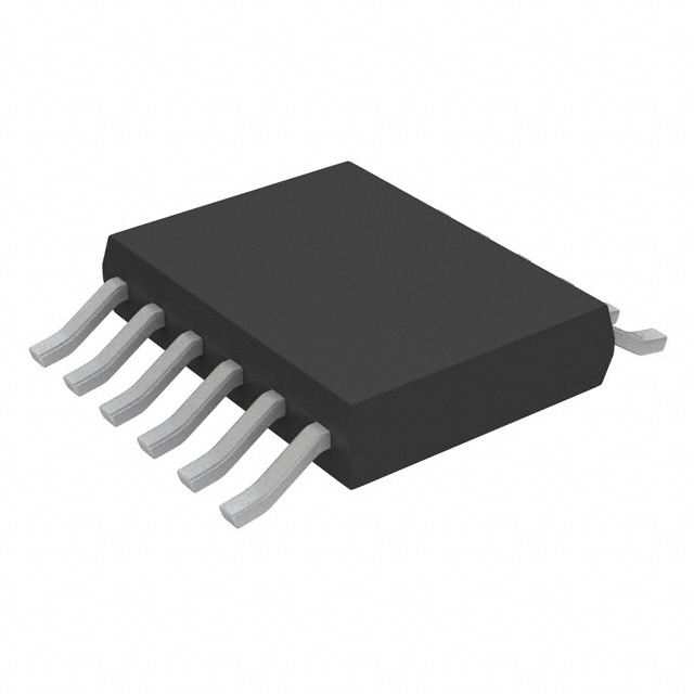
Ultra-Tiny, 12-Lead, 3mm × 3mm DFN and MSOP
Packages
The LTC®2461/LTC2463 are ultra tiny, 16-Bit analog-todigital converters with an integrated precision reference.
They use a single 2.7V to 5.5V supply and communicate
through an I2C Interface. The LTC2461 is single-ended
with a 0V to 1.25V input range and the LTC2463 is differential with a 1.25V input range. Both ADCs include a
1.25V integrated reference with 2ppm/°C drift performance and 0.1% initial accuracy. The converters are
available in a 12-pin 3mm × 3mm DFN package or an
MSOP-12 package. They include an integrated oscillator
and perform conversions with no latency for multiplexed
applications. The LTC2461/LTC2463 include a proprietary
input sampling scheme that reduces the average input
current several orders of magnitude when compared to
conventional delta sigma converters.
n
Following a single conversion, the LTC2461/LTC2463
automatically power down the converter and can also be
configured to power down the reference. When both the
ADC and reference are powered down, the supply current
is reduced to 200nA.
L, LT, LTC, LTM, Linear Technology and the Linear logo are registered trademarks of Linear
Technology Corporation. All other trademarks are the property of their respective owners.
Protected by U.S. Patents, including 6208279, 6411242, 7088280, 7164378.
The LTC2461/LTC2463 can sample at 60 conversions per
second and, due to the very large oversampling ratio,
have extremely relaxed antialiasing requirements. Both
include continuous internal offset and fullscale calibration
algorithms which are transparent to the user, ensuring accuracy over time and the operating temperature range.
APPLICATIONS
System Monitoring
Environmental Monitoring
n Direct Temperature Measurements
n Instrumentation
n Data Acquisition
n Embedded ADC Upgrades
n
TYPICAL APPLICATION
VREF vs Temperature
1.2520
0.1µF
0.1µF
0.1µF
10k
REFOUT
COMP VCC
IN+
10k
LTC2463
IN–
10k
R
0.1µF
SCL
SDA
REF–
10µF
0.1µF
A0
I2C
INTERFACE
GND
24613 TA01a
REFERENCE OUTPUT VOLTAGE (V)
2.7V TO 5.5V
1.2515
1.2510
1.2505
1.2500
1.2495
1.2490
1.2485
1.2480
–50
–30
–10 10
30
50
TEMPERATURE (°C)
70
90
24613 TA01b
24613fa
1
�LTC2461/LTC2463
ABSOLUTE MAXIMUM RATINGS
(Notes 1, 2)
Supply Voltage (VCC).................................... –0.3V to 6V
Analog Input Voltage
(VIN+, VIN –, VIN, VREF –,
VCOMP, VREFOUT )............................–0.3V to (VCC + 0.3V)
Digital Voltage
(VSDA, VSCL, VA0)...........................–0.3V to (VCC + 0.3V)
Storage Temperature Range................... –65°C to 150°C
Operating Temperature Range
LTC2461C/LTC2463C................................ 0°C to 70°C
LTC2461I/LTC2463I..............................–40°C to 85°C
PIN CONFIGURATION
LTC2463
LTC2463
TOP VIEW
REFOUT
1
12 VCC
COMP
2
11 GND
A0
GND
4
SCL
5
8 REF–
SDA
6
7 GND
10 IN
1
2
3
4
5
6
REFOUT
COMP
A0
GND
SCL
SDA
–
3
13
TOP VIEW
9 IN+
12
11
10
9
8
7
VCC
GND
IN–
IN+
REF–
GND
MS PACKAGE
12-LEAD PLASTIC MSOP
TJMAX = 125°C, θJA = 135°C/W
DD PACKAGE
12-LEAD (3mm × 3mm) PLASTIC DFN
TJMAX = 125°C, θJA = 43°C/W
EXPOSED PAD (PIN 13)
LTC2461
LTC2461
TOP VIEW
REFOUT
1
12 VCC
COMP
2
11 GND
10 GND
A0
3
GND
4
SCL
5
8 REF–
SDA
6
7 GND
13
TOP VIEW
REFOUT
COMP
A0
GND
SCL
SDA
9 IN
1
2
3
4
5
6
12
11
10
9
8
7
VCC
GND
GND
IN
REF–
GND
MS PACKAGE
12-LEAD PLASTIC MSOP
TJMAX = 125°C, θJA = 135°C/W
DD PACKAGE
12-LEAD (3mm × 3mm) PLASTIC DFN
TJMAX = 125°C, θJA = 43°C/W
EXPOSED PAD (PIN 13)
ORDER INFORMATION
LEAD FREE FINISH
TAPE AND REEL
PART MARKING*
PACKAGE DESCRIPTION
TEMPERATURE RANGE
LTC2461CDD#PBF
LTC2461CDD#TRPBF
LFGF
12-Lead Plastic (3mm × 3mm) DFN
0°C to 70°C
LTC2461IDD#PBF
LTC2461IDD#TRPBF
LFGF
12-Lead Plastic (3mm × 3mm) DFN
–40°C to 85°C
LTC2461CMS#PBF
LTC2461CMS#TRPBF
2461
12-Lead Plastic MSOP
0°C to 70°C
LTC2461IMS#PBF
LTC2461IMS#TRPBF
2461
12-Lead Plastic MSOP
–40°C to 85°C
LTC2463CDD#PBF
LTC2463CDD#TRPBF
LFGG
12-Lead Plastic (3mm × 3mm) DFN
0°C to 70°C
LTC2463IDD#PBF
LTC2463IDD#TRPBF
LFGG
12-Lead Plastic (3mm × 3mm) DFN
–40°C to 85°C
LTC2463CMS#PBF
LTC2463CMS#TRPBF
2463
12-Lead Plastic MSOP
0°C to 70°C
LTC2463IMS#PBF
LTC2463IMS#TRPBF
2463
12-Lead Plastic MSOP
–40°C to 85°C
Consult LTC Marketing for parts specified with wider operating temperature ranges. *The temperature grade is identified by a label on the shipping container.
Consult LTC Marketing for information on non-standard lead based finish parts.
For more information on lead free part marking, go to: http://www.linear.com/leadfree/
For more information on tape and reel specifications, go to: http://www.linear.com/tapeandreel/
24613fa
2
�LTC2461/LTC2463
ELECTRICAL CHARACTERISTICS
The l denotes the specifications which apply over the full operating
temperature range, otherwise specifications are at TA = 25°C. (Note 2)
PARAMETER
CONDITIONS
MIN
TYP
MAX
UNITS
16
Bits
Resolution (No Missing Codes)
(Note 3)
l
Integral Nonlinearity
(Note 4)
l
1
8
LSB
Offset Error
LTC2461, 30Hz, LTC2463
LTC2461, 60Hz
l
2
5
15
LSB
LSB
Offset Error Drift
0.02
LSB/°C
Gain Error
Includes Contributions of ADC and Internal Reference
l
±0.01
±0.25
% of FS
Gain Error Drift
Includes Contributions of ADC and Internal Reference
C-Grade
I-Grade
l
±2
±5
±10
ppm/°C
ppm/°C
Transition Noise
2.2
µVRMS
Power Supply Rejection DC
80
dB
The
ANALOG
INPUTS l denotes the specifications which apply over the full operating temperature range, otherwise
specifications are at TA = 25°C.
SYMBOL
PARAMETER
CONDITIONS
VIN
Positive Input Voltage Range
LTC2463
l
VIN–
Negative Input Voltage Range
LTC2463
l
Input Voltage Range
LTC2461
l
+
VIN
MIN
TYP
MAX
UNITS
0
VREF
V
0
VREF
V
0
VREF
V
+
Overrange/Underrange Voltage, IN+
VIN
– = 0.625V (See Figure 3)
8
LSB
VOR–, VUR–
Overrange/Underrange Voltage, IN–
VIN+ = 0.625V (See Figure 3)
8
LSB
CIN
IN+, IN–, IN Sampling Capacitance
+, V
VOR
UR
IDC_LEAK(IN+, IN–, IN) IN+, IN– DC Leakage Current (LTC2463)
IN DC Leakage Current (LTC2461)
0.35
VIN = GND or VCC (Note 8)
VIN = GND or VCC (Note 8)
pF
l
l
–10
–10
1
1
1.247
1.25
1.253
±2
±5
±10
ICONV
Input Sampling Current (Note 5)
VREF
REFOUT Output Voltage
l
REFOUT Voltage Temperature Coefficient (Note 9)
C-Grade
I-Grade
l
10
10
nA
nA
50
nA
V
ppm/°C
ppm/°C
Reference Line Regulation
2.7V ≤ VCC ≤ 5.5V
–90
dB
Reference Short Circuit Current
VCC = 5.5, Forcing REFOUT to GND
l
COMP Pin Short Circuit Current
VCC = 5.5, Forcing REFOUT to GND
l
Reference Load Regulation
2.7V ≤ VCC ≤ 5.5V, IOUT = 100μA Sourcing
3.5
mV/mA
Reference Output Noise Density
CCOMP= 0.1μF, CREFOUT = 0.1μF, At f = 1kHz
30
nV/√Hz
35
mA
200
µA
POWER REQUIREMENTS
The l denotes the specifications which apply over the full operating temperature
range, otherwise specifications are at TA = 25°C.
SYMBOL
PARAMETER
CONDITIONS
MIN
VCC
Supply Voltage
l
ICC
Supply Current
Conversion
Nap
Sleep
l
l
l
TYP
2.7
MAX
5.5
1.5
800
0.2
2.5
1500
2
UNITS
V
mA
µA
µA
24613fa
3
�LTC2461/LTC2463
2C INPUTS AND OUTPUTS
I The
l denotes the specifications which apply over the full operating temperature
range, otherwise specifications are at TA = 25°C. (Notes 2, 7)
SYMBOL
PARAMETER
VIH
High Level Input Voltage
CONDITIONS
l
MIN
VIL
Low Level Input Voltage
l
II
Digital Input Current
l
–10
0.05VCC
TYP
MAX
UNITS
0.7VCC
V
0.3VCC
V
10
µA
VHYS
Hysteresis of Schmidt Trigger Inputs
(Note 3)
l
VOL
Low Level Output Voltage (SDA)
I = 3mA
l
0.4
V
V
IIN
Input Leakage
0.1VCC ≤ VIN ≤ 0.9VCC
l
1
µA
CI
Capacitance for Each I/O Pin
l
CB
Capacitance Load for Each Bus Line
l
VIH(A0)
High Level Input Voltage for Address Pin
l
VIL(A0)
Low Level Input Voltage for Address Pin
l
10
pF
400
pF
0.95VCC
V
0.05VCC
V
2C TIMING CHARACTERISTICS
I The
l denotes the specifications which apply over the full operating
temperature range, otherwise specifications are at TA = 25°C. (Notes 2, 7)
SYMBOL
PARAMETER
CONDITIONS
tCONV
Conversion Time
l
MIN
TYP
MAX
UNITS
13
16.6
23
ms
400
kHz
fSCL
SCL Clock Frequency
l
0
tHD(SDA,STA)
Hold Time (Repeated) START Condition
l
0.6
ms
tLOW
LOW Period of the SCL Pin
l
1.3
ms
tHIGH
HIGH Period of the SCL Pin
l
0.6
ms
tSU(STA)
Set-Up Time for a Repeated START Condition
l
0.6
tHD(DAT)
Data Hold Time
l
0
tSU(DAT)
Data Set-Up Time
l
100
tr
Rise Time for SDA, SCL Signals
(Note 6)
l
20 + 0.1CB
300
tf
Fall Time for SDA, SCL Signals
(Note 6)
l
20 + 0.1CB
300
tSU(STO)
Set-Up Time for STOP Condition
l
0.6
ms
tBUF
Bus Free Time Between a Stop and Start Condition
l
1.3
ms
tOF
Output Fall Time VIHMIN to VILMAX
l
20 + 0.1CB
tSP
Input Spike Suppression
Note 1: Stresses beyond those listed under Absolute Maximum Ratings
may cause permanent damage to the device. Exposure to any Absolute
Maximum Rating condition for extended periods may affect device
reliability and lifetime.
Note 2: All voltage values are with respect to GND. VCC = 2.7V to 5.5V
unless otherwise specified.
Note 3: Guaranteed by design, not subject to test.
Note 4: Integral nonlinearity is defined as the deviation of a code from a
straight line passing through the actual endpoints of the transfer curve.
Guaranteed by design and test correlation.
Bus Load CB = 10pF to
400pF (Note 6)
l
ms
0.9
ms
ns
ns
ns
250
ns
50
ns
Note 5: Input sampling current is the average input current drawn from
the input sampling network while the LTC2461/LTC2463 are converting.
Note 6: CB = capacitance of one bus line in pF.
Note 7: All values refer to VIH(MIN) and VIL(MAX) levels.
Note 8: A positive current is flowing into the DUT pin.
Note 9: Voltage temperature coefficient is calculated by dividing the
maximum change in output voltage by the specified temperature range.
24613fa
4
�LTC2461/LTC2463
TYPICAL PERFORMANCE CHARACTERISTICS
Integral Nonlinearity (VCC = 5.5V)
Integral Nonlinearity (VCC = 2.7V)
3
TA = –45°C, 25°C, 90°C
TA = –45°C, 25°C, 90°C
2
1
1
1
0
INL (LSB)
2
0
–1
–1
–2
–2
–2
0.25
0.75
–0.75
–0.25
DIFFERENTIAL INPUT VOLTAGE (V)
–3
–1.25
1.25
0.25
0.75
–0.75
–0.25
DIFFERENTIAL INPUT VOLTAGE (V)
24613 G01
Offset Error vs Temperature
ADC Gain Error vs Temperature
Transition Noise vs Temperature
10
ADC GAIN ERROR (LSB)
VCC = 4.1V
1
VCC = 2.7V
0
–1
–2
15
10
VCC = 4.1V
5
–3
VCC = 2.7V
–4
–30
50
–10 10
30
TEMPERATURE (°C)
70
0
–50
90
0
25
50
TEMPERATURE (°C)
24613 G04
Conversion Mode Power Supply
Current vs Temperature
75
1.9
VCC = 4.1V
1.6
1.5
1.4
VCC = 2.7V
1.3
1.2
SLEEP CURRENT (nA)
1.7
50
–10 10
30
TEMPERATURE (°C)
70
4
VCC = 5.5V
250
200
150
VCC = 4.1V
100
90
24613 G07
0
–50
VCC = 2.7V
–30
50
–10 10
30
TEMPERATURE (°C)
VCC = 2.7V
3
2
1.2508
50
1.1
–30
5
VCC = 5.5V
–30
24613 G05
300
VCC = 5.5V
6
0
–50
100
350
1.8
7
Sleep Mode Power Supply
Current vs Temperature
2.0
1.0
–50
–25
8
1
REFERENCE OUTPUT VOLTAGE (V)
–5
–50
9
VCC = 5.5V
20
TRANSITION NOISE RMS (µV)
VCC = 5.5V
2
5 25 45 65 85 105 125
TEMPERATURE (°C)
24613 G03
25
3
OFFSET ERROR (LSB)
–3
–55 –35 –15
1.25
24613 G02
5
4
VCC = 5.5V, 4.1V, 2.7V
0
–1
–3
–1.25
CONVERSION CURRENT (mA)
INL vs Temperature
3
2
INL (LSB)
INL (LSB)
3
(TA = 25°C, unless otherwise noted)
70
90
24613 G08
50
–10 10
30
TEMPERATURE (°C)
70
90
24613 G06
VREF vs Temperature
VCC = 5V
1.2507
1.2506
1.2505
1.2504
1.2503
1.2502
–50
–30
50
–10 10
30
TEMPERATURE (°C)
70
90
24613 G09
24613fa
5
�LTC2461/LTC2463
TYPICAL PERFORMANCE CHARACTERISTICS
CONVERSION TIME (ms)
–20
REJECTION (dB)
Conversion Time vs Temperature
TA = 25°C
VCC = 4.1V
–40
–60
–80
–100
–120
21
1.24892
20
1.24891
VCC = 5V, 4.1V, 3V
18
17
10
100 1k 10k 100k
FREQUENCY AT VCC (Hz)
1M
14
–50
10M
24613 G10
TA = 25°C
1.24889
1.24888
1.24887
16
1.24886
15
1
VREF vs VCC
1.24890
19
VREF (V)
0
Power Supply Rejection
vs Frequency at VCC
(TA = 25°C, unless otherwise noted)
1.24885
–25
25
50
0
TEMPERATURE (°C)
75
100
24613 G11
1.24884
2.0
2.5
3.0
3.5
4.0 4.5
VCC (V)
5.0
5.5
6.0
24613 G12
PIN FUNCTIONS
REFOUT (Pin 1): Reference Output Pin. Nominally 1.25V,
this voltage sets the fullscale input range of the ADC. For
noise and reference stability connect to a 0.1µF capacitor
tied to GND. This capacitor value must be less than or
equal to the capacitor tied to the reference compensation
pin (COMP). REFOUT cannot be overdriven by an external
reference. For applications that require an input range
greater than 0V to 1.25V, please refer to the LTC2451/
LTC2453.
COMP (Pin 2): Internal Reference Compensation Pin. For
low noise and reference stability, tie a 0.1μF capacitor to
GND.
A0 (Pin 3): Chip Address Control Pin. The A0 pin can be
tied to GND or VCC. If A0 is tied to GND, the LTC2461/
LTC2463 I2C address is 0010100. If A0 is tied to VCC, the
LTC2461/LTC2463 I2C address is 1010100.
GND (Pins 4, 7, 11): Ground. Connect directly to the
ground plane through a low impedance connection.
I 2C
Interface. The
SCL (Pin 5): Serial Clock Input of the
LTC2461/LTC2463 can only act as a slave and the SCL pin
only accepts external serial clock. Data is shifted into the
SDA pin on the rising edges of SCL and output through
the SDA pin on the falling edges of SCL.
SDA (Pin 6): Bidirectional Serial Data Line of the I2C Interface. The conversion result is output through the SDA pin.
The pin is high impedance unless the LTC2461/LTC2463
is in the data output mode. While the LTC2461/LTC2463
is in the data output mode, SDA is an open drain pull
down (which requires an external 1.7k pull-up resistor
to VCC).
REF– (Pin 8): Negative Reference Input to the ADC. The
voltage on this pin sets the zero input to the ADC. This
pin should tie directly to ground or the ground sense of
the input sensor.
IN+ (LTC2463), IN (LTC2461) (Pin 9): Positive input voltage for the LTC2463 differential device. ADC input for the
LTC2461 single-ended device.
IN– (LTC2463), GND (LTC2461) (Pin 10): Negative input
voltage for the LTC2463 differential device. GND for the
LTC2461 single-ended device.
VCC (Pin 12): Positive Supply Voltage. Bypass to GND with
a 10μF capacitor in parallel with a low-series-inductance
0.1μF capacitor located as close to pin 12 as possible.
Exposed Pad (Pin 13 – DFN Package): Ground. Connect
directly to the ground plane through a low impedance
connection.
24613fa
6
�LTC2461/LTC2463
BLOCK DIAGRAM
1
9
10
IN+
(IN)
IN–
(GND)
2
REFOUT
COMP
INTERNAL
REFERENCE
∆Σ A/D
CONVERTER
12
VCC
A0
I2C
INTERFACE
SCL
SDA
DECIMATING
SINC FILTER
–
3
5
6
∆Σ A/D
CONVERTER
INTERNAL
OSCILLATOR
8
REF–
4, 7, 11, 13 (DD PACKAGE)
GND
24613 BD
( ) PARENTHESIS INDICATE LTC2461
Figure 1. Functional Block Diagram
APPLICATIONS INFORMATION
CONVERTER OPERATION
POWER-ON RESET
Converter Operation Cycle
The LTC2461/LTC2463 are low power, delta sigma, analog to digital converters with a simple I2C interface (see
Figure 1). The LTC2463 has a fully differential input while
the LTC2461 is single-ended. Both are pin and software
compatible. Their operation is composed of three distinct
states: CONVERT, SLEEP/NAP, and DATA INPUT/OUTPUT
(see Figure 2). The operation begins with the CONVERT
state. Once the conversion is finished, the converter automatically powers down (NAP) or, under user control, both
the converter and reference are powered down (SLEEP).
The conversion result is held in a static register while the
device is in this state. The cycle concludes with the DATA
INPUT/OUTPUT state. Once all 16-bits are read the device
begins a new conversion.
The CONVERT state duration is determined by the LTC2461/
LTC2463 conversion time (nominally 16.6 milliseconds).
Once started, this operation can not be aborted except by a
low power supply condition (VCC < 2.1V) which generates
an internal power-on reset signal.
After the completion of a conversion, the LTC2461/LTC2463
enters the SLEEP/NAP state and remains there until a valid
CONVERT
SLEEP/NAP
NO
READ/WRITE
ACKNOWLEDGE
YES
DATA INPUT/OUTPUT
NO
STOP
OR
READ 16 BITS
YES
24613 F02
Figure 2. LTC2461/LTC2463 State Transition Diagram
read/write is acknowledged. Following this condition, the
ADC transitions into the DATA INPUT/OUTPUT state.
While in the SLEEP/NAP state, the LTC2461/LTC2463’s
converters are powered down. This reduces the supply
24613fa
7
�LTC2461/LTC2463
APPLICATIONS INFORMATION
current by approximately 50%. While in the Nap state,
the reference remains powered up. To power down the
reference in addition to the converter, the user can select
the SLEEP mode during the DATA INPUT/OUTPUT state.
Once the next conversion is complete, SLEEP state is
entered and power is reduced to 200nA. The reference
is powered up once a valid read/write is acknowledged.
The reference startup time is 12ms (if the reference and
compensation capacitor values are both 0.1μF).
Power-Up Sequence
When the power supply voltage (VCC) applied to the converter is below approximately 2.1V, the ADC performs a
power-on reset. This feature guarantees the integrity of
the conversion result.
When VCC rises above this critical threshold, the converter
generates an internal power-on reset (POR) signal for
approximately 0.5ms. The POR signal clears all internal
registers. Following the POR signal, the LTC2461/LTC2463
start a conversion cycle and follow the succession of states
shown in Figure 2. The reference startup time following a
POR is 12ms (CCOMP = CREFOUT = 0.1μF). The first conversion following power-up will be invalid since the reference
voltage has not completely settled. The first conversion
following power up can be discarded using the data abort
command or simply read and ignored. The following conversions are accurate to the device specifications.
The LTC2461/LTC2463 perform offset calibrations every
conversion cycle. This calibration is transparent to the
user and has no effect upon the cyclic operation described
previously. The advantage of continuous calibration is
stability of the ADC performance with respect to time and
temperature.
The LTC2461/LTC2463 include a proprietary input sampling
scheme that reduces the average input current by several
orders of magnitude when compared to traditional deltasigma architectures. This allows external filter networks
to interface directly to the LTC2461/LTC2463. Since the
average input sampling current is 50nA, an external RC
lowpass filter using 1kΩ and 0.1µF results in