LTC2928
Multichannel Power Supply
Sequencer and Supervisor
Description
Features
Easily Configure Power Management
without Software
nn Controls Up to Four Supplies per Device
nn Cascades for Additional Supplies
nn Staged Supply Sequencing with
Adjustable Time Positions
nn Fault Event Reporting with Diagnostics
nn Selectable System Shutdown on Fault
nn 1.5% Undervoltage Monitor Accuracy
nn Overvoltage and/or Fault Indication
nn Configurable Undervoltage and
Overvoltage Thresholds
nn Charge Pumped Enable Pins Drive N-Channel MOSFETs
nn Operates from 2.9V to 16.5V
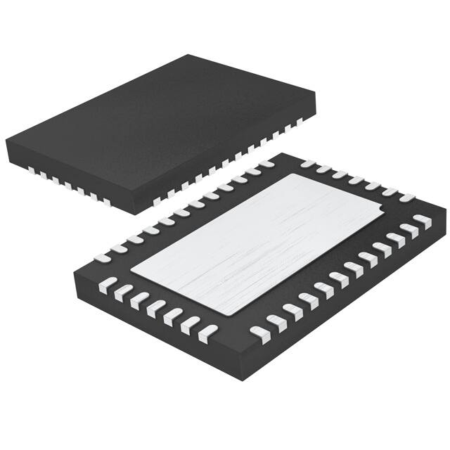
nn 5mm × 7mm 38-lead QFN and
36-lead SSOP Packages
The LTC®2928 is a four channel cascadable power
supply sequencer and high accuracy supervisor. Sequencing thresholds, order and timing are configured with just a
few external components, negating the need for PC board
layout or software changes during system development.
Multiple LTC2928s may be easily connected to sequence
an unlimited number of power supplies.
nn
Sequence outputs control supply enable pins or
N-channel pass gates. Precision input comparators with
individual outputs monitor power supply voltages to 1.5%
accuracy. Supervisory functions include undervoltage
and overvoltage monitoring and reporting as well as µP
reset generation. RST may be forced high to complement
margin testing.
Application faults, whether internally or externally generated, can shut down all controlled supplies. The type and
source of faults are reported for diagnosis. Individual
channel controls are available to independently exercise
enable outputs and supervisory functions.
Applications
Network/Telecom Infrastructure
Sequencing for Multiple I/O and Core Voltages
nn Power Management
nn
A high voltage input allows the LTC2928 to be powered
from voltages as high as 16.5V. A buffered reference
output permits single negative power supply sequencing
and monitoring operations.
nn
L, LT, LTC, LTM, Linear Technology and the Linear logo are registered trademarks of Linear
Technology Corporation. All other trademarks are the property of their respective owners.
Protected by U.S. Patents, including 4843302, 6949965.
Typical Application
12V
VIN
3.3V
RUN
10k
VIN
Si7894ADP
1µF
1.8V
1V/DIV
ON
AXA010AY93
95.3k
24.3k
9.53k
1.5k
3.4k
3.3V
2.5V
1.8V
1.2V
1.2V
2.5V
AUSTIN LYNX
VIN
VOUT
ON
LTC3414
VOUT
RUN
LTC1628
VIN
VOUT
RUN
0.1µF
Sequencing Up and Down
LTM4600
VOUT
100Ω
HVCC
EN2
ON
RT1
RT2
RT3
RT4
DONE
VCC
GND MS1 VSEL
EN1 EN4
12.1k
36.5k
23.2k
EN3
51.1k
V1
V2
V3
LTC2928
V4
RST
OV
FLT
RTMR PTMR STMR
0.047µF
ALL RESISTORS 1%
DONE
SYSTEM
RESET
FAULT
3300pF
10k
10k
10k
10k
2928 TA06
For more information www.linear.com/LTC2928
START
SEQUENCE SEQUENCE UP
START
UP COMPLETE
SEQUENCE
DOWN
SEQUENCE
DOWN
COMPLETE
2928 TA07
2928fa
1
�LTC2928
Absolute Maximum Ratings
(Note 1)
Supply Voltages
HVCC....................................................... –0.3V to 18V
VCC........................................................ –0.3V to 6.5V
Input Voltages
V1, V2, V3, V4..........................................–0.3V to 12V
MS1, MS2, RDIS.................................... –0.3V to 6.5V
SQT1, SQT2, VSEL ................................ –0.3V to 6.5V
RT1, RT2, RT3, RT4............................... –0.3V to 6.5V
ON, OVA..........................................–0.3 to VCC + 0.3V
STMR, PTMR, RTMR......................–0.3 to VCC + 0.3V
Output Voltages
EN1, EN2, EN3, EN4 (Note 3)...................–0.3V to 12V
CMP1, CMP2, CMP3, CMP4.................. –0.3V to 6.5V
FLT, RST, OV, CAS................................. –0.3V to 6.5V
DONE, REF....................................–0.3V to VCC + 0.3V
RMS Currents
IVCC.................................................................. ±10mA
IHVCC............................................................... ±20mA
IREF................................................................... ±10mA
Operating Ambient Temperature Range
LTC2928C................................................. 0°C to 70°C
LTC2928I..............................................–40°C to 85°C
Storage Temperature Range
SSOP Package.................................... –65°C to 150°C
QFN Package...................................... –65°C to 150°C
Lead Temperature (Soldering, 10 sec)
SSOP Package................................................... 300°C
Pin Configuration
TOP VIEW
V2
4
33 EN3
OVA 1
31 EN3
OVA
5
32 V4
EN1 2
30 V4
EN1
6
31 EN4
V1 3
29 EN4
V1
7
30 RTMR
N/C 4
28 RTMR
29 PTMR
REF 5
27 PTMR
28 STMR
RT1 6
RT2 10
27 VSEL
RT2 7
RT3 11
26 GND
RT4 12
25 HVCC
22 OV
MS2 16
21 FLT
RDIS 17
20 DONE
CAS 18
22 VCC
SQT2 11
21 RST
13 14 15 16 17 18 19
UHF PACKAGE
38-LEAD (5mm × 7mm) PLASTIC QFN
19 ON
G PACKAGE
36-LEAD PLASTIC SSOP
TJMAX = 125°C, θJA = 95°C/W
20 OV
MS1 12
FLT
MS1 15
SQT1 10
DONE
23 RST
23 HVCC
N/C
SQT2 14
24 GND
RT4 9
ON
24 VCC
25 VSEL
RT3 8
CAS
SQT1 13
26 STMR
39
MS2
9
38 37 36 35 34 33 32
RDIS
RT1
8
V3
34 V3
CMP3
EN2
CMP4
35 CMP3
3
CMP1
2
CMP2
CMP2
EN2
36 CMP4
V2
1
REF
2
TOP VIEW
CMP1
TJMAX = 125°C, θJA = 34°C/W
EXPOSED PAD (PIN 39) PCB GND CONNECTION OPTIONAL
2928fa
For more information www.linear.com/LTC2928
�LTC2928
Order Information
LEAD FREE FINISH
TAPE AND REEL
PART MARKING
PACKAGE DESCRIPTION
TEMPERATURE RANGE
LTC2928CG#PBF
LTC2928CG#TRPBF
LTC2928CG
36-Lead Plastic SSOP (5.3mm)
0°C to 70°C
LTC2928IG#PBF
LTC2928IG#TRPBF
LTC2928IG
36-Lead Plastic SSOP (5.3mm)
0°C to 70°C
LTC2928CUHF#PBF
LTC2928CUHF#TRPBF
LTC2928CUHF
38-Lead (5mm × 7mm) Plastic QFN
–40°C to 85°C
LTC2928IUHF#PBF
LTC2928IUHF#TRPBF
LTC2928IUHF
38-Lead (5mm × 7mm) Plastic QFN
–40°C to 85°C
Consult LTC Marketing for parts specified with wider operating temperature ranges.
For more information on lead free part marking, go to: http://www.linear.com/leadfree/
For more information on tape and reel specifications, go to: http://www.linear.com/tapeandreel/
Electrical Characteristics
The l denotes the specifications which apply over the full operating
temperature range, otherwise specifications are at TA = 25°C, VCC = 3.3V unless otherwise noted.
SYMBOL
PARAMETER
CONDITIONS
MIN
TYP
MAX
UNITS
Supply Pins: VCC, HVCC
VVCC
VCC Input Supply Range
l
2.9
6
V
IVCC
VCC Input Supply Current
HVCC = GND
l
1
2.5
mA
VUVL
VCC Input Supply Undervoltage Lockout
VCC Rising
l
2.75
2.8
2.85
V
VUVL(HYST)
Undervoltage Lockout Hysteresis
l
50
100
150
mV
VHVCC
High Voltage Input Supply Range
l
7.2
12
16.5
V
VCC(REG)
Regulated VCC from HVCC
l
3.2
3.3
3.4
V
IREG
Regulated VCC Output Current to
External Load (Note 2)
–10
mA
IHVCC
HVCC Input Supply Current
1
2
mA
VHVCC = 12V
l
IREG = 0mA, VHVCC = 12V
l
VON Rising
l
0.985
1.00
1.015
l
20
30
40
mV
±50
nA
Sequence Up/Down Pin: ON
VON
ON Threshold Voltage
VON(HYST)
ON Hysteresis
ION(LKG)
ON Leakage Current
V
VON = 1V
l
VSEL = VCC
l
l
0.4925
0.500
0.5075
±18
V
mV
l
l
l
0.315
0.149
0.032
0.333
0.167
0.05
0.351
0.185
0.068
V
V
V
±15
nA
Voltage Monitor Pins: V1, V2, V3, V4
VMON(TH)
Reset Threshold Voltage
V1 Negative Threshold Voltage
VSEQ(TH)
Sequencing Thresholds
0.67 VMON(TH)
0.33 VMON(TH)
0.10 VMON(TH)
See Table 4
IMON(LKG)
Monitor Pin Leakage Current
VMON = 0.55V
tMON(UV)
Undervoltage Pulse Width Required to
Trip Comparators
VMON below VMON(TH) by 1%
225
µs
tMON(OV)
Overvoltage Pulse Width Required to
Trip OV
VMON above Overvoltage Threshold by
1%
225
µs
l
2928fa
For more information www.linear.com/LTC2928
3
�LTC2928
Electrical Characteristics
The l denotes the specifications which apply over the full operating
temperature range, otherwise specifications are at TA = 25°C, VCC = 3.3V unless otherwise noted.
SYMBOL
PARAMETER
CONDITIONS
MIN
TYP
MAX
UNITS
Supply Enable Pins: EN1, EN2, EN3, EN4
VEN
Enable Pin Voltage Output in On State
IEN = –1µA
l
VCC + 4.5
VCC +
5.5
VCC + 6
V
IEN(UP)
Enable Pin Pull-Up Current
Enable Pin On, VEN ≤ (VCC + 4V)
l
–7.5
–10
–12.5
µA
VEN(OL)
Enable Pin Voltage Output Low
IEN = 2.5mA
l
0.25
0.4
V
0.15
0.3
V
Comparator Outputs: CMP1, CMP2, CMP3, CMP4
VCMP(OL)
Comparator Voltage Output Low
ICMP = 2.5mA
l
VCMP(OH)
Comparator Voltage Output High
(Note 4)
ICMP = –1µA
l
VCC – 1
V
Three-State Selection Inputs: SQT1, SQT2, MS1, MS2, RDIS
VIL
Voltage Input Low Threshold
l
VIH
Voltage Input High Threshold
l
1.4
V
IHZ
High Z Pin Current
l
l
–10
10
µA
µA
VHZ = 0.7V
VHZ = 1.1V
0.4
V
Positive/Negative Selection Input: VSEL
VIL
Voltage Input Low Threshold
l
VIH
Voltage Input High Threshold
l
0.4
1.4
V
V
Sequence Time Position Control Inputs: RT1, RT2, RT3, RT4 (see resistor selection Table 3)
VRT(LO)
Voltage Required to Force Enable Pin
Low While Sequencing
l
0.045 • VCC
VRT(HI)
Voltage Required to Force Enable Pin
High Outside of Sequencing
l 0.955 • VCC
RRT
RT Pin Input Resistance
l
11.2
V
V
12
12.8
kΩ
0.15
0.3
V
Cascade Pin: CAS
VCAS(OL)
CAS Voltage Output Low
ICAS = 2.5mA
l
ICAS(UP)
CAS Pull-Up Current
Master Pulling CAS High, VCAS = GND
l
–45
–60
–75
µA
tCAS(HI)
Fixed Time Delay between Sequence
Time Positions (Note 5)
CAS High, CSTMR = 1500pF
l
11
13
15
ms
tCAS(MIN)
Minimum CAS Low Time During
Sequencing
l
15
22.5
30
µs
0.15
0.3
V
Fault Status Pin: FLT
VFLT(OL)
FLT Voltage Output Low
IFLT = 2.5mA
l
IFLT(UP)
FLT Pull-Up Current
VFLT = VCC –1V
l
–12
–17
–22
µA
VFLT(TH)
External Fault Input Threshold
VFLT Falling
l
1.0
1.1
1.2
V
VFLT(HYST)
External Fault Input Hysteresis
l
25
100
150
mV
tFLT
Minimum Detectable External Fault
Pulse Width
2
µs
IFLT(LKG)
Fault Pin Leakage Current
±1
µA
0.3
V
VFLT = VCC
l
IDONE = 2.5mA
l
Done Status Pin: DONE
VDONE(OL)
4
DONE Voltage Output Low
0.15
2928fa
For more information www.linear.com/LTC2928
�LTC2928
Electrical Characteristics
The l denotes the specifications which apply over the full operating
temperature range, otherwise specifications are at TA = 25°C, VCC = 3.3V unless otherwise noted.
SYMBOL
PARAMETER
CONDITIONS
IDONE(DN)
DONE Pull-Down Current
VDONE = 3.3V (Note 6)
l
MIN
RDONE
Required Pull-Up Resistance on “Last”
LTC2928
5% Tolerance or Better
l
2.4
VDONE(LAST)
Voltage Output High when Configured
as “Last”
l
0.8 • VCC
TYP
20
MAX
UNITS
40
µA
5.1
kΩ
V
Reset Pin: RST
VRST(OL)
RST Voltage Output Low
VCC = 0.2V, IRST = 0.1µA
VCC = 0.5V, IRST = 5µA
VCC = 1V, IRST = 200µA
VCC = 3V, IRST = 2500µA
l
l
l
l
5
10
25
150
VRST(OH)
RST Voltage Output High
IRST = –1µA (Note 7)
l
VCC – 1
60
150
300
300
mV
mV
mV
mV
V
Timer Pins: RTMR, PTMR, STMR
ITMR(UP)
Timer Pull-Up Current
VTMR = GND
l
–1.7
–2
–2.3
µA
ITMR(DN)
Timer Pull-Down Current
VTMR = 1.3V
l
15
20
25
µA
tRTMR
tPTMR
tSTMR
Timer Period, RTMR (Note 8)
Timer Period, PTMR
Timer Period, STMR
CRTMR = 1500pF
CPTMR = 1500pF
CSTMR = 1500pF
l
l
l
5
5
11
6
6
13
7
7
15
ms
ms
ms
IREF = 0.2mA, –1mA, CREF = ≤ 1000pF
VSEL = VCC
VSEL = VCC
VSEL = VCC
VSEL = VCC
l
l
l
l
l
1.172
1.172
0.780
0.386
0.109
1.189
1.189
0.793
0.396
0.119
1.205
1.205
0.806
0.406
0.129
0.15
0.3
External Voltage Reference Pin: REF
VREF
Reference Voltage Output
100% Sequence Threshold
67% Sequence Threshold
33% Sequence Threshold
10% Sequence Threshold
V
V
V
V
V
Over Voltage Indication Pin: OV
VOV(OL)
OV Voltage Output Low
IOV = 2.5mA
l
VOV(OH)
OV Voltage Output High (Note 7)
IOV = –1mA
l
VCC – 1
V
tOV
OV Indication Time (Note 8)
OV Low Time Upon Cleared
OV Event, CRTMR = 1500pF
l
5
6
7
VOVA = GND
l
0.546
0.556
0.566
V
VOVA Floating
VOVA = VCC = 3.3V
l
l
0.650
1.042
0.660
1.072
0.670
1.102
V
V
V
ms
Over Voltage Adjust Pin: OVA
VOVA(TH)
Over Voltage Threshold at Comparator
Inputs (Note 9)
Note 1: Stresses beyond those listed under Absolute Maximum Ratings
may cause permanent damage to the device. Exposure to any Absolute
Maximum Rating condition for extended periods may affect device
reliability and lifetime.
Note 2: All currents into pins are positive, all voltages are referenced to
GND unless otherwise noted.
Note 3: Internal circuits regulate the EN output voltage to VEN. Driving this
pin to voltages beyond VEN may damage the part.
Note 4: The comparator outputs have internal pull-ups to VCC of typically
–10µA. However, external pull-up resistors may be used when faster rise
times are required or for VOH voltages greater than VCC.
Note 5: The CAS high time after an ON edge is stretched by the ON pin
propagation delay (20µs typical).
Note 6: The DONE pull-down current is present when DONE is high to
facilitate cascading multiple LTC2928s.
Note 7: The RST and OV outputs have an internal pull-up to VCC of
typically –10µA. However, external pull-up resistors may be used when
faster rise times are required or for VOH voltages greater than VCC.
Note 8: If the termination of under and overvoltage events occur within
one nominal tRTMR period, the variation in tRTMR and/or tOV may be ±15%.
Note 9: Use a resistor from OVA to ground or VCC to configure overvoltage
thresholds within the max/min ranges shown. See Applications
Information for details.
2928fa
For more information www.linear.com/LTC2928
5
�LTC2928
Typical Performance Characteristics
IVCC vs VCC
1
HVCC = GND
85°C
4
IHVCC vs HVCC
3.4
IREG = 0
0.95
85°C
REGULATED VCC (V)
5
25°C
IHVCC (mA)
IVCC (mA)
3
–40°C
2
0.9
25°C
0.85
–40°C
1
0
3.4
0.8
2.5
3
3.5
4
4.5
VCC (V)
5
5.5
0.75
6
9
7
11
13
HVCC (V)
2928 G08
Regulated VCC vs HVCC
3.4
IREG = 0
15
Regulated VCC vs Temperature
IREG = 0
3.35
HVCC = 7.2V
3.3
HVCC = 16.5V
3.25
HVCC = 12V
3.2
–50
17
–25
2928 G09
Regulated VCC vs IREG
12
HVCC = 12V
0
25
50
TEMPERATURE (°C)
75
100
2928 G10
Enable Output Voltage in
On State vs VCC
10
3.3
3.25
3.35
8
–40°C
25°C
3.3
VEN (V)
REGULATED VCC (V)
VCC (V)
3.35
85°C
6
4
3.25
2
7
9
11
13
HVCC (V)
15
3.2
17
0
–10
1
0
2928 G12
2
3
VCC (V)
4
5
6
2928 G13
V1 Negative Threshold vs
Temperature
18
0.506
VSEL = VCC
12
0.504
VCC = 3V
VMON(TH) (mV)
VEN (V)
–8
0.508
VCC = 6V
8
6
4
0.502
0.5
0.498
6
0
–6
0.496
2
6
–4
–6
IREG (mA)
Under Voltage Monitor Threshold
(100%) vs Temperature
10
0
–2
2928 G11
Enable Output Voltage vs Enable
Output Current and VCC
12
0
VMON(TH) (mV)
3.2
–12
0.494
0
–2
–4
–6
IEN (µA)
–8
–10
–12
2928 G14
0.492
–50
–25
0
25
50
TEMPERATURE (°C)
75
100
2928 G07
–18
–50
–25
0
25
50
TEMPERATURE (°C)
75
100
2928 G06
2928fa
For more information www.linear.com/LTC2928
�LTC2928
Typical Performance Characteristics
Reference Output Voltage vs
Temperature
Comparator Under-Voltage
Glitch Immunity
Comparator Over-Voltage
Glitch Immunity
1k
1k
1.200
1.192
1.188
GLITCH DURATION (µs)
GLITCH DURATION (µs)
VREF (V)
1.196
RESET OCCURS
ABOVE CURVE
100
COMPARATOR
IGNORES GLITCH
OV OCCURS
ABOVE CURVE
100
COMPARATOR
IGNORES GLITCH
1.184
1.180
–50
–25
0
25
50
TEMPERATURE (°C)
75
10
100
1
10
COMPARATOR OVERDRIVE
(% OF RESET THRESHOLD)
0.1
2928 G05
10
100
1
10
COMPARATOR OVERDRIVE
(% OF OV THRESHOLD)
0.1
100
2928 G16
2928 G15
Relative Reset Output Voltage vs
VCC (with Reset Pull-Up Resistor
to VCC)
ON Threshold Voltage (Rising) vs
Temperature
1.015
RST Pull-Up Current vs
External Voltage on RST
50
–70
1k
1.010
40
1.000
0.995
–50
30
5k
20
–30
10k
10
–25
0
25
50
TEMPERATURE (°C)
75
100k
VCC = 3.3V
0
0.1
100
2928 G01
0.3
–10
0.5
0.7 0.9
VCC (V)
1.1
0
1.5
1.3
Three State Selection Pin Current
vs Pin Voltage
(SQT1, SQT2, MS1, MS2, RDIS)
Sequence, Reset and Power-Good
Timing vs Capacitance
–22
20
THREE STATE PIN CURRENT (µA)
10
1
SEQUENCER TIMER
100m
10m
RESET AND
POWER-GOOD TIMER
1m
10p
10n
100p1n
CAPACITANCE (F)
100n
1µ
0
1
2928 G17
2
3
VRST (V)
5
4
2928 G17
IFLT(UP) vs Temperature
15
VFLT = 2.3V
–20
10
5
IFLT(UP) (µA)
0.985
–50
TIME (SEC)
–40
–20
0.990
100m
IRST (µA)
VRST (% OF VCC)
VON (V)
1.005
VCC = 5V
–60
0
–5
–10
–18
–16
–14
–15
–20
0.3
0.6
0.9
1.2
THREE STATE PIN VOLTAGE (V)
1.5
2928 G20
–12
–50
–25
0
25
50
TEMPERATURE (°C)
75
100
2928 G21
2928 G19
2928fa
For more information www.linear.com/LTC2928
7
�LTC2928
Typical Performance Characteristics
–75
ICAS(UP) vs Temperature
(device configured as MASTER)
VCAS = GND
85°C
–57
25°C
0
25
50
TEMPERATURE (°C)
75
0
100
Voltage Output Low vs IOL
(CMP, CAS, FLT, DONE, RST, OV)
–45°C
0.5
0
5
1.5
25°C
1.25
–45°C
1
0.75
0.25
20
0
25
5
10
15
IOL (mA)
20
VOL = 0.4V
4
1.25
85°C
1
25°C
0.75
0
25
VOL = 0.2V
2
–45°C
0.5
3
1
0
5
10
15
IOL (mA)
20
0
25
0
VOL = 0.2V
6
4
4
2
2
3
VCC (V)
8
IRST (mA)
8
ICMP (mA)
8
2
4
3
VCC (V)
4
5
6
2928 G27
VOL = 0.4V
10
1
2
Reset Current Sink Capability vs
VCC and VOL
12
10
0
1
2928 G26
VOL = 0.4V
0
25
2928 G24
5
2928 G25
6
20
1.5
Comparator Output Current Sink
Capability vs VCC and VOL
12
10
15
IEN (mA)
Enable Current Sink Capability vs
VCC and VOL
6
0.25
0
5
0
2928 G23
VCC = 5V
1.75
85°C
10
15
IEN (mA)
Voltage Output Low vs IOL
(CMP, CAS, FLT, DONE, RST, OV)
2
VCC = 3.3V
25°C
1.5
1
2928 G22
1.75
0
2
IEN (mA)
–25
VOLTAGE OUTPUT LOW (V)
2
–45°C
1.5
0.5
–45
–50
85°C
2.5
1
–51
VCC = 5V
3
VEN(OL) (V)
–63
VEN(OL) vs IEN
3.5
2
VEN(OL) (V)
ICAS(UP) (µA)
VCC = 3.3V
2.5
–69
VOLTAGE OUTPUT LOW (V)
VEN(OL) vs IEN
3
5
6
0
VOL = 0.2V
0
2928 G28
1
2
3
VCC (V)
4
5
6
2928 G29
2928fa
For more information www.linear.com/LTC2928
�LTC2928
Pin Functions
CAS: Cascade Input/Output. Connect the cascade pin between a master and one or more slave devices to increase
the number of supplies that can be sequenced per time
position. See Applications Information for details. Do not
add capacitance to the cascade pin. Leave open if unused.
CMP1-CMP4: Comparator and/or Fault Status Outputs.
The CMP outputs have a weak internal pull-up to VCC and
may be pulled above VCC using an external pull-up. During
sequence-up or sequence-down operation, all comparator outputs are low. After sequencing-up, during supply
monitoring, comparator outputs pull low if their monitor
input drops below its undervoltage threshold. In the event
of a system fault, the CMP outputs latch and may be read
to diagnose the type and source of fault. See Applications
Information for the fault reporting details. Leave the CMP
outputs open if unused.
DONE: Sequence Done Output. The last (or only)
LTC2928 must have DONE pulled high with an external
resistor to VCC (3.3k 5% recommended). The LTC2928
floats DONE until the completion of a sequence-up
operation when it is pulled down. At the end of a
sequence-down operation, the LTC2928 returns DONE
to a high-impedance state. If subsequent time positions
are required for additional supplies, use the DONE—ON
handshake connection. See Applications Information
regarding the DONE—ON protocol.
EN1-EN4: Enable Outputs. Connect these outputs to a power
supply shutdown input or an external N-channel MOSFET
gate for the supply to be sequenced. When enabled, each
output is connected to an internal charge pumped supply (nominally VCC + 5.5V) via an internal 10µA current
source. When disabled, each output is pulled to ground.
EN outputs operate with their respective RT inputs. Leave
enable outputs open when unused.
Exposed Pad: Exposed pad may be left floating or connected to device ground.
FLT: Fault Input/Output. Pull FLT high with an external
resistor (10k recommended). The LTC2928 will pull FLT
low if an internal fault condition is detected (see Applications Information for details). An external signal such as
OV may also pull down the FLT pin to cause an external
fault. Any internal or external fault condition forces all
enable outputs low. In order to clear a fault condition, a
“return-to-zero” state must be reached with all monitored
supplies falling below their configured sequence-down
thresholds, while the ON input is below 0.97V. Debugging
modes are available (use the MS1, MS2 inputs) to leave
supplies enabled upon system faults. See Applications
Information for configuration tables.
GND: Device ground.
HVCC: High Voltage (7.2V to 16.5V) Power Supply Input.
Bypass HVCC with at least 0.1µF to ground in close proximity to this pin. The internal HVCC regulator provides a
regulated 3.3V to VCC. VCC may be used to power external circuits (limited to 10 mA external load). Tie HVCC to
ground when unused.
MS1, MS2: Master/Slave Three State Configuration Inputs. Depending on the application, select each LTC2928
as a master or slave part and whether or not the part is
designated as the first part in a cascade application. The
RST—FLT relationship (after RST pulls high for the first
time) is also configured with these inputs. Select whether
or not RST pulling low should cause FLT to pull low and
shutdown the system. Select debugging modes to leave
supplies enabled upon system faults. See Applications
Information for configuration table.
N/C: No Connect. Unconnected pins.
ON: Sequence Up/Down Input. A voltage transition above
1V starts the sequence-up phase. A voltage transition below
0.97V starts the sequence-down phase. An ON transition
applied during a sequence-up (or down) phase is treated
as a command fault. See Applications Information for using the DONE—ON handshake protocol when cascading
multiple LTC2928s to append additional time positions.
2928fa
For more information www.linear.com/LTC2928
9
�LTC2928
Pin Functions
OV: Overvoltage Output. Pulls low when any positive supply
exceeds its configured overvoltage threshold. OV remains
low until all positive supplies have remained below the
overvoltage threshold for a time equal to the configured
RST delay time. To generate an overvoltage fault, connect OV to FLT. The OV output has a weak pull-up to VCC
and may be pulled above VCC using an external pull-up.
OV may be left unconnected if unused. See Applications
Information for details.
OVA: Over Voltage Adjust Input. After configuring the undervoltage thresholds, bias this input to set the overvoltage
threshold for all positive supplies. Leave the pin floating
to set an overvoltage threshold approximately 32% above
the undervoltage threshold. Tie OVA to VCC to move the
overvoltage threshold above 1V. Consult the Applications
Information for details on OVA biasing.
PTMR: Power Good Timer. Attach an external capacitor to
ground to set the maximum time allowed for all supplies
to reach their configured undervoltage threshold during
sequence-up phase (or all supplies below their sequencedown threshold during sequence-down phase). The timer
is started when the first enable (EN) is raised (or lowered).
The power good timing scale factor is 4000ms/µF. A 0.1µF
capacitor generates a 400ms delay time. If any supply is
late, a sequence fault is generated. FLT pulls low and all
supply enable outputs are pulled low. Disable the power
good timer by grounding PTMR. Consult Applications
Information for more details.
RDIS: Reset Disable Three State Input. Typically used for
supply margining applications. Pull RDIS high or low to
force RST high. Leave the RDIS input open to allow RST
to operate normally.
REF: Reference Output. REF is used to offset negative
supplies connected through resistance to V1. The reference will move during sequence-up and sequence-down
operation to effect the selected thresholds. The buffered
reference sources 1mA and sinks up to 200µA of current.
The reference drives a bypass capacitor of up to 1000pF
without oscillation.
10
RST: Reset Output. If any supply is below its undervoltage threshold, RST pulls low. RST pulls high after all
supplies are above their undervoltage threshold for the
configured delay time (configure delay time using the
RTMR pin). The RST output has a weak pull-up to VCC
and may be pulled above VCC using an external pull-up.
RST is guaranteed low with VCC down to 0.5V. Configure
the RST to FLT relationship using the MS1, MS2 inputs.
See Applications Information for details. Leave the RST
output open if unused.
RTMR: Reset Timer. Attach an external capacitor to
ground to set a reset delay time of 4000ms/µF. Floating
RTMR generates a minimum delay of approximately 50µs.
A 0.047µF capacitor will generate a 190ms delay time.
RT1-RT4: Resistive Time Position Configuration Inputs.
Place a single resistor from VCC to each input to select one
of eight time positions in which to turn-on or turn-off each
enable output (see Application Information for RT table).
Each RT input numerically corresponds to a respective
EN output and monitor input. During sequencing-up, an
enable output (EN) pulls high at the start of its chosen time
position. During sequencing-down, an enable output (EN)
pulls low at the start of its chosen time position (sequencedown position is the reverse of sequence-up). To remove
a monitor channel from participation, command any enable off by pulling its corresponding RT input to ground.
Prior to sequencing, any enable may be commanded on
by pulling its corresponding RT input to VCC. Maximum
capacitive load is 150pF.
SQT1, SQT2: Sequencing Threshold Three State Configuration Inputs. Select sequencing thresholds as a percentage
of the 0.5V supply monitor threshold for positive supplies
and as a percentage of REF for negative supplies. For
sequencing-up choose from 33%, 67% or 100%. For
sequencing-down choose from 100%, 67%, 33% or 10%.
See Applications Information for configuration table.
2928fa
For more information www.linear.com/LTC2928
�LTC2928
Pin Functions
STMR: Sequence Timer. Attach an external capacitor to
ground to set the adjacent time-position delay between
sequenced supplies. For supplies in adjacent time positions,
this delay resides between the previous supply crossing
its sequence-up (down) threshold and the next enable
(EN) pulling high (low). For a supply in time position 1,
the sequence delay is the time from ON going high to
its enable pulling high. The sequence timing scale factor is 8670ms/µF. Floating STMR generates a minimum
sequencing time delay of approximately 100µs. A 3300pF
capacitor will generate a 29ms delay time. Referring to the
timing diagrams, the sequence delay time is equivalent
to the cascade (CAS) pin high time. Consult Applications
Information for details.
VSEL: Voltage Monitor Select Input. Tie to ground to
select four positive inputs. Tie to VCC for three positive
and one negative adjustable input. Negative supplies are
monitored on the V1 input. See Applications Information
for configuration table.
V1-V4: Voltage Monitor Inputs. Connect these high impedance inputs to external resistive dividers between each
monitored power supply and ground (or REF for negative
supplies monitored on V1). See Applications Information
for selecting resistors to configure the monitor thresholds.
Voltage monitor inputs operate with their respective RT
inputs and EN outputs. OV comparators are always active.
Tie unused monitor inputs to GND.
VCC: Power Supply Input/Output. All internal circuits are
powered from VCC. Bypass VCC with at least 0.1µF to
ground in close proximity to this pin (1µF minimum when
using HVCC).
2928fa
For more information www.linear.com/LTC2928
11
�LTC2928
Functional Diagram
HVCC
CHARGE
PUMP
REGULATOR
VCP
GND
UVLO
VCC
REFERENCE
REF
GAIN
ADJUST
VCP
OVA
10µA
ENABLE CONTROL
VOVA(TH)
UV/OV
COMPARATORS
V1
THRESHOLD
CONTROL 4
V2
8
4
EN1
EN2
EN3
EN4
V3
V4
2µA
V1 POLARITY
CONTROL
VSEL
VCC
2uA
2uA
TIMER
CONTROL 3
SQT1
RTMR
PTMR
SQT2
STATE
DECODERS
MS1
5
STMR
22µA
22uA
MS2
22uA
SEQUENCING
LOGIC
RDIS
RT1
10µA
12k
RT2
12k
VCC
TIME
POSITION
DECODERS
4
10uA
10uA
OUTPUT
CONTROL 6
CMP1
10uA
CMP2
10uA
CMP3
10uA
RT3
CMP4
VCC
12k
RST
OV
VCC
100µA
RT4
50µA
12k
CAS
+
ON
20µA
VCC
1V
–
100µA
VCC
FAULT
MANAGER
FLT
DONE
20µA
2928 BD
12
2928fa
For more information www.linear.com/LTC2928
�LTC2928
Timing Diagrams
The LTC2928 monitors four supply thresholds per supply
(sequence-up, sequence-down, undervoltage, overvoltage) during a full system cycle. A full cycle comprises a
sequence-up phase, monitor phase and sequence-down
phase. A sequence timer sets the time delay between supply
enables during both the sequence-up and sequence-down
phases. The power-good timer is a watchdog for stalled
supplies during the sequence-up and sequence-down
phases. A microprocessor reset signal is issued once all
supplies are above their undervoltage threshold for the
chosen reset time. During the monitor phase, all enabled
supply voltages are continuously compared with their
undervoltage threshold. If any supply falls below its
undervoltage threshold, the reset output pulls low. The
reset output pulls high once all enabled supplies have
been in compliance for the chosen reset time. During any
phase, all positive supplies are continuously monitored
for overvoltage conditions.
CAS and STMR Relationship
ON
tCAS(MINIMUM)
CAS
tSTMR
tSTMR
STMR
15 CYCLES
Undervoltage Timing
VMON(TH)
Vx
tMON(UV)
tRTMR
RST
RTMR
7 CYCLES
Implementing complex power-on and power-off schemes
is simple using the LTC2928. System errors are easily
diagnosed with the LTC2928 fault event reporting feature.
Basic LTC2928 operation is discussed below. Configuration tables are given in the Applications Information section. The Applications Information also includes many
of the unique and advantageous extensions to the basic
operation, such as Master/Slave configurations.
Overvoltage Timing
VOV(TH)
Vx
tMON(OV)
tRTMR
OV
RTMR
7 CYCLES
2928 F13
Operation
The LTC2928 is a four channel, cascadable power supply
sequencer and supervisor for use with external N-channel
MOSFETs or power supplies with shutdown/enable inputs.
An unlimited number of power supplies may be fully
sequenced at configurable points in time using multiple
LTC2928s. A single LTC2928 controls up to four supplies
(four positives or three positives and one negative) and
one external resistor per supply configures each supply
enable (disable) time position. Device power is applied
through either VCC (2.9V to 6V) or HVCC (7.2V to 16.5V).
When applying power through HVCC, a regulated 3.3V is
output on VCC. An internal charge pump provides (VCC
+ 5.5V) gate drive voltages at the enable outputs EN1 to
EN4 for driving external pass FETs.
Sequence-Up Phase
While VCC is ramping up, the LTC2928 enters a power-on
mode and pulls down its CAS pin. When VCC is stabilized,
the LTC2928 is configured for operation and releases its
CAS pin. Multiple LTC2928s with common CAS connections
will therefore synchronize with each other. The ON input is
used to start the sequence-up and sequence-down process.
The state of ON is ignored until CAS is released. When the
voltage at the ON input exceeds 1V, the sequence-up phase
is enabled after a small propagation delay (20µs typical).
If the ON signal prematurely pulls below 0.97V during the
sequence-up phase, a command fault is generated, causing enable (EN) outputs to pull low. For more details refer
to the discussion on system faults later in this document.
At the beginning of the sequence-up phase, a current
source begins to charge the STMR capacitance. When
For more information www.linear.com/LTC2928
2928fa
13
�LTC2928
Operation
the sequence timer has expired the CAS pin pulls low. At
this time, any enable (EN) scheduled (using the RT inputs)
for “time position 1” pulls high, allowing a supply (or
supplies) to be turned on. The CAS pin is held low until
all monitored inputs in the current time position exceed
their selected sequencing-up threshold (25µs minimum).
Once all supply monitor inputs cross their sequencing-up
threshold, or if no enable was selected for the current time
position, the CAS pin is allowed to pull high. The STMR
capacitor begins to charge again, moving the system to
“time position 2”. This process repeats until the system
is clocked through “time position 8”.
During the sequence-up phase, supply monitor inputs are
expected to cross their sequence-up threshold (which may
be different from their undervoltage threshold). Any supply
monitor input failing to cross its sequence-up threshold
will stall the process and a sequence-up fault is generated
(if the power-good timer is active). The power-good timer
starts with the first enable output to go high and is cleared
when the last supply monitor input reaches its undervoltage threshold. Any supply monitor input failing to cross
its sequence-up threshold before the power-good timer
expires also generates a sequence-up fault. A sequenceup fault pulls FLT and all supply enable outputs (EN) low.
Use a single capacitor from PTMR to ground to select the
power good time. To disable the power good timer, simply
tie PTMR to ground.
Each comparator switches to its undervoltage threshold
when the respective supply monitor input crosses its
sequence-up threshold. The comparator outputs are
allowed to pull high after the LTC2928 clocks through
time position 8.
After a system fault, fault information is latched to the
CMP outputs. Read the CMP outputs to obtain the fault
type (internally generated sequence-fault, reset-fault,
command-fault or an externally generated fault) and the
fault channel (if any). For more details refer to the discussion on system faults later in this document.
After the system has clocked through “time position 8”,
the last LTC2928 (defined by a 2.4k to 5.1k pull-up resistor
on DONE) pulls down on DONE.
14
Supply Monitor Phase
Once all supply monitor inputs have crossed their
sequence-up thresholds, the LTC2928 enters its supply
monitor phase. As referred to earlier, the comparators
switch to their highly accurate undervoltage thresholds
after crossing their sequence-up threshold. The monitor
thresholds maintain 1.5% accuracy over temperature.
RST pulls high after all supply monitor inputs (V1 to V4)
have been above their undervoltage threshold for the
selected reset delay time. The reset delay is set with a
capacitor attached between RTMR and ground.
The supply monitor comparators will filter out minor
glitches coupled to their inputs. If any supply falls below
threshold with sufficient magnitude and duration, the RST
line pulls low. The reset timer starts once all inputs return
above threshold.
The LTC2928 can be configured to issue a fault if RST
pulls low due to an undervoltage event (see master/slave
configuration table in Applications Information). Upon a
RST fault, FLT and the enable outputs pull low. Use the
fault report capability to determine which input was below
threshold. For more details refer to the discussion on
system faults later in this document.
The reset disable input (RDIS) may be pulled high or low
to force RST high regardless of voltage monitor level. This
feature is useful during voltage margining tests.
Sequence-Down Phase
The sequence-down phase is initiated by pulling the ON
input below 0.97V. This action pulls RST low immediately.
The comparator thresholds (and REF for negative supplies)
are moved to their selected sequence-down thresholds.
Beginning with any supplies in “time position 8”, the enable outputs are sequenced-down by pulling enable low
in the reverse order of sequence-up (last on, first off).
During the sequence-down phase, supply monitor
inputs are expected to cross their sequence-down
threshold (which may be different from their undervoltage
threshold) within the selected power good time. Any
supply monitor input failing to cross its sequence-down
threshold will stall the process and a sequence-down fault is
generated (if the power-good timer is active).The power-
2928fa
For more information www.linear.com/LTC2928
�LTC2928
Operation
good timer starts with the first enable output pulling low
and is cleared when the last supply monitor input crosses
its sequence-down threshold. A sequence-down fault pulls
FLT and all enable outputs low. Use a single capacitor from
PTMR to ground to select the power good time. To disable
the power good timer, tie PTMR to ground.
supply failed to meet threshold (or other source of fault).
Force all supplies down in an un-sequenced manner by
pulling FLT low (external fault). For more details refer to
the Applications Information and discussion on system
faults later in this document.
After the system has clocked through “time position 1”,
the last LTC2928 (defined by a 2.4k to 5.1k pull-up resistor on DONE) releases the pull down on DONE and DONE
pulls high.
All comparator outputs pull low at the start of the
sequence-down phase (ON low). If a sequence-down fault
occurs, use the fault report capability to determine which
Table 1. Input Polarity Selection
V1
V2
V3
V4
VSEL
+ ADJ (0.5V)
+ ADJ (0.5V)
+ ADJ (0.5V)
+ ADJ (0.5V)
GND
– ADJ (0V)
+ ADJ (0.5V)
+ ADJ (0.5V)
+ ADJ (0.5V)
VCC
Table 2. Master/Slave Configuration Pins
Master
Slave
First
Not First
Cascade Position Cascade Position
l
l
l
l
RST Pulls FLT
RST Does not
Pull FLT
l
l
l
l
l
l
l
l
l
l
l
l
l
l
l
l
l
l
l
No Shutdown
Debug Mode*
l
MS1
MS2
GND
GND
GND
Open
GND
VCC
Open
GND
Open
Open
Open
VCC
l
l
VCC
GND
l
l
VCC
Open
l
l
VCC
VCC
* No shutdown debug mode. In this mode, any internal or external fault will halt the system with full fault reporting but all enabled supplies remain enabled.
Table 4. Sequencing Threshold Selection
(% of 0.5V for ADJ, % of REF for –ADJ)
Table 3. Sequence Time Position Resistors (1%)
RT (kΩ)
Sequence-Up (%)
Sequence-Down (%)
SQT1
SQT2
1
95.3
100
100
VCC
VCC
2
42.2
100
67
Open
VCC
3
24.3
100
33
Open
Open
4
15.0
100
10
Open
GND
5
9.53
67
100
VCC
Open
6
6.04
67
67
GND
VCC
7
3.40
67
33
GND
Open
8
1.50
67
10
GND
GND
33
100
VCC
GND
Position Number
2928fa
For more information www.linear.com/LTC2928
15
�LTC2928
Applications Information
Fault Detection
Reset Faults
The LTC2928 has sophisticated fault detection circuitry
which can detect:
Use the MS1 and MS2 configuration pins to select whether
or not the system should fault if any monitored input falls
below its undervoltage threshold. A reset fault may only
occur after the LTC2928 comes out of reset for the first
time after sequencing. All enable outputs and FLT are
pulled low.
• Stalled supplies (with power good timer enabled)
during sequencing
• Under or overvoltage supplies
• System controller command errors
External Faults
• Externally commanded faults
If any of the above faults are detected, the LTC2928
immediately pulls the EN1 through EN4 outputs low,
turning off all enabled supplies.
In order to clear the fault condition within the LTC2928,
the following conditions must exist:
• All sequenced supplies must be below their sequence down thresholds
• The ON input must be below 0.97V
• The FLT pin must be externally released
Sequencing Faults
An external fault is generated by pulling the FLT pin low.
Tie the OV pin to FLT to generate overvoltage faults. In
applications using multiple LTC2928s, tie all the FLT pins
together to ensure proper re-sequencing. Upon detecting
an external fault, all enable outputs are pulled low.
Fault Reporting Map
For diagnostic purposes, fault information is latched to
the comparator outputs after a fault. The table below
provides a map to the available fault information. The fault
information remains latched until the LTC2928 completes
the next sequence-up operation.
Table 5. Fault Reporting
The LTC2928 keeps track of power supplies that need to
exceed their sequencing thresholds within the configured
power good time during the sequence-up and sequencedown phases. Should any supply fail this test a sequence
fault is generated. All enable outputs and FLT are pulled low.
System Controller Command Faults
After the sequence-up phase has begun (ON input high),
the ON input must remain above 1V until DONE pulls
low (sequence-up complete). Pulling ON low before the
sequence-up process is complete is considered a command fault. All enable outputs and FLT are pulled low.
Similarly, after the sequence-down phase has begun (ON
input low), the ON input must remain below 0.97V until
DONE pulls high (sequence-down complete). Pulling ON
high before the sequence-down process is complete is
considered a command fault. All enable outputs and FLT
are pulled low.
Fault Codes
Fault Type
CMP1
CMP2
Sequence Fault
Low
Low
Reset Fault
Low
High
Command Fault
High
Low
External Fault
High
High
Fault Channel
CMP3
CMP4
1
Low
Low
2
Low
High
3
High
Low
4
High
High
Should multiple faults occur simultaneously, the reported
fault is given priority according to the following order:
1) Sequence Fault
2) External Fault
3) Reset Fault
4) Command Fault (channel code is meaningless)
16
2928fa
For more information www.linear.com/LTC2928
�LTC2928
Applications Information
Should multiple channels fault simultaneously, the reported channel is given priority according to the channel
number (1,2,3,4).
nections are allowed to exist within one system (Figure 4).
It is important not to corrupt these communication lines
with added passive or active loads.
In the event of an external fault, the LTC2928 fault manager
reports overvoltage channels to the fault channel outputs
(CMP3, CMP4). If no channel is overvoltage, the default
report is channel 4 (High, High). As such, in certain applications, a potential reporting ambiguity exists.
CAS Connection: Supply Extension
Operating without Pass Transistors
The LTC2928 enable outputs may directly drive the shutdown/enable, run/soft-start or control inputs on DC/DC
converters. However, since the LTC2928 enable outputs
may drive to a relatively high voltage with low current
(10µA), care must be taken not to exceed the maximum
voltage rating on the DC/DC converter enable input. The
gate voltage available from the LTC2928 enable output
ranges between VCC + 4.5V to VCC + 6V. Use a resistor
to limit an enable output to an external supply voltage. A
resistor between 4.7k and 27k is recommended.
When more than four supplies need to be synchronized
in time, use the CAS connection. Consider the application
in Figure 1. This application allows for 8 supplies in 8
distinct time positions, or all at once depending upon the
choice of RT resistors. The upper device is designated as
master and the lower device is the slave. Both LTC2928s
are configured as “FIRST” and “LAST” and the CAS pins
are tied together.
(MASTER/FIRST)
VCC
ON
LTC2928
VCC
RT1
RT2
DONE
RT3
RT4
CAS
STMR
Cascading Multiple LTC2928s
LTC2928s can be cascaded in two ways, simultaneously.
The first method, time extension, allows an unlimited
number of supplies to be sequenced in additional time
positions. The second method, supply extension, allows
additional supplies to be sequenced in the same time position. The examples below demonstrate how to achieve
time and supply extension.
Central to configuring a cascade application is the assignment of LTC2928 properties such as master/slave and
first/not-first/last status. Master/Slave and first/not-first
designation is made with the MS1 and MS2 three-state
configuration inputs (see Table 2). An LTC2928 is configured as “LAST” by pulling DONE to VCC with a 2.4k to
5.1k resistor.
Next, the appropriate connection of one or both bidirectional
communication lines must be made. To achieve supply
extension, the CAS pins between master and slave devices
are tied together (Figure 1). To achieve time extension, the
DONE pin of the preceding LTC2928 is connected to the
ON pin of the subsequent LTC2928 (Figure 2). Both con-
VCC
ON
CAS
VCC
RT1
RT2
DONE
RT3
RT4
LTC2928
(SLAVE/FIRST)
2928 F01
Figure 1. Using the CAS pin to
synchronize additional power supplies
(slave STMR is not used).
The master controls the sequencing. The time delay between adjacent positions is configured with a capacitor
on the master’s STMR pin and the slave STMR is ignored.
After application of the ON signal to start the sequence-up
phase, the CAS pin pulls low, enabling any supply configured for time position 1. After supplies in time position 1
cross their sequence-up threshold, CAS is released and
pulled high. If no supplies are configured for a particular
time position, CAS pulls high after 25µs. CAS remains
high for one STMR period (100µs minimum) and then
2928fa
For more information www.linear.com/LTC2928
17
�LTC2928
Applications Information
pulls low again to enable supplies in time position 2. The
process repeats until CAS clocks through time position 8
and DONE pulls low.
To sequence down, the ON input is pulled low. Supplies in
time position 8 are disabled. After supplies in time position 8 fall below their sequence-down threshold, CAS is
released and pulled high. CAS remains high for one STMR
period and then pulls low again to disable supplies in time
position 7. The process repeats until CAS clocks through
time position 1 and DONE pulls high.
DONE-ON Connection: Time Extension
When additional time positions and/or additional supplies
require control, use the DONE—ON connection. Consider
the application in Figure 2. This application allows for 8
supplies in 16 distinct time positions (4 supplies within
the first 8 time positions, and 4 more within the second 8
time positions). Both LTC2928s are designated as master.
Each has its own STMR capacitor allowing for different
sequence timing. The left most device is designated as
“FIRST”, and the right most device is “NOT FIRST” and
“LAST”.
It is critical to note here that the DONE pin of the first device
is connected to the ON pin of the second device, and that
this connection forms a bidirectional communication line
for the purposes of sequence control. DONE and ON do not
function as typical DONE and ON pins. The handshaking
that occurs between these pins is described below.
To start the sequence-up process, the first ON input is
pulled high. The first device sequences the first 4 supplies as usual. The first DONE pin has recognized that the
first device is not the last because it has not been pulled
up to VCC with a resistor. Knowing this information, the
first DONE pin pulls up the second ON input. The second
device now sequences its 4 supplies normally. When the
second device is finished, the second DONE pin pulls low
as expected.
To start the sequence-down process, the first ON input is
pulled low. The first device has recognized that the first
DONE pin was high and already knows that it is not the
last device. The first DONE pin therefore pulls the second
ON pin low. The second DONE pin was low and is the last
device. Therefore, the second device starts its sequencedown procedure. When finished, the second DONE stays
low, and the second ON pin, knowing that it is not first,
pulls up the first DONE pin. The first DONE pin senses the
pulled up condition and triggers the sequence-down process for the first device. When the first device is finished,
the DONE pin pulls down, overriding the pull-up from the
second ON pin. The second device then releases its DONE
pin, which pulls up to VCC, and the process is complete.
Time extension can cascade to more than two devices as
shown in Figure 3. It is a simple matter of adding more
LTC2928s in the middle of the cascade, with a master/
not-first designation.
12 SUPPLIES, 24 TIME POSITIONS
8 SUPPLIES, 16 TIME POSITIONS
(MASTER/FIRST)
(MASTER/NOT FIRST)
(MASTER/FIRST)
(MASTER/NOT FIRST)
LTC2928
LTC2928
LTC2928
LTC2928
ON
ON
VCC
VCC
ON
ON
(MASTER/NOT FIRST)
ON
LTC2928
VCC
DONE
DONE
DONE
DONE
DONE
STMR
STMR
STMR
STMR
STMR
VCC
FLT
FLT
FLT
FLT
FLT
2928 F03
2928 F02
Figure 2. Using the DONE—ON interface to extend number of
supplies and time positions (STMR capacitors may be different).
18
Figure 3. Additional supply and time extension.
2928fa
For more information www.linear.com/LTC2928
�LTC2928
Applications Information
Another interesting application combines the usage of both
the CAS pin connection and the DONE—ON communications link. Figure 4 shows a two dimensional configuration of four LTC2928s that allows for 16 supplies to be
sequenced in up to 16 time positions.
Using an Enable Line to Generate a Sequencing-Up Delay
LTC2928
RT2
VCC
EN2
IEN (10µA)
16 SUPPLIES, 16 TIME POSITIONS
(MASTER/FIRST)
ON
V2
(MASTER/NOT FIRST)
LTC2928
ON
LTC2928
VCC
CDEL
2928 F05
DONE
CAS
ON
STMR
CAS
Figure 5. Adjustable Sequencing Delay
DONE
CAS
VCC
ON
STMR
CAS
DONE
VCC
TDEL (ms) = 50•CDEL (µF)
DONE
LTC2928
LTC2928
(SLAVE/FIRST)
(SLAVE/FIRST)
Figure 4. Two-dimensional application.
An arbitrary delay between enables may be added by
using an enable pull-up current (10µA) to charge a delay
capacitor (Figure 5). Position the delay using an RT resistor. Assuming 100% sequencing thresholds (0.5V) and
a fully discharged delay capacitor (CDEL), the added time
delay (TDEL) is:
Be sure to account for the extra delay when using the
power-good timer (PTMR).
2928 F04
In this application, both slave devices are clocked by the
masters through their CAS pins. Again, sequencing-up
begins with ON pulling high. Although the ON input is high
on the device in the lower right quadrant, sequencing-up
will not begin there until the first master (upper left), and
its slave are finished sequencing-up. At that time the
DONE pin will pull up the ON pin of the second master.
The second master and slave will then start sequencing
up their supplies.
Extending Sequencing Delay to Subsequent Supplies
Sequencing delays can be extended after certain events by
paralleling capacitance to the STMR pin. Figure 6 shows
one way to add capacitance after a particular enable output
pulls high.
VCC
RESISTOR LIMITS
GATE VOLTAGE
LTC2928
EN2
STMR
CSTMR
CADD
2928 F06
Figure 6. Adding STMR capacitance
2928fa
For more information www.linear.com/LTC2928
19
�LTC2928
Applications Information
Correcting for IR Drops
Discharging Load Capacitance
Sense feedback is common in high current applications.
Parasitic resistance coupled with high currents causes voltage drops. The sense pin of a power module is designed
to help regulate the voltage at a point in the distribution
circuitry beyond the voltage drops. The output of the power
module is raised until the desired voltage is achieved at
the sense point. During startup with sense feedback,
large inrush currents may cause the output of the power
module to exceed its maximum output. This may cause
the module to shutdown.
It is often necessary to discharge load capacitance quickly.
Use the pull-down strength of the LTC2928 enable outputs to achieve faster turn-off times. Sequence the enable outputs in the same time position (RT resistors are
identical). With the connections shown in Figure 8, EN1 is
used to discharge the load capacitance through its 100Ω
on resistance. If shorter discharge time is required, use
external inverters as shown in Figure 9.
The LTC2928 is easily configured to enable a sense transistor after a power supply has been sequenced on and
inrush currents have diminished (Figure 7). The sense
transistor feeds the sequenced supply voltage back to the
sense line of the power module. The power module will
raise its output to compensate for voltage drops across
the sequencing transistor and other parasitics.
V1
V2
2928 F08
Figure 8. Load Capacitance Discharge
VOUT
POWER
MODULE
VCC
SD
+
LOAD
EN2
EN1
LTC2928
V1
IRF530
2N7002
V2
2928 F09
VOUT
SENSE +
Figure 9. Fast Load Capacitance Discharge
100Ω
VCC
EN2
V2
Using the Power Module Voltages to Gate the Sequenced
Supplies
100Ω
EN1
LTC2928
RT1
V1
RT2
2928 F07
Figure 7. Correcting for IR drops
(RT1 > RT2)
20
LTC2928
RT2
RT2
PARASITIC
RDS(ON) RESISTANCE
EN1
RT1
RT1
IOUT
LOAD
EN2
VCC
VCC
OUT +
+
SD
During the sequence-down phase, the sense transistor will
be disconnected before the supply sequencing transistor.
If the supply transistor were to be disconnected first, the
power module would sense the voltage drop and may
attempt to drive higher in order to compensate.
POWER
MODULE
VOUT
POWER
MODULE
The application shown in Figure 10 demonstrates how the
power module outputs can be enabled and monitored for
compliance, and then passed to various loads. Sequencing
up and down is controlled by the level of the 12V supply.
Sequencing up begins at 10.76V. If the application is
disconnected from the 12V supply, an orderly shutdown
will commence when the 12V supply drops to 10.43V. The
blocking diode (D1) allows the 470µF capacitor (C1) to retain
enough energy to complete the sequence down process.
2928fa
For more information www.linear.com/LTC2928
�LTC2928
Applications Information
DC/DC
VIN VOUT
SHDN
12V
3.3V
N1
3.3V
100 Ω
DC/DC
VIN VOUT
SHDN
2.5V
N2
2.5V
100 Ω
36.5k
36.5k
52.3k
LTC2928
1N4148
D1
C1
V1
EN2
V2
EN3
V3
EN4
V4
10k
HVCC
10k
MS1
470µF
10k
MS2
VCC
1.5k
1µF
EN1
3.4k
95.3k
95.3k
52.3k
VCC
VSEL
RT1
GND
RT2
RTMR
RT3
PTMR
RT4
STMR
10k
0.047µF
0.1µF
3300pF
SQT2
SQT1
SYSTEM
RESET
RST
OV
97.6k
ON
10k
FAULT
FLT
DONE
N1, N2: IRL3714S
ALL RESISTORS 1%
3.32k
10k
10k
2928 TA04
Figure 10. Supply Sequencing with Stabilized Power Module Outputs
2928fa
For more information www.linear.com/LTC2928
21
�LTC2928
Applications Information
Forcing Supplies Off or Disabling Unused Channels
Forcing Supplies On Prior to Sequencing
The most convenient way to mask an unused channel is
to tie its respective RT input to ground. After sequencing begins, any enable output (EN) may be pulled low
permanently by driving the respective RT input to ground
(asynchronous OFF command). An asynchronously OFF
channel cannot be re-enabled until a new sequence-up
procedure is started. Any channel that is asynchronously
OFF is removed from participation in the sequencing and
supply monitoring processes, allowing the LTC2928 to
operate normally on the remaining operating channels.
Prior to sequencing, any or all enable pins may be forced
high by pulling the respective RT pin to VCC. In this manner, supplies may be tested individually or together in any
combination. With any RT pin at VCC, the respective voltage
monitor inputs and comparator outputs become active with
thresholds parked at the configured sequence-up threshold. Outside of sequencing, RST (with 100% thresholds
selected) and OV are always functional, regardless of
RT pin state. If all four RT pins are at VCC, the LTC2928
can be used as a stand-alone quad voltage monitor with
under- and overvoltage indication as shown in Figure 11
(100% thresholds). With ON low in the RT forcing mode,
sequence, command and reset faults do not occur. External
faults however, may be detected (overvoltage, for example).
Any previously logged faults remain in memory and their
reporting will return upon exiting the forcing mode.
When experiencing a fault in the “No Shutdown Debug
Mode”, the asynchronous OFF feature may be used to
conveniently pull down the enable outputs. Alternatively,
VCC may be turned off and on again. Clearing a fault condition requires the ON input to be low while the supplies
are below their sequence-down thresholds.
VCC
2.5V
1.5V
1.8V
SUPPLY
BANK
3.3V
LTC2928
0.1µF
52.3k
EN1
V1
EN2
V2
EN3
V3
EN4
V4
RT1
HVCC
RT2
MS1
RT3
MS2
RT4
VSEL
CMP1
GND
CMP2
RTMR
CMP3
PTMR
CMP4
STMR
VCC
REF
SQT2
OVA
SQT1
RST
CAS
OV
RDIS
ON
23.7k
10k
10k
10k
17.8k
36.5k
10k
0.047µF
SYSTEM
LOGIC
FLT
DONE
3.32k
10k
10k
2928 TA05
Figure 11. Quad Supervisor (No Sequencing)
22
2928fa
For more information www.linear.com/LTC2928
�LTC2928
Applications Information
VCC
RT1
RT2
RT3
RT4
VCC
LTC2928
EN1
EN2
EN3
EN4
SUPPLY
BANK
V4
V3
V2
V1
ON
DONE
SEQUENCING
UP
SEQUENCING
DOWN
3.3k
VCC
DONE
EN1-4
SEQUENCING
UP
2928 F11
Figure 12. Cycle Supply Enables Repeatedly (useful for system burn-in)
VCC
RT1
RT2
RT3
RT4
LTC2928
V1
V2
V3
V4
VCC
VCC
100k
10k
ON
FLT
1N4148
ON
V1-4
SEQUENCING UP
SHUTDOWN
RESTART
FLT
2928 F12
Figure 13. Automatic Restart After Fault
2928fa
For more information www.linear.com/LTC2928
23
�LTC2928
Applications Information
VCC
RT1
RT2
RT3
RT4
VCC
LTC2928
EN1
EN2
EN3
EN4
VCC
3.3k
CONTROLLER
ON
FLT
1N4148
ON
FLT
EN1-4
SEQUENCING
UP
SHUTDOWN
2928 F11a
Figure 14. Turn-Off Enables Simultaneously (no sequence-down)
5V
LTC3704
–5.2V (VMON(TH) = –4.67V)
RUN
10k
43.2k
LTC2928
V1
11k
REF
EN1
VCC
VSEL
VMON(TH) = –VREF (43.2k/11k)
2928 F12a
Figure 15. Negative Supply Monitoring
24
2928fa
For more information www.linear.com/LTC2928
�LTC2928
Applications Information
LTC2928 Design Example
The following design example describes a power supply sequencing application using many features of the LTC2928.
The example discusses a configuration procedure for the
LTC2928 in a system containing a dual-supply DSP and
FPGA. The design example schematic is shown in Figure 20.
The three main operating phases—sequence-up, supply
monitor, and sequence-down are discussed. All resistor,
capacitor and configuration settings are reviewed. A timing diagram for sequencing-up is shown in Figure 18 and
sequencing-down in Figure 19.
A main 3.3V supply provides application power, including
VCC for the LTC2928, and is sub-regulated to provide the
lower voltages (2.5V, 1.8V, 1.5V). The LTC2928 controls
external N-channel MOSFETs connected to two of the four
supplies, used to pass power to the loads. The DSP core
is powered from 1.8V and its I/O uses the 3.3V supply.
The FPGA internals are powered from 1.5V and its I/O
uses 2.5V.
During the sequencing-up or sequencing-down phase,
time positions terminate (CAS is released) when a supply
(or supplies) reaches it sequence threshold. This design
example requires sequence thresholds at 67% of their
under-voltage threshold. Therefore, connect SQT1 to GND
and SQT2 to VCC (Table 4).
e. Choose minimum power supply enable spacing
The shortest time between successive power supply
enables (tCAS(HI)) is controlled by a capacitor connected
to the STMR pin and ground (also referenced as the sequence timer period, tSTMR). The sequence timer period
for this application is 29ms. Calculate the sequence timer
capacitor from
t
(s)
CSTMR(F) = STMR
8.67MΩ
For this application,
CSTMR =
29ms
= 3300pF
8.67MΩ
1) Configure the LTC2928 based on application
requirements
a. Apply device power.
The application requires the 1.8V DSP core supply to start
first, about 100ms after the ON signal is received. The 1.8V
supply is monitored on the V3 input and implies selection
of the RT3 resistor, since monitor inputs correspond numerically with the RT and EN inputs. The 100ms required
delay is approximately three sequence timer periods, so
configure the first supply for time position 3 (select RT3
= 24.3k). Table 3 shows the recommended RT resistor
values as a function of time position.
Since the HVCC input is unused, connect it to ground.
Connect the main 3.3V supply to the VCC pin. Bypass
VCC with 0.1µF to ground.
b. Monitored Supply Polarity
The application monitors four positive voltages. Connect
the voltage selection input (VSEL) to ground (Table 1).
c. Device designations
The application requires only one LTC2928, and it is considered the MASTER device. By definition, it is also the
FIRST and LAST device. Configure the MASTER/FIRST
designation with the three-state MS1 and MS2 inputs
connected to ground (Table 2). With MS1 and MS2 at
ground, a reset fault is generated if RST pulls low during
the supply monitor phase. Configure LAST device status
with a 3.32k resistor from DONE to VCC.
d. Sequence threshold selection
f. Supply order (time position)
The 3.3V DSP I/O supply (monitored on V4) needs to turn
on just after the core supply is alive, in order to minimize
electrical stress and the possibility of bus contention. Turn
on pass transistor N4 approximately 29ms after the core
supply reaches its sequence threshold by selecting time
position 4 (RT4 = 15k).
The FPGA needs to be powered about 100ms after the
DSP, with its core and I/O supplies enabled simultaneously. The 2.5V I/O supply is monitored on V1, and the
1.5V core supply is monitored on V2. Since the required
turn on delay is about three sequence timer periods after
the DSP, select RT1 = RT2 = 3.4k (time position 7).
2928fa
For more information www.linear.com/LTC2928
25
�LTC2928
Applications Information
g. Undervoltage thresholds
The positive supply monitor undervoltage threshold at all
of the monitor inputs is 0.5V. Connect a resistive divider
from the sensed voltage to ground. Connect the tap point
to the respective high impedance monitor input. Specify
the required undervoltage threshold (UVTH) and calculate
the divider ratio using
RnB UVTH (V)
=
–1
RnA
0.5V
This application requires –6.5% undervoltage thresholds
for all supplies. For the 1.8V supply monitored on V3, the
undervoltage threshold is 1.683V (1.8V x 0.935). The
necessary divider ratio is
R3B 1.683
=
– 1≈ 2.37
R3A 0.5V
h. Power-good timing
The “power-good” time defines the maximum time allowed
for all monitored voltages to reach their undervoltage
threshold when sequencing-up, or the sequence-down
threshold (when sequencing-down) with respect to the time
of the first enabled (disabled) supply. If the “power-good”
timer expires, a sequence fault occurs. The “power-good”
time (tPTMR) is set with a capacitor from the PTMR pin
to ground. Calculate the “power-good” capacitance from
tPTMR (s)
4.0MΩ
For this application, the “power-good” time is 400ms,
yielding
26
400ms
= 0.1µF
4.0MΩ
i. Reset delay time
The reset delay time is the additional time that RST is held
low after all monitor inputs are above their undervoltage
threshold. It is also the additional time that OV is held low
(after an overvoltage event) after all monitor inputs are
below their overvoltage threshold. When the reset timer
expires, RST and/or OV is allowed to pull high. The reset
delay time (tRTMR) is set with a capacitor from the RTMR
pin to ground. Calculate the reset capacitance from
CRTMR (F) =
tRTMR (s)
4.0MΩ
For this application, the reset delay time is 190ms,
yielding
A good choice for R3B is 23.7k and R3A is 10k. All sequence
thresholds are a percentage of the configured undervoltage
threshold. The remaining ratios are:
R1B 2.338
=
– 1≈ 3.68
R1A 0.5V
R2B 1.403
=
– 1≈ 1.81
R2A 0.5V
R4B 3.086
=
– 1≈ 5.17
R4A 0.5V
CPTMR (F) =
CPTMR =
CRTMR (F) =
190ms
= 0.047µF
4.0MΩ
j. Overvoltage thresholds
Configure the OVA pin to set the global overvoltage
thresholds. The application requires overvoltage thresholds
at approximately 25% above the nominal supply voltage.
For the 1.8V supply, the overvoltage threshold (OVTH)
equals 2.25V (1.8V x 1.25). Compute the required value
for VOVA from:
VOVA (V) =
RnA
•OVTH (V)
RnA +RnB
For this application,
VOVA (V) =
10k
• 2.25 = 0.667V
10k + 23.7k
From the curves in Figures 16 and 17, the approximate
value for VOVA is achieved by leaving the OVA pin open.
Since the other monitor inputs were configured for the
same relative undervoltage level, the relative overvoltage
levels for the other supplies are the same (+ 25%).
The application requires a fast shutdown upon overvoltage.
To generate a fault upon an overvoltage condition, tie OV to
FLT. The fault condition shuts down all controlled supplies.
2928fa
For more information www.linear.com/LTC2928
�LTC2928
Applications Information
2) Sequence-Up Phase
Overvoltage Indication
Start the sequence-up phase by transitioning the ON input
above 1V. At this point, the LTC2928 senses the sequence
position resistors on inputs RT1 through RT4. The sequence
timer is operating and the CAS pin pulls low at the start
of each time position. The CMP outputs are low during
sequencing unless a fault has occurred.
If any positive supply monitor input exceeds its overvoltage
threshold at any time, OV pulls low. OV returns high once
all positive supplies are below their overvoltage threshold
for a period equal to the RST delay time. To shutdown all
supplies upon overvoltage, tie the OV output to FLT.
Protect shutdown inputs on regulators that are sensitive
to high voltage. In this application, the FPGA regulators
have their shutdown inputs connected to the 3.3V supply
through a 10k resistor, thereby limiting the pull-up voltage
on the shutdown inputs (the EN outputs alone may attempt
to pull-up as high as 9.3V (VCC + 6V).
DONE pulls low when all time positions are clocked through
(CAS has completed pulling low 8 times). The comparator
outputs become active and are allowed to pull high if the supply monitor inputs are above their under-voltage threshold.
Use the OVA input to set the overvoltage threshold for
all positive supplies. Leave the OVA input open to set the
OV threshold at the supply monitor inputs to 32% above
the undervoltage threshold (VOVA = 0.660V). Ground the
OVA input to set the OV threshold to 12% above the undervoltage threshold (VOVA) = 0.556V). Tie the OVA input
to VCC = 3.3V to set the OV threshold to 115% above the
undervoltage threshold (VOVA = 1.072V). Select accurate
OV thresholds between 0.556V and 0.660V by connecting
and external resistor between OVA and ground (Figure 16).
Configure higher OV thresholds by connecting an external
resistor between OVA and VCC (Figure 17). These higher
thresholds are potentially less accurate due to variations
in VCC.
32
0.64
28
0.62
24
0.60
20
0.58
16
0.56
100 1k
10k
100k
ROVA (Ω)
1M
12
10M
2928 G03
Figure 16. External Resistor from OVA to Ground
1.56
1.38
Begin the sequence-down phase by pulling the ON input
below 0.97V. RST and all CMP outputs pull low as soon as
the sequence-down command is detected. Beginning with
supplies in time position 8, the supplies are sequenceddown reverse of the order in which they came up. At the
end of the sequence-down phase, DONE pulls high (CAS
has completed pulling low 8 times).
1.20
VOVA (V)
4) Sequence-Down Phase
VCC = 6V
VCC = 5.5V
VCC = 5V
VCC = 4.5V
VCC = 4V
VCC = 3.5V
VCC = 3V
212
176
140
1.02
104
0.84
68
0.66
100 1k
10k
100k
ROVA (Ω)
1M
32
10M
VOVA (% ABOVE UNDERVOLTAGE THRESHOLD)
During the supply-monitor phase, if any of the four supplies drops below its selected threshold, RST pulls low.
Since this application considers an under-voltage condition during the supply-monitor phase to be a reset fault,
FLT pulls low. All enable outputs pull low and the pass
transistors shut off. Because of the fault condition, the
LTC2928 is prevented from re-sequencing until all supplies drop below their sequence-down threshold, and the
ON input is below 0.97V.
VOVA (V)
3) Supply Monitor Phase
0.66
VOVA (% ABOVE UNDERVOLTAGE THRESHOLD)
The RST output pulls high after all the supplies have
remained above their undervoltage threshold for approximately 190ms. After RST is allowed to pull high, the
LTC2928 enters its supply-monitor phase. The LTC2928
RST pin pulls up to 3.3V. The Schottky diode SD1 and
resistor RP1 limit the pull-up voltage at the FPGA reset pin.
Overvoltage Threshold Adjustment
2928 G04
Figure 17. External Resistor from OVA to VCC
For more information www.linear.com/LTC2928
2928fa
27
�LTC2928
Applications Information
tSTMR
ON
DONE
CAS
1
2
3
4
5
6
7
8
EN3
V3
0.67VMON(TH)
EN4
V4
0.67VMON(TH)
EN1, EN2
V1
V2
0.67VMON(TH)
0.67VMON(TH)
VMON(TH)
CMP3, CMP4, CMP1
CMP2
tRTMR
RST
PTMR
RTMR
2928 TA02
Figure 18. Design Example Timing Diagram, Sequencing-Up
28
2928fa
For more information www.linear.com/LTC2928
�LTC2928
Applications Information
tSTMR
ON
DONE
CAS
8
7
6
5
4
3
2
1
EN1, EN2
V1, V2
0.67VMON(TH)
EN4
V4
0.67VMON(TH)
EN3
V3
0.67VMON(TH)
CMP1, CMP2
CMP3, CMP4
RST
PTMR
2928 TA03
Figure 19. Design Example Timing Diagram, Sequencing-Down
2928fa
For more information www.linear.com/LTC2928
29
�LTC2928
Applications Information
RP1
10k
DC/DC
VIN VOUT
SHDN
VCC
3.3V
N4
DC/DC
VIN VOUT
3.3V
10k
DC/DC
VIN VOUT
1.5V
2.5V
CORE
FPGA
I/O
SHDN
1.8V
N3
CORE
SHDN
3.3V
R4B
52.3k
LTC2928
RT1
3.4k
RT2
3.4k
RT3
24.3k
RT4
15k
1k
1k
1k
1k
0.1µF
EN1
V1
EN2
V2
EN3
V3
EN4
V4
RT1
HVCC
RT2
MS1
RT3
MS2
RT4
VSEL
CMP1
GND
CMP2
RTMR
CMP3
PTMR
CMP4
STMR
VCC
REF
SQT2
OVA
SQT1
RST
CAS
OV
RDIS
SYSTEM
CONTROLLER
ON
RST
SD1
R1B
36.5k
R2A
10k
R3A
10k
R4A
10k
CRTMR
DSP
I/O
R2B
18.2k
R3B
23.7k
RST
BAT85
R1A
10k
0.047µF
CPTMR
0.1µF
CSTMR
3300pF
FLT
N3, N4: IRL3714S
ALL RESISTORS 1%
DONE
3.32k
10k
10k
VCC
2928 TA01
Figure 20. LTC2928 Design Example
30
2928fa
For more information www.linear.com/LTC2928
�LTC2928
Package Description
Please refer to http://www.linear.com/designtools/packaging/ for the most recent package drawings.
G Package
36-Lead Plastic SSOP (5.3mm)
(Reference LTC DWG # 05-08-1640)
12.50 – 13.10*
(.492 – .516)
1.25 ±0.12
7.8 – 8.2
36 35 34 33 32 31 30 29 28 27 26 25 24 23 22 21 20 19
5.3 – 5.7
0.42 ±0.03
7.40 – 8.20
(.291 – .323)
0.65 BSC
1 2 3 4 5 6 7 8 9 10 11 12 13 14 15 16 17 18
RECOMMENDED SOLDER PAD LAYOUT
2.0
(.079)
MAX
5.00 – 5.60**
(.197 – .221)
0° – 8°
0.09 – 0.25
(.0035 – .010)
0.65
(.0256)
BSC
0.55 – 0.95
(.022 – .037)
NOTE:
1. CONTROLLING DIMENSION: MILLIMETERS
MILLIMETERS
2. DIMENSIONS ARE IN
(INCHES)
0.22 – 0.38
(.009 – .015)
TYP
0.05
(.002)
MIN
G36 SSOP 0204
3. DRAWING NOT TO SCALE
*DIMENSIONS DO NOT INCLUDE MOLD FLASH. MOLD FLASH
SHALL NOT EXCEED .152mm (.006") PER SIDE
**DIMENSIONS DO NOT INCLUDE INTERLEAD FLASH. INTERLEAD
FLASH SHALL NOT EXCEED .254mm (.010") PER SIDE
2928fa
For more information www.linear.com/LTC2928
31
�LTC2928
Package Description
Please refer to http://www.linear.com/designtools/packaging/ for the most recent package drawings.
UHF Package
38-Lead Plastic QFN (5mm × 7mm)
(Reference LTC DWG # 05-08-1701 Rev C)
0.70 ±0.05
5.50 ±0.05
5.15 ±0.05
4.10 ±0.05
3.00 REF
3.15 ±0.05
PACKAGE
OUTLINE
0.25 ±0.05
0.50 BSC
5.5 REF
6.10 ±0.05
7.50 ±0.05
RECOMMENDED SOLDER PAD LAYOUT
APPLY SOLDER MASK TO AREAS THAT ARE NOT SOLDERED
0.75 ±0.05
5.00 ±0.10
PIN 1 NOTCH
R = 0.30 TYP OR
0.35 × 45° CHAMFER
3.00 REF
37
0.00 – 0.05
38
0.40 ±0.10
PIN 1
TOP MARK
(SEE NOTE 6)
1
2
5.15 ±0.10
5.50 REF
7.00 ±0.10
3.15 ±0.10
(UH) QFN REF C 1107
0.200 REF 0.25 ±0.05
R = 0.125
TYP
0.50 BSC
R = 0.10
TYP
BOTTOM VIEW—EXPOSED PAD
NOTE:
1. DRAWING CONFORMS TO JEDEC PACKAGE
OUTLINE M0-220 VARIATION WHKD
2. DRAWING NOT TO SCALE
3. ALL DIMENSIONS ARE IN MILLIMETERS
32
4. DIMENSIONS OF EXPOSED PAD ON BOTTOM OF PACKAGE DO NOT INCLUDE
MOLD FLASH. MOLD FLASH, IF PRESENT, SHALL NOT EXCEED 0.20mm ON ANY SIDE
5. EXPOSED PAD SHALL BE SOLDER PLATED
6. SHADED AREA IS ONLY A REFERENCE FOR PIN 1 LOCATION
ON THE TOP AND BOTTOM OF PACKAGE
2928fa
For more information www.linear.com/LTC2928
�LTC2928
Revision History
REV
DATE
DESCRIPTION
A
06/15
Expanded V1-V4 pin description
PAGE NUMBER
11
Updated UHF package drawing
32
2928fa
Information furnished by Linear Technology Corporation is believed to be accurate and reliable.
However, no responsibility is assumed for its use. Linear Technology Corporation makes no representation that the interconnection
of its circuits
as described
herein will not infringe on existing patent rights.
For more
information
www.linear.com/LTC2928
33
�LTC2928
Related Parts
PART NUMBER
DESCRIPTION
COMMENTS
LTC2920-1
LTC2920-2
Single/Dual Power Supply
Margining Controller
Symmetric/Asymmetric High and Low Voltage Margining
LTC2921/LTC2922
Power Supply Tracker with Input Monitor
Monitor up to Five Supplies, Includes Remote Sense Switches
LTC2923
Power Supply Tracking Controller
Up to 3 Supplies
LTC2924
Quad Power Supply Sequencer
Cascadable
LTC2925
Multiple Power Supply Tracking Controller with
Power Good Timeout
Controls Three Supplies Without FETs, Includes Three Shutdown Control Pins
LTC2926
Power Supply Tracking Controller
Active Tracking Control with Series MOSFETs
LTC2927
Single Power Supply Tracking Controller
Controls Single Supply Without FETs, Daisy-Chain for Multiple Supplies
LTC2970
Digital Power Monitor and Margining Controller
Dual Supply Controller with 14-Bit ADC, 8-Bit DACs, Accurate Reference,
Temperature Sensor and Automatic Servo Logic
LTC2974
4-Channel PMBus Power System Manager
0.25% TUE 16-Bit ADC, Voltage/Current/Temperature Monitoring and
Supervision
LTC2977
8-Channel PMBus Power System Manager
0.25% TUE 16-Bit ADC, Voltage/Temperature Monitoring and Supervision
LTC2987
4-Channel µModule PMBuse Power System
Manager
0.25% TUE 16-Bit ADC, Voltage/Current/Temperature Monitoring and
Supervision
34 Linear Technology Corporation
1630 McCarthy Blvd., Milpitas, CA 95035-7417
For more information www.linear.com/LTC2928
(408) 432-1900 ● FAX: (408) 434-0507
●
www.linear.com/LTC2928
2928fa
LT 0615 REV A • PRINTED IN USA
LINEAR TECHNOLOGY CORPORATION 2006
�