LTC2942-1
1A Battery Gas Gauge with
Internal Sense Resistor and
Temperature/Voltage
Measurement
Description
Features
Indicates Accumulated Battery Charge and
Discharge
n SMBus/I2C Interface
n Integrated 50mΩ High Side Sense Resistor
n ±1A Sense Current Range
n High Accuracy Analog Integration
n ADC Measures Battery Voltage and Temperature
n Integrated Temperature Sensor
n 1% Voltage and Charge Accuracy
n Configurable Alert Output/Charge Complete Input
n 2.7V to 5.5V Operating Range
n Quiescent Current Less than 100µA
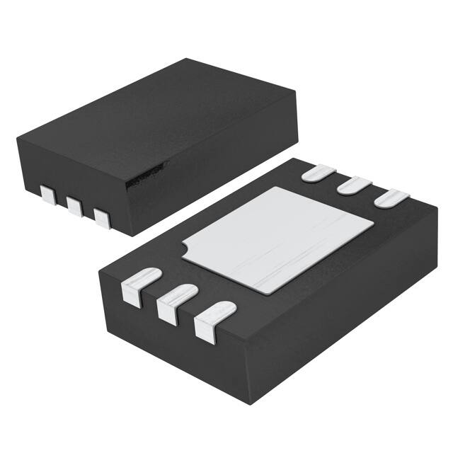
n Small 6-Pin 2mm × 3mm DFN package
n
Applications
n
n
n
n
n
Low Power Handheld Products
Cellular Phones
MP3 Players
Cameras
GPS
The LTC®2942-1 measures battery charge state, battery
voltage and chip temperature in handheld PC and portable
product applications. Its operating range is perfectly
suited for single cell Li-Ion batteries. A precision coulomb
counter integrates current through an internal sense
resistor between the battery’s positive terminal and the
load or charger. Battery voltage and on-chip temperature
are measured with an internal 14-bit No Latency ∆Σ™
ADC. The three measured quantities (charge, voltage and
temperature) are stored in internal registers accessible via
the onboard SMBus/I2C interface.
The LTC2942-1 features programmable high and low
thresholds for all three measured quantities. If a programmed threshold is exceeded, the device communicates
an alert using either the SMBus alert protocol or by setting
a flag in the internal status register.
L, LT, LTC, LTM, Linear Technology and the Linear logo are registered trademarks and
No Latency ∆Σ, ThinSOT and Bat-Track are trademarks of Linear Technology Corporation.
All other trademarks are the property of their respective owners.
Typical Application
Total Charge Error vs Sense Current
1.00
SENSE+
0.1µF
LTC2942-1
I2C/SMBus
TO HOST
AL/CC
SDA
SENSE–
SCL
GND
+
1-CELL
Li-Ion
29421 TA01a
CHARGE ERROR (%)
LOAD
CHARGER
VSENSE+ = 3.6V
0.75
0.50
0.25
0
–0.25
–0.50
–0.75
–1.00
1
10
100
|ISENSE| (mA)
1000
29421 TA01b
29421f
�
�LTC2942-1
Absolute Maximum Ratings
(Notes 1, 2)
Pin Configuration
Supply Voltage (SENSE+).............................. –0.3V to 6V
SCL, SDA, AL/CC.......................................... –0.3V to 6V
Sense Current (into SENSE–).....................................±2A
Operating Ambient Temperature Range
LTC2942-1C.............................................. 0°C to 70°C
LTC2942-1I........................................... –40°C to 85°C
Storage Temperature Range.................... –65°C to 150°C
TOP VIEW
6 SENSE–
SENSE+ 1
7
GND 2
5 AL/CC
4 SDA
SCL 3
DCB PACKAGE
6-LEAD (2mm s 3mm) PLASTIC DFN
TJMAX = 150°C, θJA = 160°C/W (Note 9)
EXPOSED PAD (PIN 7): DO NOT CONNECT
Order Information
Lead Free Finish
TAPE AND REEL (MINI)
TAPE AND REEL
PART MARKING*
PACKAGE DESCRIPTION
TEMPERATURE RANGE
LTC2942CDCB-1#TRMPBF LTC2942CDCB-1#TRPBF
LDYR
6-Lead (2mm × 3mm) Plastic DFN
0°C to 70°C
LTC2942IDCB-1#TRMPBF
LDYR
LTC2942IDCB-1#TRPBF
6-Lead (2mm × 3mm) Plastic DFN
TRM = 500 pieces. *Temperature grades are identified by a label on the shipping container.
Consult LTC Marketing for parts specified with wider operating temperature ranges.
Consult LTC Marketing for information on lead based finish parts.
For more information on lead free part marking, go to: http://www.linear.com/leadfree/
For more information on tape and reel specifications, go to: http://www.linear.com/tapeandreel/
–40°C to 85°C
Electrical
Characteristics
The l denotes the specifications which apply over the full operating
temperature range, otherwise specifications are at TA = 25°C. (Note 2)
SYMBOL
PARAMETER
CONDITIONS
MIN
TYP
MAX
UNITS
Power Requirements
VSENSE+
Supply Voltage
ISUPPLY
Supply Current (Note 3)
2.7
5.5
V
70
100
120
µA
µA
l
300
400
µA
Battery Gas Gauge On, ADC Converting Temperature l
350
450
µA
2.5
µA
Battery Gas Gauge On, ADC Sleep
l
Battery Gas Gauge On, ADC Converting Voltage
Shutdown
l
Shutdown, VSENSE+ ≤ 4.2V
VUVLO
Undervoltage Lockout Threshold
VSENSE+ Falling
l
2.5
2.6
1
µA
2.7
V
±1
A
100
mΩ
Coulomb Counter
ISENSE–
Sense Current
RSENSE
Internal Sense Resistance
RPP
Pin-to-Pin Resistance from
SENSE+ to SENSE–
(Note 8)
qLSB
Charge LSB (Note 4)
Prescaler M = 128 (Default)
Total Charge Error (Note 5)
0.2A ≤ |ISENSE–| ≤ 1A DC
TCE
l
50
50
mΩ
0.085
0.2A ≤ |ISENSE–| ≤ 1A DC, 0°C to 70°C
0.02A ≤ |ISENSE–| ≤ 1A DC (Note 8)
74
l
mAh
±1
%
±1.8
%
±2.8
%
29421f
�
�LTC2942-1
Electrical
Characteristics
The l denotes the specifications which apply over the full operating
temperature range, otherwise specifications are at TA = 25°C. (Note 2)
SYMBOL
PARAMETER
CONDITIONS
MIN
TYP
MAX
UNITS
Voltage Measurement ADC
Resolution (No Missing Codes)
VFS
Full-Scale Voltage
∆VLSB
Quantization Step of 14-Bit
Voltage ADC
TUEV
Voltage Total Unadjusted Error
(Note 8)
l
14
l
(Note 6)
Bits
6
V
366.2
µV
1
1.3
l
Gain
Gain Accuracy
VOS
Offset
INL
Integral Nonlinearity
l
tCONV
Conversion Time
l
l
Extrapolated from Measurements at 5.5V and 2.7V
±1
±1
%
%
1.3
%
±10
LSB
±4
LSB
15
ms
Temperature Measurement ADC
Resolution (No Missing Code)
(Note 8)
TFS
Full-Scale Temperature
(Note 10)
∆TLSB
Quantization Step of 10-Bit
Temperature ADC
(Note 6)
TUET
Temperature Total Unadjusted
Error
VSENSE+ ≥ 2.8V (Note 8)
tCONV
Conversion Time
10
l
Bits
600
K
0.586
K
l
±5
±3
K
K
l
15
ms
Digital Inputs and Digital Outputs
VITH
Logic Input Threshold, AL/CC,
SCL, SDA
l
VOL
Low Level Output Voltage, AL/CC, I = 3mA
SDA
l
IIN
Input Leakage, AL/CC, SCL, SDA
VIN = VSENSE+/2
CIN
Input Capacitance, AL/CC, SCL,
SDA
(Note 8)
tPCC
Minimum Charge Complete (CC)
Pulse Width
0.3 • VSENSE+
0.7 • VSENSE+
V
0.4
V
l
1
µA
l
10
pF
1
µs
I2C Timing Characteristics
fSCL(MAX)
Maximum SCL Clock Frequency
l
tBUF(MIN)
Bus Free Time Between Stop/Start
l
1.3
µs
tSU,STA(MIN) Minimum Repeated Start Set-Up
Time
l
600
ns
tHD,STA(MIN) Minimum Hold Time (Repeated)
Start Condition
l
600
ns
tSU,STO(MIN) Minimum Set-Up Time for Stop
Condition
l
600
ns
tSU,DAT(MIN) Minimum Data Setup Time Input
l
100
ns
400
900
kHz
29421f
�
�LTC2942-1
Electrical
Characteristics
The l denotes the specifications which apply over the full operating
temperature range, otherwise specifications are at TA = 25°C. (Note 2)
SYMBOL
PARAMETER
CONDITIONS
MIN
TYP
MAX
UNITS
tHD,DATI(MIN) Minimum Data Hold Time Input
l
0
µs
tHD,DATO
Data Hold Time Output
l
0.3
0.9
µs
tof
Data Output Fall Time
l
20 + 0.1 • CB
300
ns
(Notes 7, 8)
Note 1: Stresses beyond those listed under Absolute Maximum Ratings
may cause permanent damage to the device. Exposure to any Absolute
Maximum Rating condition for extended periods may affect device
reliability and lifetime.
Note 2: All currents into pins are positive, all voltages are referenced to
GND unless otherwise specified
Note 3: ISUPPLY = ISENSE+ + ISENSE–
Note 4: The equivalent charge of an LSB in the accumulated charge
register depends on the setting of the internal prescaling factor M:
qLSB = 0.085mAh •
M
128
See Choosing Coulomb Counter Prescaler M section for more information.
1mAh = 3.6C (Coulombs).
Note 5: Deviation of qLSB from its nominal value. Data is for a new device
and does not include long-term sense resistor aging. See the Internal
Sense Resistor section for more information.
Note 6: The quantization step of the 14-bit ADC in voltage mode and
10-bit ADC in temperature mode is not to be mistaken with the LSB of the
combined 16-bit voltage registers (I, J) and 16-bit temperature registers
(M, N).
Note 7: CB = Capacitance of one bus line in pF (10pF ≤ CB ≤ 400pF). See
Voltage and Temperature Registers section for more information.
Note 8: Guaranteed by design, not subject to test.
Note 9: Value decreases if exposed pad is soldered to large copper area.
See Power Dissipation section for more information.
Note 10: Use for scaling of temperature reading only. Do not use part
outside operating temperature range.
Timing Diagram
tof
SDA
tSU, DAT
tHD, DATO,
tHD, DATI
tSU, STA
tHD, STA
tBUF
tSU, STO
29421 F01
SCL
tHD, STA
START
CONDITION
REPEATED START
CONDITION
STOP
CONDITION
START
CONDITION
Figure 1. Definition of Timing on I2C Bus
29421f
�
�LTC2942-1
Typical Performance Characteristics
Total Charge Error
vs Sense Current
Total Charge Error
vs Supply Voltage
1.00
–0.25
–0.50
CHARGE ERROR (%)
0
0.4
0.2
0
–0.2
–0.4
–0.6
–0.75
VSENSE+ = 2.7V
VSENSE+ = 4.2V
1
10
100
|ISENSE| (mA)
–1.0
1000
2.5
3
3.5
4.5
4
VSENSE+ (V)
5
29421 G01
60
3.5
4.0 4.5
5.0
VSENSE + (V)
5.5
1.0
0
6.0
TA = 25°C
TA = –40°C
TA = 85°C
2.5
3.0
3.5
4.0 4.5
5.0
VSENSE + (V)
5.5
29421 G04
TA = 25°C
–0.5
–1.0
2.5
3.0
3.5
4.0 4.5 5.0
VSENSE – (V)
5.5
6.0
29421 G07
INL (VLSB)
100
6
TA = 85°C
4
2
0
TA = –45°C
–2
–4
–6
TA = 25°C
–8
–10
6.0
2.5
3.0
3.5
4.0 4.5
5.0
VSENSE – (V)
29421 G06
Sense Resistor Stability
3
0
2
–0.5
1
–1.0
0
ACCELERATED LOAD LIFE TEST
DATA SCALED TO TAMB = 85°C,
ISENSE = 1A CONDITIONS
–1.5
–1
–2.0
–2
–2.5
–3
–50
6.0
5.5
∆R/RO (%)
TEMPERATURE ERROR (°C)
TA = 85°C
TA = –40°C
75
24921 G03
Temperature Error vs Temperature
1.0
0
0
50
25
TEMPERATURE (°C)
29421 G05
Voltage Measurement ADC
Integral Nonlinearity
0.5
–25
8
50
3.0
|ISENSE| = 200mA
10
0.5
40
2.5
–1.00
–50
2.0
ISHUTDOWN (µA)
ISUPPLY (µA)
70
–0.50
Voltage Measurement ADC
Total Unadjusted Error
1.5
80
–0.25
Shutdown Supply Current
vs Supply Voltage
TA = 25°C
TA = –40°C
TA = 85°C
90
0
29421 G02
Supply Current vs Supply Voltage
100
6
5.5
0.25
–0.75
|ISENSE| = 1A
|ISENSE| = 200mA
–0.8
0.50
TOTAL UNADJUSTED ERROR (mV)
0.25
TEMPERATURE
COMPENSATION
TRIM DEVIATION
+50ppm/K
OPTIMUM
–50ppm/K
0.75
0.6
0.50
CHARGE ERROR (%)
CHARGE ERROR (%)
1.00
0.8
0.75
–1.00
Total Charge Error vs Temperature
1.0
–25
0
25
50
TEMPERATURE (°C)
75
100
29421 G08
–3.0
0
10
20
30
kHOURS
40
50
29421 G09
29421f
�
�LTC2942-1
Pin Functions
SENSE+ (Pin 1): Positive Current Sense Input and Power
Supply. Connect to the load and battery charger output.
VSENSE+ operating range is 2.7V to 5.5V.
GND (Pin 2): Device Ground. Connect directly to the negative battery terminal.
SCL (Pin 3): Serial Bus Clock Input.
SDA (Pin 4): Serial Bus Data Input and Output.
AL/CC (Pin 5): Alert Output or Charge Complete Input.
Configured either as an SMBus alert output or charge
complete input by control register bits B[2:1]. At power-up,
the pin defaults to alert mode conforming to the SMBus
alert response protocol. It behaves as an open-drain logic
output that pulls to GND when any threshold register value
is exceeded. When configured as a charge complete input,
a high level at CC sets the value of the accumulated charge
(registers C, D) to FFFFh. Columb counting starts when
the input returns to low level.
SENSE– (Pin 6): Negative Current Sense Input. Connect
SENSE– to the positive battery terminal. Current from/into
this pin must not exceed 1A in normal operation.
Exposed Pad (Pin 7): Do Not Connect. Soldering the
exposed pad to adequate electrically isolated copper area
is recommended for best thermal performance, and best
accuracy of the integrated temperature sensor.
Block Diagram
1
VSUPPLY
RBOND
SENSE+ 12mΩ
COULOMB COUNTER
REF
RSENSE
50mΩ
6
2
RBOND
SENSE– 12mΩ
TEMPERATURE
SENSOR
MUX
CC
CLK
REFERENCE
GENERATOR
OSCILLATOR
REF+
CLK
IN
ACCUMULATED
CHARGE
REGISTER
AL
I2C/
SMBus
AL/CC
SCL
SDA
ADC
5
3
4
DATA AND
CONTROL
REGISTERS
REF–
GND
29421 BD
Operation
Overview
The LTC2942-1 is a battery gas gauge device designed
for use with single Li-Ion cells and other battery types
with terminal voltages from 2.7V to 5.5V. It measures
battery charge and discharge, battery voltage and chip
temperature. A precision coulomb counter integrates
current through an internal sense resistor between the
�
battery’s positive terminal and the load or charger. Battery
voltage and on-chip temperature are measured with an
internal 14-bit/10-bit ADC. The integrated, temperaturecompensated sense resistor offers board space savings
and superior charge measurement accuracy in applications
with currents up to 1A.
29421f
�LTC2942-1
Operation
Coulomb Counter
Charge is the time integral of current. The LTC2942-1 measures battery current by monitoring the voltage developed
across its internal sense resistor and then integrates this
information to infer charge. The internal sense resistor is
tied between the SENSE+ and SENSE– pins and is connected to an auto-zeroed differential analog integrator
which converts the measured current to charge.
When the integrator output reaches the REFHI or REFLO
thresholds, switches S1, S2, S3 and S4 toggle to reverse
the ramp direction. By observing the condition of the
switches and the ramp direction, polarity is determined. A
programmable prescaler effectively increases integration
time by a factor M programmable from 1 to 128. At each
underflow or overflow of the prescaler, the accumulated
charge register (ACR) value is incremented or decremented
one count. The value of accumulated charge is read via
the I2C interface.
Voltage and Temperature ADC
The LTC2942-1 includes a 14-bit No Latency ∆Σ analogto-digital converter, with internal clock and voltage reference circuits.
CHARGER
LOAD
1
SENSE+
6
S1
RBOND
IBAT
BATTERY
+
2
SENSE–
RBOND
GND
Conversion of either temperature or voltage is triggered
by setting the control register via the I2C interface. The
LTC2942-1 features an automatic mode where a voltage
and a temperature conversion are executed every two
seconds. At the end of each conversion the corresponding
registers are updated and the converter goes to sleep to
minimize quiescent current.
Power-Up Sequence
When VSENSE+ rises above a threshold of approximately
2.5V, the LTC2942-1 generates an internal power-on reset
(POR) signal and sets all registers to their default state.
In the default state, the coulomb counter is active while
the voltage and temperature ADC is switched off. The
accumulated charge register is set to mid-scale (7FFFh),
all low threshold registers are set to 0000h and all high
threshold registers are set to FFFFh. The alert mode is
enabled and the coulomb counter pre-scaling factor M
is set to 128.
REFHI
VCC
RSENSE
The ADC can either be used to monitor the battery voltage
at SENSE– or to convert the output of the on-chip temperature sensor. The sensor generates a voltage proportional to
temperature with a slope of 2.5mV/K resulting in a voltage
of 750mV at 27°C.
–
+
–
CONTROL
LOGIC
S2
S3
M
PRESCALER
+
ACR
+
S4
REFLO
–
POLARITY
DETECTION
29421 F02
Figure 2. Coulomb Counter Section of the LTC2942-1
29421f
�
�LTC2942-1
Applications Information
I2C/SMBus Interface
Status Register (A)
The LTC2942-1 communicates with a bus master using a
2-wire interface compatible with I2C and SMBus. The 7-bit
hard-coded I2C address of the LTC2942-1 is 1100100.
The status of the charge, voltage and temperature alerts
is reported in the status register shown in Table 2.
The LTC2942-1 is a slave-only device. Therefore the serial
clock line (SCL) is an input only while the serial data line
(SDA) is bidirectional. The device supports I2C standard
and fast mode. For more details refer to the I2C Protocol
section.
Internal Registers
The LTC2942-1 integrates current through a sense resistor,
measures battery voltage and temperature and stores the
results in internal 16-bit registers accessible via I2C. High
and low limits can be programmed for each measurement
quantity. The LTC2942-1 continuously monitors these
limits and sets a corresponding flag in its status register
when a limit is exceeded. If the alert mode is enabled, the
AL/CC pin pulls low.
The sixteen internal registers are organized as shown in
Table 1.
Table 1. Register Map
ADDRESS NAME REGISTER DESCRIPTION
00h
A
Status
01h
B
Control
02h
C
Accumulated Charge MSB
03h
D
Accumulated Charge LSB
04h
E
Charge Threshold High MSB
05h
F
Charge Threshold High LSB
06h
G
Charge Threshold Low MSB
07h
H
Charge Threshold Low LSB
08h
I
Voltage MSB
09h
J
Voltage LSB
0Ah
K
Voltage Threshold High
0Bh
L
Voltage Threshold Low
0Ch
M
Temperature MSB
0Dh
N
Temperature LSB
0Eh
O
Temperature Threshold High
0Fh
P
Temperature Threshold Low
R = Read, W = Write, XX = unknown
R/W DEFAULT
R See Below
R/W
3Ch
R/W
7Fh
R/W
FFh
R/W
FFh
R/W
FFh
R/W
00h
R/W
00h
R
XXh
R
XXh
R/W
FFh
R/W
00h
R
XXh
R
XXh
R/W
FFh
R/W
00h
Table 2. Status Register A (Read only)
BIT
NAME
OPERATION
DEFAULT
A[7] Chip Identification
0: LTC2942-1
1: LTC2941-1
0
A[6] Reserved
Not Used.
0
A[5] Accumulated Charge Indicates that the value of the
Overflow/Underflow accumulated charge hit either
top or bottom.
0
A[4] Temperature Alert
Indicates one of the
temperature limits was
exceeded.
0
A[3] Charge Alert High
Indicates that the accumulated
charge value exceeded the
charge threshold high limit.
0
A[2] Charge Alert Low
Indicates that the accumulated
charge value dropped below
the charge threshold low limit.
0
A[1] Voltage Alert
Indicates one of the battery
voltage limits was exceeded.
0
A[0] Undervoltage
Lockout Alert
Indicates recovery from
undervoltage. If set to 1, a
UVLO has occurred and the
content of the registers is
uncertain.
X
All status register bits except A[7] are cleared after being
read by the host, if the conditions which set these bits
have been removed.
As soon as one of the three measured quantities exceeds
the programmed limits, the corresponding bit A[4], A[3],
A[2] or A[1] in the status register is set.
Bit A[5] is set if the LTC2942-1’s accumulated charge
registers (ACR) overflows or underflows. In these cases,
the ACR stays at FFFFh or 0000h and does not roll over.
The undervoltage lockout (UVLO) bit of the status register
A[0] is set if, during operation, the voltage on SENSE+
pin drops below 2.7V without reaching the POR level.
The analog parts of the coulomb counter are switched off
while the digital register values are retained. After recovery of the supply voltage the coulomb counter resumes
integrating with the stored value in the accumulated
charge registers but it has missed any charge flowing
while SENSE+ < 2.7V.
29421f
�
�LTC2942-1
Applications Information
The hard-coded bit A[7] of the status register enables the
host to distinguish the LTC2942-1 from the pin compatible LTC2941, allowing the same software to be used with
both devices.
Control Register (B)
The operation of the LTC2942-1 is controlled by programming the control register. Table 3 shows the organization
of the 8-bit control register B[7:0].
Table 3. Control Register B
BIT
NAME
B[7:6] ADC Mode
B[5:3] Prescaler M
OPERATION
[00]
Sets coulomb counter prescaling
factor M between 1 and 128.
Default is 128.
M = 2(4 • B[5] + 2 • B[4] + B[3])
[111]
B[2:1] AL/CC Configure Configures the AL/CC pin.
[10] Alert Mode.
Alert functionality enabled.
Pin becomes logic output.
[01] Charge Complete Mode.
Pin becomes logic input and
accepts “charge complete” signal
(e.g., from a charger) to set
accumulated charge register (C,D)
to FFFFh.
[00] AL/CC pin disabled.
[11] Not allowed.
B[0]
Shutdown
Default
[11] Automatic Mode.
Performs voltage and temperature
conversion every second.
[10] Manual Voltage Mode.
Performs single voltage
conversion, then sleeps.
[01] Manual Temperature Mode.
Performs single temperature
conversion, then sleeps.
[00] Sleep.
Shut down analog section to
reduce ISUPPLY.
Alert/Charge Complete Configuration B[2:1]
The AL/CC pin is a dual function pin configured by the
control register. By setting bits B[2:1] to [10] (default)
the AL/CC pin is configured as an alert pin following the
SMBus protocol. In this configuration the AL/CC pin is a
digital output and is pulled low if one of the three measured quantities (charge, voltage, temperature) exceeds
its high or low threshold or if the value of the accumulated
charge register overflows or underflows. An alert response
procedure started by the master resets the alert at the
AL/CC pin. For further information see the Alert Response
Protocol section.
Setting the control bits B[2:1] to [01] configures the AL/CC
pin as a digital input. In this mode, a high input on the
AL/CC pin communicates to the LTC2942-1 that the battery is full and the accumulated charge register is set to
its maximum value FFFFh. Columb counting starts when
the AL/CC pin returns to low level.
[10]
If neither the alert nor the charge complete functionality
is desired, bits B[2:1] should be set to [00]. The AL/CC
pin is then disabled and should be tied to GND.
Avoid setting B[2:1] to [11] as it enables the alert and the
charge complete modes simultaneously.
Choosing Coulomb Counter Prescaler ‘M’ B[5:3]
To use as much of the range of the accumulated charge
register as possible the prescaler factor M is chosen based
on battery capacity QBAT :
[0]
Power Down B[0]
Programming the last bit B[0] of the control register to 1
sets the analog parts of the LTC2942-1 in power down and
the current consumption drops typically below 1µA. All
analog circuits are disabled while the values in the registers
are retained. Note that any charge flowing while B[0] is 1
is not measured and the charge information below 1LSB
of the accumulated charge register is lost.
M ≥ 128 •
16
2
QBAT
• 0.085mAh
=
23
•Q
Ah BAT
M can be set to 1, 2, 4, 8,... 128 by programming B[5:3] of
the control register as M = 2(4 • B[5] + 2 • B[4] + B[3]). The default
value after power up is M = 128 = 27 (B[5:3] = 111). The
maximum battery capacity supported within the prescaler
range is 5.5Ah with M = 128. See the section Extending
Coulomb Counter Range if battery capacity is higher.
Depending on the choice of prescaler factor M, the charge
LSB of the accumulated charge register becomes:
qLSB = 0.085mAh •
M
128
29421f
�
�LTC2942-1
Applications Information
Note that the internal digital resolution of the coulomb
counter is higher than indicated by qLSB. The internal
charge resolution is typically 299µAs.
a given register contents (C[7:0]D[7:0]) and prescaler
setting M can be calculated by:
ADC Mode B[7:6]
The LTC2942-1 features an ADC which measures either
voltage on SENSE– (battery voltage) or temperature via
an internal temperature sensor. The reference voltage and
clock for the ADC are generated internally.
The ACR should be read in a single I2C Read transaction
(see Figure 10). If C and D are read in individual singlebyte transactions, each with a STOP condition, the register
may change between the first and the second transaction
due to coulomb count events, causing erroneous charge
readings.
The ADC has four different modes of operation as shown
in Table 3. These modes are controlled by bits B[7:6] of
the control register. At power-up, bits B[7:6] are set to
[00] and the ADC is in sleep mode.
A single voltage conversion is initiated by setting the bits
B[7:6] to [10]. A single temperature conversion is started
by setting bits B[7:6] to [01]. After a single voltage or
temperature conversion, the ADC resets B[7:6] to [00]
and goes to sleep.
The LTC2942-1 also offers an automatic scan mode where
the ADC converts voltage, then temperature, then sleeps
for approximately two seconds before repeating the voltage
and temperature conversions. The LTC2942-1 is set to this
automatic mode by setting B[7:6] to [11] and stays in this
mode until B[7:6] are reprogrammed by the host.
Programming B[7:6] to [00] puts the ADC to sleep. If
control bits B[7:6] change within a conversion, the ADC
will complete the current conversion before entering the
newly selected mode.
A conversion of either voltage or temperature requires 10ms
conversion time (typical). At the end of each conversion,
the corresponding registers are updated. If the converted
quantity exceeds the values programmed in the threshold
registers, a flag is set in the status register and the AL/CC
pin is pulled low (if alert mode is enabled).
Accumulated Charge Register (C,D)
The coulomb counter of the LTC2942-1 integrates current
through its internal sense resistor over time. The result of
this charge integration is stored in the 16-bit accumulated
charge register (registers C, D). The amount of charge for
Q = 0.085mAh •
M
• (C • 256 + D)
128
As the LTC2942-1 does not know the actual battery status
at power-up, the accumulated charge register (ACR) is set
to mid-scale (7FFFh). If the host knows the status of the
battery, the accumulated charge (C[7:0]D[7:0]) can be
either programmed to the correct value via I2C or it can be
set after charging to FFFFh (full) by pulling the AL/CC pin
high if charge complete mode is enabled via bits B[2:1]. In
this case, FFFFh represents a fully charged battery. If the
actual battery capacity is smaller, the host can subtract the
excess charge whenever doing the charge calculation, and
set the low charge threshold (registers G,H) to the value
representing an empty battery. This procedure essentially
shifts the zero point of the scale upwards. Before writing
the accumulated charge registers, the analog section
should be shut down by setting B[0] to 1.
Voltage and Temperature Registers (I, J),(M, N)
The result of the 14-bit ADC conversion of the voltage at
SENSE– is stored in the voltage registers (I, J), whereas
the temperature measurement result is stored in the temperature registers (M, N). The voltage and temperature
registers are read only.
As the ADC resolution is 14-bit in voltage mode and 10-bit
in temperature mode, the lowest two bits of the combined
voltage registers (I, J) and the lowest six bits of the
combined temperature registers (M, N) are always zero.
From the result of the 16-bit voltage registers I[7:0]J[7:0]
the measured voltage can be calculated as:
VSENSE– = 6 V •
RESULTDEC
RESULTh
= 6V •
FFFFh
65535
29421f
10
�LTC2942-1
Applications Information
Example: a register value of I[7:0] = B0h and J[7:0] = 1Ch
corresponds to a voltage on SENSE– of:
VSENSE– = 6 V •
45084DEC
B01Ch
= 6V •
≈ 4.1276 V
FFFFh
65535
Voltage is measured at the internal bond pads connected to
SENSE–, hence, the current flowing through the combined
pin and bond wire resistance causes the measured voltage
to deviate slightly from the actual battery voltage at the
SENSE– package pin. For the full-scale current of ±1A at
room temperature, this error is typically ±9mV, which is
negligible in most applications. To increase the precision
of the voltage measurement, the error can be reduced by
differentiating the coulomb counter data, multiplying the
resultant current value by 9 mΩ, and adding or subtracting the result from the voltage measurement. Note that
the sign of the error changes depending on the direction
of the current flow.
The actual temperature can be obtained from the two byte
register C[7:0]D[7:0] by:
T = 600K •
RESULTDEC
RESULTh
= 600K •
FFFFh
65535
Example: a register value of C[7:0] = 80h D[7:0] = 00h
corresponds to 300K or 27°C.
Temperature is measured on the surface of the chip (TDIE),
which may be different from ambient temperature TAMB,
especially with high sense resistor currents. To minimize
errors in the temperature measurement, the DFN package’s
exposed pad may be thermally coupled to the body whose
temperature is to be measured. With the recommended PCB
layout (Figure 11), TDIE typically increases over TAMB by
1K for 0.25A, 3K for 0.5A and 12K for 1A. Different results
may be obtained depending on layout, mounting details,
and air flow. Software in the host system can reduce this
error if the rise over TAMB is known by differentiating the
coulomb counter data to obtain current and using this
value to correct the temperature reading.
Threshold Registers (E, F, G, H, K, L, O, P)
For each of the measured quantities (battery charge, voltage and temperature) the LTC2942-1 features a high and a
low threshold registers. At power-up, the high thresholds
are set to FFFFh while the low thresholds are set to 0000h.
All thresholds can be programmed to a desired value via
I2C. As soon as a measured quantity exceeds the high
threshold or falls below the low threshold, the LTC2942‑1
sets the corresponding flag in the status register and
pulls the AL/CC pin low if alert mode is enabled via bits
B[2:1]. Note that the voltage and temperature threshold
registers are single byte registers and only the 8 MSBs of
the corresponding quantity are checked. To set a low level
threshold for the battery voltage of 3V, register L should
be programmed to 80h; a high temperature limit of 60°C
is programmed by setting register O to 8Eh.
I2C Protocol
The LTC2942-1 uses an I2C/SMBus compatible 2-wire
open-drain interface supporting multiple devices and
masters on a single bus. The connected devices can only
pull the bus wires low and they never drive the bus high.
The bus wires must be externally connected to a positive
supply voltage via a current source or pull-up resistor.
When the bus is idle, both SDA and SCL are high. Data on
the I2C bus can be transferred at rates of up to 100kbit/s
in standard mode and up to 400kbit/s in fast mode.
Each device on the I2C/SMbus is recognized by a unique
address stored in that device and can operate as either a
transmitter or receiver, depending on the function of the
device. In addition to transmitters and receivers, devices
can also be classified as masters or slaves when performing data transfers. A master is the device which initiates a
data transfer on the bus and generates the clock signals
to permit that transfer. At the same time any device addressed is considered a slave. The LTC2942-1 always
acts as a slave.
Figure 3 shows an overview of the data transmission for
fast and standard mode on the I2C bus.
Start and Stop Conditions
When the bus is idle, both SCL and SDA must be high. A
bus master signals the beginning of a transmission with
a START condition by transitioning SDA from high to low
while SCL is high. When the master has finished communicating with the slave, it issues a STOP condition by
29421f
11
�LTC2942-1
Applications Information
transitioning SDA from low to high while SCL is high. The
bus is then free for another transmission. When the bus is
in use, it stays busy if a repeated START (Sr) is generated
instead of a STOP condition. The repeated START (Sr)
conditions are functionally identical to the START (S).
Data Transmission
After a START condition, the I2C bus is considered busy
and data transfer begins between a master and a slave. As
data is transferred over I2C in groups of nine bits (eight
data bits followed by an acknowledge bit), each group
takes nine SCL cycles. The transmitter releases the SDA
line during the acknowledge clock pulse and the receiver
issues an acknowledge (ACK) by pulling SDA low or leaves
SDA high to indicate a not acknowledge (NAK) condition.
Change of data state can only happen while SCL is low.
Write Protocol
The master begins a write operation with a START condition followed by the seven bit slave address 1100100
and the R/W bit set to zero, as shown in Figure 4. The
LTC2942-1 acknowledges this by pulling SDA low and then
the master sends a command byte which indicates which
internal register the master is to write. The LTC2942‑1
acknowledges and latches the command byte into its
internal register address pointer. The master delivers the
data byte, the LTC2942-1 acknowledges once more and
latches the data into the desired register. The transmission
is ended when the master sends a STOP condition. If the
master continues by sending a second data byte instead
of a stop, the LTC2942-1 acknowledges again, increments
its address pointer and latches the second data byte in the
following register, as shown in Figure 5.
Read Protocol
The master begins a read operation with a START condition
followed by the seven bit slave address 1100100 and the
R/W bit set to zero, as shown in Figure 6. The LTC2942-1
acknowledges and then the master sends a command byte
which indicates which internal register the master is to
read. The LTC2942-1 acknowledges and then latches the
command byte into its internal register address pointer. The
master then sends a repeated START condition followed
by the same seven bit address with the R/W bit now set
12
to one. The LTC2942-1 acknowledges and sends the contents of the requested register. The transmission is ended
when the master sends a STOP condition. If the master
acknowledges the transmitted data byte, the LTC2942-1
increments its address pointer and sends the contents of
the following register as depicted in Figure 7.
Alert Response Protocol
In a system where several slaves share a common interrupt line, the master can use the alert response address
(ARA) to determine which device initiated the interrupt
(Figure 8).
The master initiates the ARA procedure with a START condition and the special 7-bit ARA bus address (0001100)
followed by the read bit (R) = 1. If the LTC2942-1 is asserting the AL/CC pin in alert mode, it acknowledges and
responds by sending its 7-bit bus address (1100100) and
a 1. While it is sending its address, it monitors the SDA pin
to see if another device is sending an address at the same
time using standard I2C bus arbitration. If the LTC2942-1
is sending a 1 and reads a 0 on the SDA pin on the rising
edge of SCL, it assumes another device with a lower address is sending and the LTC2942-1 immediately aborts
its transfer and waits for the next ARA cycle to try again.
If transfer is successfully completed, the LTC2942-1 will
stop pulling down the AL/CC pin and will not respond to
further ARA requests until a new Alert event occurs.
Internal Sense Resistor
The internal sense resistor uses proprietary* temperature compensation techniques to reduce the effective
temperature coefficient to less than ±50 ppm/K typically.
The effective sense resistance as seen by the coulomb
counter is factory trimmed to 50mΩ. Both measures,
and the lack of thermocouple effects in the sense resistor connections, contribute to the LTC2942-1’s superior
charge measurement accuracy compared to competing
solutions employing a common 1% tolerance, 50ppm/K
tempco discrete current sense resistor.
Like all sense resistors, the integrated sense resistor in
the LTC2942-1 will exhibit minor long-term resistance
shift. The resistance typically drops less than –0.1% per
*Patent pending.
29421f
�LTC2942-1
Applications Information
1000h at 1A current and 85°C ambient temperature; this
outperforms most types of discrete sense resistors except
those of the very high and ultrahigh stability variety. See
the Typical Performance Characteristics for expected
resistor drift performance under worst-case conditions.
Drift will be much slower at lower temperatures. Contact
LTC applications for more information.
sense resistor drift over product lifetime or calibration
intervals is less than –2%.
For most coulomb counter applications this aging behavior
of the integrated sense resistor is insignificant compared
to the change of battery capacity due to battery aging.
The LTC2942-1 is factory trimmed to optimum accuracy
when new; for applications which require the best possible
coulomb count accuracy over the full product lifetime, the
coulomb counter gain can be adjusted in software. For
instance, if the error contribution of sense resistor drift
must be limited to ±1%, coulomb counts may be biased
high by 1% (use factor 1.01), and maximum operational
temperature and current then must be derated such that
Voltage Drop Between SENSE+ and SENSE–
SDA
a6 - a0
SCL
1-7
8
9
ADDRESS
R/W
ACK
Applications employing the standard external resistor
LTC2942 with an external 50mΩ sense resistor may be
upgraded to the pin-compatible LTC2942-1 by removing
the external sense resistor.
The LTC2942-1 is trimmed for an effective internal resistance of 50mΩ , but the total pin-to-pin resistance (RPP),
consisting of the sense resistor in series with pin and bond
wire resistances, is somewhat higher. Assuming a sense
resistor temperature coefficient of about 3900ppm/K,
the total resistance between SENSE+ and SENSE– at a
temperature T is typically:
RPP(T) = RPP(TNOM) [1 + 0.0039(T – TNOM)]
b7 - b0
b7 - b0
1-7
8
9
1-7
8
9
S
P
START
CONDITION
DATA
ACK
DATA
ACK
Figure 3. Data Transfer Over I2C or SMBus
S
ADDRESS
W
A
REGISTER
A
DATA
A
1100100
0
0
01h
0
FCh
0
STOP
CONDITION
29421 F03
P
29421 F04
FROM MASTER TO SLAVE
A: ACKNOWLEDGE (LOW)
A: NOT ACKNOWLEDGE (HIGH)
FROM SLAVE TO MASTER
S: START CONDITION
P: STOP CONDITION
R: READ BIT (HIGH)
W: WRITE BIT (LOW)
Figure 4. Writing FCh to the LTC2942-1 Control Register (B)
S
ADDRESS
W
A
REGISTER
A
DATA
A
DATA
A
1100100
0
0
02h
0
F0h
0
01h
0
P
S
ADDRESS
W
A
REGISTER
A
1100100
0
0
00h
0
S
ADDRESS
R
A
DATA
A
1100100
1
0
01h
1
29421 F05
29421 F06
Figure 5. Writing F001h to the LTC2942-1
Accumulated Charge Register (C, D)
S
P
Figure 6. Reading the LTC2942-1 Status Register (A)
ADDRESS
W
A
REGISTER
A
1100100
0
0
08h
0
S
ADDRESS
R
A
DATA
A
DATA
A
1100100
1
0
F1h
0
24h
1
P
29421 F07
Figure 7. Reading the LTC2942-1 Voltage Register (I, J)
29421f
13
�LTC2942-1
Applications Information
S
ALERT RESPONSE ADDRESS
R
A
DEVICE ADDRESS
A
0001100
1
0
11001001
1
P
29421 F08
Figure 8. LTC2942-1 Serial Bus SDA Alert Response Protocol
S ADDRESS W A REGISTER A DATA P
1100100 0 0
01h
0
S ADDRESS W A REGISTER A S ADDRESS R A DATA A DATA A P
10ms
1100100 0 0
BC
08h
0
1100100 1 0 F1h 0 80h 1
29421 F09
Figure 9. Voltage Conversion Sequence
S
ADDRESS
W
A
REGISTER
A
1100100
0
0
02h
0
S
ADDRESS
R
A
DATA
A
DATA
A
1100100
1
0
80h
0
01h
1
P
29421 F10
Figure 10. Reading the LTC2942-1 Accumulated Charge Registers (C, D)
where TNOM = 27°C (or 300K) and RPP(TNOM) is from
the Electrical Characteristics table. This means that the
resistance between SENSE+ and SENSE– may drop by
26% if die temperature changes from 27°C to –40°C
or increase by 23% for a 27°C to 85°C die temperature
change. Ensure that total voltage drop between SENSE+
and SENSE–, caused by maximum peak current flowing
in/out of SENSE–:
Power Dissipation
VDROP = IPEAK • RPP(TDIE(MAX))
TDIE = TAMB + 1.22 • θJA • RPP(MAX) • ISENSE2
does not exceed the application’s requirements.
Limiting Inrush Current
Inrush currents during events like battery insertion or
closure of a mechanical power switch may be substantially higher than peak currents during normal operation.
Extremely large inrush currents may require additional
circuitry to keep currents through the LTC2942-1 sense
resistor below the absolute maximum ratings.
Note that external Schottky clamp diodes between SENSE+
and SENSE– can leak significantly, especially at high temperature, which can cause significant coulomb counter
errors. Preferred solutions to limit inrush current include
active Hot Swap™ current limiting or connector designs
that include current limiting resistance and staggered pins
to ensure a low impedance connection when the connector
is fully mated.
Power dissipation in the RPP resistance when operated
at high currents can increase the die temperature several degrees over ambient. Soldering the exposed pad
of the DFN package to a large copper region on the PCB
is recommended for applications operating close to the
specified maximum current and ambient temperature. Die
temperature at a given ISENSE can be estimated by:
where the factor 1.22 approximates the effect of sense
resistor self-heating, RPP(MAX) is the maximum pad-topad resistance at nominal temperature (27°C) and θJA is
the thermal resistance from junction to ambient. The θJA
data given for the DFN package is valid for typical PCB
layouts; more precise θJA data for a particular PCB layout
may be obtained by measuring the voltage VP-P between
SENSE+ and SENSE–, the ambient temperature TAMB, and
the die temperature TDIE, and calculating:
θ JA =
TDIE – TAMB
VP-P • ISENSE
Both TAMB and TDIE temperature may be measured using
the internal temperature sensor included in the LTC2942-1.
ISENSE should be set to zero to measure TAMB, and high
enough during TDIE measurement to achieve a significant
temperature increase over TAMB.
29421f
14
�LTC2942-1
Applications Information
Measuring Current
In some applications, it may be desirable to measure the
current ISENSE flowing through the internal sense resistor.
Since charge measured by the coulomb counter is the
time integral over ISENSE, differentiation of the contents
of the accumulated charge register (ACR) over time may
be used to measure average current.
Accuracy of such an indirect current measurement is limited
by the basic accuracy of the coulomb counter, the accuracy
of the timebase within the host system, quantization caused
by the prescaler setting, and time delays caused by I2C
transactions. Still, especially at higher currents, useful
results may be obtained by reading the accumulated charge
register twice, with a defined time interval in between, and
dividing the charge difference by the time interval. The
time interval may be increased at low currents to limit time
quantization errors to the desired accuracy. For quicker
current measurements at low currents, prescale factor M
may be temporarily decreased, sacrificing some coulomb
count accuracy for higher current resolution.
the threshold registers to determine when the accumulated
charge register approaches the minimum or maximum
limits. At this point it can add or subtract a fixed charge
quantity and rewrite the result into the ACR. The added
or subtracted charge quantities can then be tracked in
software, increasing the effective ACR range.
PC Board Layout Suggestions
Keep all traces as short as possible to minimize noise and
inaccuracy. Use wider traces from the resistor to the battery, load and/or charger (see Figure 11). Put the bypass
capacitor close to SENSE+ and GND. Provide adequate
copper area on exposed pad for heat sinking.
ELECTRICALLY ISOLATED HEAT SINK
TO
CHARGER/LOAD
2
5
4
CONNECTED TO EXPOSED PAD ONLY
To increase the range of the coulomb counter for battery
capacities higher than 5.5Ah, the host controller can either
regularly poll the accumulated charge register (ACR) or use
Package Description
LTC2942-1
3
Extending Coulomb Counter Range
TO BATTERY
6
1
C
29421 F11
Figure 11. Recommended Layout
DCB Package
6-Lead Plastic DFN (2mm × 3mm)
(Reference LTC DWG # 05-08-1715)
R = 0.115
TYP
2.00 p0.10
(2 SIDES)
R = 0.05
TYP
0.70 p0.05
3.55 p0.05
3.00 p0.10
(2 SIDES)
1.65 p0.05
(2 SIDES)
0.40 p 0.10
4
6
1.65 p 0.10
(2 SIDES)
2.15 p0.05
PACKAGE
OUTLINE
PIN 1 NOTCH
R0.20 OR 0.25
s 45o CHAMFER
PIN 1 BAR
TOP MARK
(SEE NOTE 6)
3
0.25 p 0.05
0.50 BSC
1.35 p0.05
(2 SIDES)
0.200 REF
RECOMMENDED SOLDER PAD PITCH AND DIMENSIONS
NOTE:
1. DRAWING TO BE MADE A JEDEC PACKAGE OUTLINE M0-229 VARIATION OF (TBD)
2. DRAWING NOT TO SCALE
3. ALL DIMENSIONS ARE IN MILLIMETERS
0.75 p0.05
1
(DCB6) DFN 0405
0.25 p 0.05
0.50 BSC
1.35 p0.10
(2 SIDES)
0.00 – 0.05
BOTTOM VIEW—EXPOSED PAD
4. DIMENSIONS OF EXPOSED PAD ON BOTTOM OF PACKAGE DO NOT INCLUDE
MOLD FLASH. MOLD FLASH, IF PRESENT, SHALL NOT EXCEED 0.15mm ON ANY SIDE
5. EXPOSED PAD SHALL BE SOLDER PLATED
6. SHADED AREA IS ONLY A REFERENCE FOR PIN 1 LOCATION ON THE
TOP AND BOTTOM OF PACKAGE
29421f
Information furnished by Linear Technology Corporation is believed to be accurate and reliable.
However, no responsibility is assumed for its use. Linear Technology Corporation makes no representation that the interconnection of its circuits as described herein will not infringe on existing patent rights.
15
�LTC2942-1
Typical Application
Single Cell Lithium-Ion Coulomb Counter with Battery Charger for Discharge Currents of up to 1A
4
VIN
5V
VCC
BAT
3
3.3V
LTC4057-4.2
(CHARGER)
1µF
5
2k
PROG SHDN
GND
LOAD
0.1µF
2k
1
VDD
µP
2
2k
2k
1
SENSE+
LTC2942-1
5
AL/CC
4
6
SDA
SENSE–
3
+
SCL
GND
1-CELL
Li-Ion
2
29421 TA02
Related Parts
PART NUMBER
DESCRIPTION
COMMENTS
Battery Gas Gauges
LTC2942
Battery Gas Gauge with I2C Interface and Voltage and
Temperature ADC
2.7V to 5.5V Operation, 14-Bit ∆∑-ADC, Pin Compatible with LTC2941
LTC2941
Battery Gas Gauge with I2C Interface
2.7V to 5.5V Operation, Pin Compatible with LTC2942
LTC2941-1
Battery Gas Gauge with I2C Interface and Integrated
2.7V to 5.5V Operation, Pin Compatible with LTC2942-1
LTC4150
Coulomb Counter/Battery Gas Gauge
2.7V to 8.5V Operation, 10-Pin MSOP Package
LTC1734
Lithium-Ion Battery Charger in ThinSOT™
Simple ThinSOT Charger, No Blocking Diode, No Sense Resistor Needed
LTC4002
Switch Mode Lithium-Ion Battery Charger
Standalone, 4.7V ≤ VIN ≤ 24V, 500kHz Frequency
LTC4052
Monolithic Lithium-Ion Battery Pulse Charger
No Blocking Diode or External Power FET Required, ≤1.5A Charge Current
LTC4053
USB Compatible Monolithic Li-Ion Battery Charger
Standalone Charger with Programmable Timer, Up to 1.25A Charge Current
LTC4057
Lithium-Ion Linear Battery Charger
Up to 800mA Charge Current, Thermal Regulation, ThinSOT Package
LTC4058
Standalone 950mA Lithium-Ion Charger in DFN
C/10 Charge Termination, Battery Kelvin Sensing, ±7% Charge Accuracy
LTC4059
900mA Linear Lithium-Ion Battery Charger
2mm × 2mm DFN Package, Thermal Regulation, Charge Current Monitor
Output
LTC4061
Standalone Linear Li-Ion Battery Charger with
Thermistor Input
4.2V, ±0.35% Float Voltage, Up to 1A Charge Current, 3mm × 3mm DFN
Package
LTC4063
Li-Ion Charger with Linear Regulator
Up to 1A Charge Current, 100mA, 125mV LDO, 3mm × 3mm DFN Package
LTC4088
High Efficiency Battery Charger/USB Power Manager
Maximizes Available Power from USB Port, Bat-Track™, Instant-On Operation,
1.5A Max Charge Current, 180mΩ Ideal Diode with


 工商网监
湘ICP备2023018690号
工商网监
湘ICP备2023018690号
