LTC2949
Current, Voltage, and Charge Monitor for
High Voltage Battery Packs
DESCRIPTION
FEATURES
Measures Battery Stack Voltage, Current and Power
n Indicates Accumulated Battery Charge and Energy
n 20-Bit Current Measurement with 2.5V
l
200
TYP
MAX
UNITS
–250
–150
µA
250
µA
3
V
Reference Voltages
VREF
Reference Pin Voltage
VREF Error
±1
l
VREF Temperature Coefficient
7
VREF Long Term Drift
80
–0.5mA ≤ ILOAD ≤ 0.5mA
VREF Load Regulation Error
VREF2
l
–5
Internal Redundant Reference Voltage
ppm/√kHr
0
2.39
VREF2 Error
10
VREF2 Long Term Drift
80
mV
V
±0.85
l
VREF2 Temperature Coefficient
%
ppm/K
%
ppm/K
ppm/√kHr
Overcurrent Comparator
Pin Voltages I1P, I1M I2P, I2M
l
Total Unadjusted Error
Programmable Deglitch Time Delay
–0.11
VAVCC+0.11
V
|Vthr| ≤ 103mV
l
±5
mV
|Vthr| > 103mV
l
±10
mV
|Vthr| = 310mV
l
±20
mV
Tdegl 20, 80, 320µs
l Tdegl −10
Tdegl +37
µs
Tdegl 1280µs
l Tdegl −26
Tdegl +56
µs
2
V
±1
μA
Digital Input CLKI
Logic Input Threshold
l
Input Current DC Current
l
Input Capacitance
(Note 7)
External Clock Frequency
0.4
l
l
0.1
10
pF
25
MHz
General Purpose Outputs GPIOx
Low Level Output Voltage at GPIOx
IGPIOx = 0.5mA
l
High Level Output Voltage at GPIOx
IGPIOx = –0.25mA
l
VDVCC
–0.5
l
370
SPI Mode IOVCC Operating Voltage
l
1.8
Pin Voltages CSB, SCK, SDI, SDO
l
Logic Input Threshold (CSB, SCK, SDI)
l
GPIOx Toggling Frequency
0.4
V
V
400
430
kHz
SPI Interface DC Specification IOVCC, CSB, SCK, SDI, SDO
VIOVCC
0.3 •
VIOVCC
4.5
V
VIOVCC
V
0.7 •
VIOVCC
V
l
±1
µA
Input Capacitance (CSB, SCK, SDI)
(Note 7)
l
10
pF
Low Level Output Voltage at SDO
VIOVCC ≥ 3.3V, ISDO = 3mA, 1.8V ≤ VIOVCC
≤ 3.3V, ISDO = 1mA
l
0.4
V
(Note 6)
DC Input Current (CSB, SCK, SDI)
SPI Timing Requirements (See Figure 7)
tCLK
SCK Period
l
1
μs
t1
SDI Setup Time Before SCK Rising Edge
l
25
ns
t2
SDI Hold Time After SCK Rising Edge
l
25
ns
Rev A
For more information www.analog.com
7
�LTC2949
ELECTRICAL CHARACTERISTICS
The l denotes the specifications which apply over the full operating
temperature range, otherwise specifications are at TA = 25°C.
SYMBOL
PARAMETER
CONDITIONS
MIN
TYP
MAX
UNITS
t3
SCK Low
tCLK = t3 + t4 ≥ 1μs
l
200
ns
t4
SCK High
tCLK = t3 + t4 ≥ 1μs
l
200
ns
t5
CSB Rising Edge to CSB Falling Edge
l
0.65
μs
t6
SCK Rising Edge to CSB Rising Edge
(Note 6)
l
0.8
μs
t7
CSB Falling Edge to SCK Rising Edge
(Note 6)
l
1
μs
t8
SCK Falling Edge to SDO Valid
(Note 9), VIOVCC ≥ 3.3V
l
60
ns
(Note 9), VIOVCC < 3.3V
l
150
ns
0.5
V
2.1
V
isoSPI DC Specifications (See Figure 10)
Voltage at IOVCC to Select isoSPI
l
VIBIAS
Voltage on IBIAS Pin
READY/ACTIVE State
l
1.9
IB
Isolated Interface Bias Current
RBIAS = 2kΩ to 20kΩ
l
0.1
AIB
Isolated Interface Current Gain
VA ≤ 1V, IB = 1mA
l
18
IB = 0.1mA
l
17
VA
Transmitter Pulse Amplitude
VA = |VIP – VIM|
l
VICMP
Threshold-Setting Voltage on ICMP Pin
VTCMP = ATCMP • VICMP
l
Input Leakage Current on ICMP Pin
VICMP = 0V to VBYP2
l
Leakage Current on IP and IM Pins
IDLE State, VIP or VIM = 0V to VBYP2
l
ATCMP
Receiver Comparator Threshold Voltage Gain
VCM = VBYP2/2 to VBYP2 – 0.2V,
VICMP = 0.2V to 1.5V
l
VCM
Receiver Common Mode Bias
IP, IM Not Driving
Receiver Input Resistance
Single-Ended to IP, IM
l
27
IDLE
2
0
mA
20
22
mA/mA
20
24.5
mA/mA
1.4
V
1.5
V
±1
µA
±1
µA
0.6
V/V
0.2
0.4
V
1
0.5
VBYP2 –
VICMP/3 –
167mV
35
V
43
kΩ
isoSPI IDLE/WAKE-UP Specifications (See Figure 3)
VWAKE
Differential Wake-Up Voltage
tDWELL = 240ns
l
200
mV
tDWELL
Dwell Time at VWAKE Before Wake Detection
VWAKE = 200mV
l
240
ns
tREADY
Start-Up Time After Wake Detection
l
tIDLE
Idle Timeout Duration
l
4.3
6.4
10
µs
8
ms
isoSPI Pulse Timing Specifications (See Figures 10,11)
tFILT(CS)
Chip-Select Signal Filter
Receiver
l
70
90
115
ns
tWNDW(CS)
Chip-Select Valid Pulse Window
Receiver
l
220
270
330
ns
t1/2PW(D)
Data Half-Pulse Width
Transmitter
l
40
50
60
ns
tFILT(D)
Data Signal Filter
Receiver
l
10
25
35
ns
tINV(D)
Data Pulse Inversion Delay
Transmitter
l
40
55
69
ns
tWNDW(D)
Data Valid Pulses Window
Receiver
l
70
tRTN
Data Return Delay
l
90
110
ns
485
625
ns
I2C Interface DC Specification (SCL, SDA)
8
Logic Input Threshold (SDA)
l
1.6
V
DC Input Current (SDA)
l
0.9
±1
μA
Input Capacitance (SDA)
(Note 7)
l
10
pF
Low Level Output Voltage at SDA, SCL
I = 0.5mA
l
0.4
V
Rev A
For more information www.analog.com
�LTC2949
ELECTRICAL CHARACTERISTICS
The l denotes the specifications which apply over the full operating
temperature range, otherwise specifications are at TA = 25°C.
SYMBOL
PARAMETER
CONDITIONS
MIN
TYP
MAX
8
10
UNITS
I2C Interface Timing Specification (SCL, SDA)
fSCL(MAX)
Maximum SCL Clock Frequency
l
kHz
tSCLLO
SCL Low Period
l
80
µs
tSDALO
SDA Low Period
l
80
µs
tBUF(MIN)
Bus Free Time Between STOP/START
l
30
µs
tSU,STA(MIN) Minimum Repeated START Setup Time
l
30
µs
tHD,STA(MIN) Minimum Hold Time (Repeated) START
Condition
l
30
µs
tSU,STO(MIN) Minimum Setup Time for STOP Condition
l
30
µs
tSU,DAT(MIN) Minimum Data Setup Time Input
l
30
µs
tHD,DAT(MIN) Minimum Data Hold Time Input
l
tHD,DATO
Minimum Data Hold Time Output
tOF
Data Output Fall Time
l
(Notes 7, 8)
0
30
ns
µs
l 20 + 0.1
ns
• CB
Digital Core Timings (See Figure 3)
tBOOT
Core Boot-Up Time from SLEEP or POWER-OFF AVCC/DVCC Pins at Minimum Operating
to STANDBY
Voltage
l
tIDLE_CORE
Core STANDBY Cycle Time
(Note 10)
l
tCONT
Core MEASURE Cycle Time
(Note 11)
l
90
100
ms
17
20
ms
100
110
ms
tMLCK,M
Memory Lock Request to Acknowledge Time
Core Status MEASURE
l
130
ms
tMLCK,S
Memory Lock Request to Acknowledge Time
Core Status STANDBY
l
40
ms
tACKN
Time from Core Entering STANDBY to Return to No Write of 0x0 to Reg. WKUPACK, No
SLEEP, When Wake-Up is not Confirmed
Write of 0x8 to Reg. OPCTRL
1.5
s
0.5
%
1
%
l
0.6
Time Base
TUETB
TUE Time Base
Internal Clock
l
Note 1: Stresses beyond those listed under Absolute Maximum Ratings
may cause permanent damage to the device. Exposure to any Absolute
Maximum Rating condition for extended periods may affect the device
reliability and lifetime.
Note 2: Positive currents flow into pins, negative currents flow out of pins.
Minimum and maximum values refer to absolute values.
Note 3: Do not apply a voltage or current source to these pins. They must
be unconnected, connected to capacitive loads or connected to a crystal
according to their pin description. Otherwise permanent damage may
occur.
Note 4: Do not apply a voltage source to these pins. Overloading these
pins might disrupt operation.
Note 5: Active supply current (ICC) is dependent on the amount of time
that the output drivers are active on IP and IM. During those times ICC will
increase by the 20 • IB drive current. For the maximum data rate 1MHz, the
drivers are active approximately 5% of the time.
Note 6: These timing specifications are dependent on the delay through
the cable, and include allowances for 50ns of delay each direction. 50ns
corresponds to 10m of CAT-5 cable (which has a velocity of propagation of
66% the speed of light). Use of longer cables would require derating these
specs by the amount of additional delay.
Note 7: Guaranteed by design and characterization, not subject to
production test.
Note 8: CB = capacitance of one bus line in pf (10pF < CB < 400pF)
Note 9: These specifications do not include rise time of SDO due to pull up
resistance and load capacitance on SDO pin.
Note 10: Cycle time at which STATUS/FAULTS and VREF registers are
updated.
Note 11: Cycle time at which STATUS/ALERT/FAULTS registers and all
slow channel measurement results are updated after the first update. The
first update after enabling any measurement is typically 50ms delayed.
Rev A
For more information www.analog.com
9
�LTC2949
TYPICAL PERFORMANCE CHARACTERISTICS
Current Measurement Offset
vs Temperature
Offset
vs Temperature
0.15
0.10
0.05
0.00
–0.05
–0.10
–0.15
–0.20
–50
–25
0
25
50
75
TEMPERATURE (°C)
100
3
12
2
10
1
0
–1
–2
–3
–50
125
–25
2949 G01
1
100 1k 10k 100k 1M
FREQUENCY (Hz)
2949 G04
Slow Mode Filtered
Slow Mode
Fast Mode
10
0.2
TIME BASE INTERNAL CLOCK TUE (%)
AUXILIARY ADC MEASUREMENT OFFSET (LSB)
0
–1
–2
0
25
50
75
TEMPERATURE (°C)
100
125
0.1
0.0
–0.1
–0.2
–0.3
–50
–25
0
25
50
75
TEMPERATURE (°C)
100
125
0.1
0.0
–0.1
–0.2
–0.3
–50
–25
0
25
50
75
TEMPERATURE (°C)
100
2949 G06
ADC Conversion Time Error Slow/
Fast vs Temperature
Slow/Fast
vs Temperature
0.2
0.1
0.0
–0.1
–0.2
–0.3
–50
125
6
–25
0
25
50
75
TEMPERATURE (°C)
100
125
2949 G08
2949 G07
10
1
0.2
0.3
1
–0.5
0
0.5
OFFSET VOLTAGE (µV)
0.3
Time Base Internal Clock TUE vs
Temperature
TUE
vs Temperature
2
–1
2949 G05
3
–25
2
AUXADC Gain Error vs
Temperature
vs
Temperature
0.3
Auxiliary
ADC
Measurement
AUXILIARY
ADC
MEASUREMENT
Offset vs Temperature
–3
–50
4
2949 G03
ADC CONVERSION TIME SLOW/FAST (%)
–80
0.1
6
0
125
VOLTAGE MEASUREMENT GAIN ERROR (%)
VOLTAGE MEASUREMENT GAIN ERROR (%)
NOISE REJECTION (dB)
–60
100
8
Power as Voltage Gain Error vs
Temperature
vs
Temperature
0
–40
0
25
50
75
TEMPERATURE (°C)
12 Randomly Chosen Demo Boards
2949 G02
Current Measurement Noise Filter
Response
Noise
Filter Response
–20
Current Measurement Offset
Distribution
NUMBER OF DEMO BOARDS
0.20
CURRENT MEASUREMENT OFFSET (µV)
CURRENT MEASUREMENT GAIN ERROR (%)
Current Measurement Gain Error
vs Temperature
Gain
Error vs Temperature
4
2
0
–2
–4
–6
–50
–25
0
25
50
75
TEMPERATURE (°C)
100
125
2949 G09
Rev A
For more information www.analog.com
�LTC2949
TYPICAL PERFORMANCE CHARACTERISTICS
VREF
VREF
vs Temperature
vs
Temperature
1.0
3.006
3.005
3.002
3.001
3.000
2.999
2.998
2.400
0
2.395
VREF2 (V)
CHANGE IN VREF (mV)
3.003
VREF (V)
VREF2 vs Temperature
2.405
0.5
3.004
–0.5
–1.0
–1.5
–25
0
25
50
75
TEMPERATURE (°C)
100
125
–2.5
0
2.380
–0.1
–0.2
–0.3
–0.4
VREF LOAD CURRENT (mA)
2949 G10
AVCC/DVCC Supply Current
Standby/Measure vs Temperature
25
2.390
2.385
125°C
85°C
25°C
–40°C
–2.0
2.997
2.996
–50
VREF
LoadRegulation
Regulation
VREF Load
–0.5
2.375
–50
–25
2949 G11
0
25
50
75
TEMPERATURE (°C)
100
125
2949 G12
AVCC/DVCC Supply Current vs
vs
Temperature
Temperature
1k
Standby/Measure, VAVCC=VDVCC=14V
Sleep Mode, VAVCC = VDVCC = 14V
20
ICC (µA)
ICC (mA)
100
15
10
10
5
–50
–25
0
25
50
75
TEMPERATURE (°C)
100
125
1
–50
–25
0
25
50
75
TEMPERATURE (°C)
100
125
2949 G14
2949 G13
PIN FUNCTIONS
AVCC (Pin 19): Analog Supply Voltage. Bypass this pin to
AGND with a 0.1μF (or greater) capacitor. AVCC operating
range is 4.5V to 14V.
AGND (Pin 18): Analog Ground. Bypass this pin to AVCC
with a 0.1μF (or greater) capacitor.
BYP1 (Pin 16): Internal Supply Voltage. Bypass BYP1 to
DGND with a 1μF capacitor. BYP1 is regulated to 2.5V. Can
supply external circuitry (example EEPROM) with up to
10mA. Overloading might disrupt LTC2949 functionality.
BYP2 (Pin 25): Internal 3.25V Supply Voltage. Bypass
BYP2 to DGND with a 1μF capacitor. Can supply external
circuitry (example SPI isolator ADuM141E or ADuM4154)
with up to 10mA. Overloading might disrupt LTC2949
functionality.
CF1P, CF1M (Pins 44, 43): Filter Capacitor Inputs for the
first current channel. Connect a 1µF capacitor between
CF1P and CF1M for filtering differential noise and fast current variations. Connect 0.1µF capacitors between AGND
and the filter pins for damping high frequency common
mode variations.
Rev A
For more information www.analog.com
11
�LTC2949
PIN FUNCTIONS
CF2P, CF2M (Pins 39, 40): Filter Capacitor Inputs for the
second current channel. Connect a 1µF capacitor between
CFI2P and CFI2M for filtering differential noise and fast
current variations. Connect 0.1µF capacitors between AGND
and the filter pins for damping high frequency common
mode variations.
CLKI (Pin 33): Clock Input. Connect to ground if internal
clock is used. For improved measurement accuracy, connect a 4MHz crystal between CLKI and CLKO and matching
capacitors to ground, or drive with an external clock. See
the Timebase Control section.
CLKO (Pin 34): Clock Output. Connect a 4MHz crystal
between CLKO and CLKI if used; leave pin unconnected
otherwise.
CSB/IM (Pin 30): Active Low Chip Select in SPI mode or
Isolated Interface Negative Input/Output in isoSPI mode.
DGND (Pin 17): Digital Ground. Connect to AGND.
DNC (Pins 6, 21, 22, 23, 24, 31, 32, 36, 37, 46): Do
not connect.
DVCC (Pin 20): Supply Voltage. Bypass this pin to DGND
with a 1μF capacitor. Operating range is 4.5V to 14V.
I1P, I1M (Pins 45, 42): Differential Input of I1ADC and
overcurrent comparator 1. Tie to AGND if unused.
I2P, I2M (Pins 38, 41): Differential Input of I2ADC and
overcurrent comparator 2. Tie to AGND if unused.
IOVCC (Pin 26): Serial Interface Configuration and Supply Pin. Tie pin to DGND for isoSPI communication. Tie
pin to a voltage ≥1.8V and ≤ 4.5V and bypass with 1µF
to DGND for standard SPI communication. In SPI mode
IOVCC supplies the digital input and output circuits of the
serial interface.
SCK/IP (Pin 29): Serial Clock Input in SPI mode or Isolated
Interface Positive Input/Output in isoSPI mode.
SCL (Pin 14): I2C Master Clock Open Drain Output. Connect to clock input of EEPROM.
SDA (Pin 15): I2C Data Input And Open Drain Output. Connect to data line of EEPROM. SDA driven low at power up
12
prevents LTC2949 to go automatically into SLEEP state and
to execute HW memory BIST. Connect a 4.7k-10k pull-up
resistor from SDA to BYP1 to ensure correct operation of
auto-sleep and memory BIST.
SDI/ICMP (Pin 27): Serial Data Input in SPI mode or Isolated Interface Comparator Voltage Threshold in isoSPI
mode. Tie ICMP to the resistor divider between IBIAS and
DGND to set the voltage threshold of the isoSPI receiver
comparators. The comparator thresholds are set to 1/2
the voltage on the ICMP pin.
SDO/IBIAS (Pin 28): Open Drain Serial Data Output in SPI
mode or Isolated Interface Current Bias in isoSPI mode.
In SPI mode tie with a pullup resistor to IOVCC. In isoSPI
mode tie IBIAS to DGND through a resistor divider to set
the interface output current level. When the isoSPI interface
is enabled, the IBIAS pin voltage is regulated to 2V. The
IP/IM output current drive is set to 20 times the current
IB, sourced from the IBIAS pin.
V1, V2, V3, V4, V5, V6, V7 (Pins 1, 2, 3, 4, 5, 7, 8):
Voltage Measurement Inputs. Pins are internally buffered
before being applied to the AUXADC for ensuring high
input impedance (50MΩ) and low leakage. Can be left
floating if unused.
V8-V12/GPIO1-GPIO5 (Pins 9, 10, 11, 12, 13): General
Purpose Voltage In– and Digital Outputs. Pins are internally
buffered before being applied to the AUXADC for ensuring
high input impedance (50MΩ) and low leakage ( 0.9μs + 2 • tCABLE
0.8
0.6
0.4
0.2
0
Transformer Selection Guide
1
10
CABLE LENGTH (METERS)
100
2949 F23
As shown in Figure 23, a transformer or pair of transformers isolates the isoSPI signals between two isoSPI ports.
The isoSPI signals have programmable pulse amplitudes
up to 1.6VP-P and pulse widths of 50ns and 150ns. To be
able to transmit these pulses with the necessary fidelity
the system requires that the transformers have primary
Figure 24. Data Rate vs Cable Length
Rev A
For more information www.analog.com
71
�LTC2949
APPLICATION INFORMATION
When choosing a transformer, it is equally important to
pick a part that has an adequate isolation rating for the
application. The working voltage rating of a transformer
is a key spec when selecting a part for an application. Interconnecting daisy-chain links, devices see 50Meg. For typical resistive dividers, like those shown
in the typical application, the effect of this equivalent
>50Meg resistor is negligible. The error can be calculated
as following:
Nominal gain factor: g = Rlow/(Rlow+Rhigh)
Rev A
For more information www.analog.com
�LTC2949
APPLICATION INFORMATION
Effective low side resistor: Rlowd = Rlow • Rd/
optional external EEPROM can be used as a nonvolatile
(Rlow+Rd), Rd = 50e5
storage for those calibration factors.
Effective gain factor: gd = Rlowd/(Rlowd+Rhigh)
LTC2949’s gain correction registers are not limited to
values around 1.0, for example it is possible to write a
value of 10.0 and this factor would be applied just as any
other. Still, there is a limitation by the size of the result
registers which is 16-bit (including sign) for any AUX-ADC
measurement like BAT, SLOT1/2 and the fast AUX measurement results. This leads to an absolute maximum register
value of roughly 12.3V (375µV • [215-1]). To avoid clipping
or overflowing of the results, it is always recommended
to use gain correction factors that correct the deviation
from nominal factors (e.g. deviation from nominal resistor
divider ratio) like in the example above. The host controller
software then holds the hard-coded nominal factor (e.g.
6.53Meg/30k) and LTC2949 is applying the fine-trim based
on the values that were stored into the external EEPROM
during board calibration.
Example values: Rlow=303, Rhigh=5 • 1.3e6
Gain factor error: err = gd/g–1 = –0.06%
The differential input impedance during measurements
is nonlinear, it increases with decreasing input signal and
it may also change over temperature. For this reason, it
can be calibrated only partially during a post-production
board test procedure. Still, its guaranteed to be >50Meg
over the full-scale input range and the whole operating
temperature range and thus the error calculated above
gives the worst-case error.
The high voltage is calculated from the ADC measurement
the following way:
Divider connected to GND: VHVa = VADC/g
Divider connected to VREF: VHVb = VADC/g+VREF
POWERING THE LTC2949
As any resistive divider is affected by static tolerances, it
can be calibrated by applying a known input signal and
calculating greal from the ADC measurement. LTC2949
can compensate for this error by writing the gain correction factor GC=gnominal/greal to one of the related gain
correction registers (BATGC, MUX1GC-MUX4GC). The
The LTC2949 requires a single supply voltage of 4.5 to
14V. The maximum supply current is 20mA when active
and 120µA when sleeping. If isoSPI is selected up to 7mA
are required additionally during communication. Any current that is necessary to drive circuits connected to the
GPIO pins must also be considered when selecting and
designing a suitable power supply.
1000V
Rtot = 6.53M
Ptot = 0.15W
199V
Rh
1.3M
199V
Rh
1.3M
199V
Rh
1.3M
199V
Rh
1.3M
199V
Rhigh = 5xRh
A/DVCC
LTC2949
Rh
1.3M
V1
4.6V
Rlow
30k
5V
1µF
LTC2949
Rd > 50M
5x ±199V
V3
10nF
3V
A/DGND
±2.7V
Rlow
18k
±1000V
VREF
V2
Rd > 50M
10nF
Rhigh
5x 1.3M
A/DGND
1µF
2949 F28
Figure 28. Left: High-Ohmic Resistive Divider for Measuring 1000V Battery Voltage Via the AUX ADC Input V1.
Right: Resistive Divider Connected to VREF Allows to Measure ±1000V.
Rev A
For more information www.analog.com
75
�LTC2949
APPLICATION INFORMATION
Non-Isolated Supply
LTC provides a broad spectrum of non-isolated power
supply solutions including LDOs, switched mode power
supplies and μModuleregulators. As the LTC2949 is mainly
targeting high voltage battery applications the LT8315 can
be considered. Using the LT8315 it is possible to supply
the LTC2949 directly out of a high voltage battery of up
to 560V as shown in Figure 29.
Isolated supply
Most high voltage battery applications where the LTC2949
cannot be supplied directly out of the battery require an
isolated power supply. A simple DC/DC converter is shown
in Figure 30 using Linear Technology’s LT3999 DC/DC
converter and a high isolation-rated transformer.
The LT830X family of flyback converters with a suitable
transformer is also a possible choice.
PART
NUMBER
LT8300
LT8303
LT8301
LT8302
LT8304/-1
POWER
VIN RANGE
SWITCH
6V to 100V 0.26A/150V
5.5V to 100V 0.45A/150V
2.7V to 42V
1.2A/65V
2.8V to 42V
3.6A/65V
3V to 100V
2A/150V
Transformer specification and design is possibly the most
critical part of successfully applying the above mentioned
DC/DC converters. Data sheets of the suggested parts
give detailed information about critical parameters like
saturation current, inductance, isolation voltage rating
and creepage distance.
D1: CENTRAL CMDSH2-3
D2, D3: CENTRAL CMMR1U-06
D4: MICRO COMMERCIAL SMBJ5350B-TP
4.99k
10pF
BIAS
10µF
SMODE
D2
TC
DRAIN
VC
330nF
11k
FB
LT8315
22.1k
D1
DCM
INTVCC
10µF
PACKAGE
SOT23-5
SOT23-5
SOT23-5
SO-8E
SO-8E
Minimum load requirement of the flyback converters
must be considered which is typically much higher than
the sleep current of the LTC2949. To prevent the output
voltage from rising above LTC2949’s operating ratings
a 12V Zener diode (e.g. NXP: BZX384-B12,115) should
be placed.
VIN
20V TO 560V
EN/UVLO
MAX. POUT
2W
5W
6W
18W
24W
1.24k
10nF
SOURCE
IREG/SS
GND
100nF
330mΩ
1mH
D3
VOUT
12V
3mA TO 120mA
44µF
D4
2949 F29
Figure 29. Nonisolated Supply Generation
76
Rev A
For more information www.analog.com
�LTC2949
APPLICATION INFORMATION
VIN
5V
CIN
47µF
10V
VIN
UVLO
SWA
SYNC
D1
T1
•
VOUT
5V
COUT 0.8A
10µF
10V
•
OVLO/DC
LT3999
•
RDC
ILIM/SS
RT
12.1k
1MHz
RBIAS
49.9k
10µH
EN/UVLO
•
RBIAS
GND
VOUT–
RFB
D1: NXP PMEG3020EH
L1: COILCRAFT LPD5030-103MEB
2949 F31
D1, D2: CENTRAL SEMI. CMSH1-20M
T1: COILCRAFT PA6383
GND
47µF
51.1k
LT8301
SWB
10µH
•
SW
D2
RT
•
10µF
VIN
VOUT+
5V
1mA TO 200mA (VIN = 3.3V)
1mA TO 300mA (VIN = 5V)
1mA TO 450mA (VIN = 12V)
D1
L1
1:1
VIN
2.7V TO 16V
2949 F30
Figure 31. Isolated Supply Generation with Flyback Converter
Figure 30. Isolated Supply Generation with Push-Pull
Transformer
RSENSE2
LOW CURRENT PATH (AC, HEATER, DC/DC 12V ETC.)
10m
RSENSE1
HIGH CURRENT PATH (MOTOR ETC.)
100µ
RPRECH
LT830x
1µF
I2M
CF2M
I2P
AVCC
DVCC
10k
V2
GND1
1M
V3
V9/GPIO2
VBATP
10k
CF2P
1µF
I1M
CF1M
I1P
ADVCC
CF1P
1µF
10k
VBATM
1M
V4
V8/GPIO1
1M
4MHz
CLKO
LTC2949
1k
GND3
ADVCC
CLKI
V10/GPIO3
5V
V5-V7
BATTERY
V11-V12/GPIO4-5
VREF
10k
VCC
SCK/IP
IP
CSB/IM
V1
IM
IOVCC
GND
SCK
CSB
CSB
MOSI
MOSI
MISO
MISO
LTC6820
IBIAS
SDO/IBIAS
1k
1k
1k
1k
VCMP
SDI/VCMP
NTC
SCK
100
100
GND
µC
GND2
2949 F32
Figure 32. Battery Monitoring with High Side Current Sensing Over Two Sense Resistors, Battery Voltage Measurement, Temperature
Measurement and Pre-Charge Voltage Measurement Using Isolated Supply and Isolated NMOS Gate Drive as Well as PhotoMos Relay.
Rev A
For more information www.analog.com
77
�LTC2949
PACKAGE DESCRIPTION
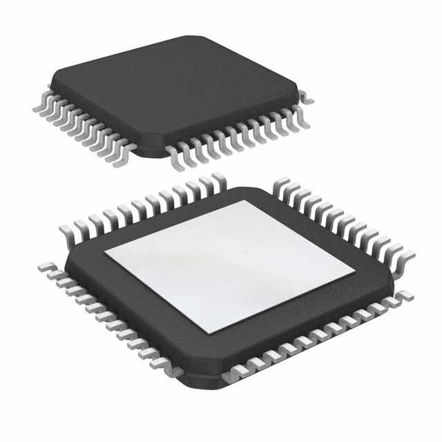
LXE Package
48-Lead Plastic Exposed Pad LQFP (7mm × 7mm)
(Reference LTC DWG #05-08-1927 Rev B)
Exposed Pad Variation AA
9.00 BSC
7.00 BSC
4.15 ±0.20
48
37
SEE NOTE: 3
1
48
37
36
36
1
9.00 BSC
7.00 BSC
4.15 ±0.20
A
A
12
25
25
12
C0.30 – 0.50
13
24
13
BOTTOM OF PACKAGE—EXPOSED PAD (SHADED AREA)
24
11° – 13°
1.35 – 1.45
R0.08 – 0.20
1.60
MAX
GAUGE PLANE
0.25
0° – 7°
LXE48 (AA) LQFP 0318 REV B
11° – 13°
0.09 – 0.20
1.00 REF
0.50
BSC
0.17 – 0.27
0.05 – 0.15
SIDE VIEW
0.45 – 0.75
SECTION A – A
NOTE:
1. DIMENSIONS ARE IN MILLIMETERS
2. DIMENSIONS OF PACKAGE DO NOT INCLUDE MOLD FLASH. MOLD FLASH
SHALL NOT EXCEED 0.25mm (10 MILS) BETWEEN THE LEADS AND ON ANY
SIDE OF EXPOSED PAD, MAX 0.50mm (20 MILS) AT CORNER OF EXPOSED
PAD, IF PRESENT
3. PIN-1 INDENTIFIER IS A MOLDED INDENTATION
4. DRAWING IS NOT TO SCALE
7.15 – 7.25
5.50 REF
1
48
37
36
0.50 BSC
5.50 REF
7.15 – 7.25
0.20 – 0.30
4.15 ±0.05
12
13
PACKAGE OUTLINE
24
25
COMPONENT
PIN “A1”
XXYY
LTCXXXX
4.15 ±0.05
1.30 MIN
RECOMMENDED SOLDER PAD LAYOUT
APPLY SOLDER MASK TO AREAS THAT ARE NOT SOLDERED
78
TRAY PIN 1
BEVEL
PACKAGE IN TRAY LOADING ORIENTATION
Rev A
For more information www.analog.com
�LTC2949
REVISION HISTORY
REV
DATE
DESCRIPTION
A
11/20
Changed GPOx to GPIOx.
PAGE NUMBER
Throughout
Moved Temperature Measurement into sub-section Application Information.
2
Adapted Abs Max of SDO.
3
Changed TYP value of VBYP2 in EC-table.
4
Changed Input Leakage current for CFPx from 40nA to 60nA.
Adapted ICC Average Supply Current in EC table and in text Modes of Operation.
4
4,15
Changed Input Leakage current for Voltage Measurement by Power ADC from 10nA to 60nA.
5
Symbol names corrections in EC table.
6
Changed Input Leakage current for Voltage Measurement by AUXILIARY ADC from 10nA to 60nA.
6
EC-Table External Clock Frequency adapted MIN value.
7
Adapted tlDLE MAX value.
8
Adapted VA Transmitter Pulse Amplitude MAX value.
8
Corrected symbol ATCMP in VICMP.
8
Corrected symbol VICM in ATCMP wrong.
8
Corrected Pin 6 missing in list of DNC-pins.
12
Core states vs fast conversions: Update of Figure 1.
15
Corrected wrong Figure 29.
16
Corrected wrong minimum frequency of 200kHz.
20
Corrected missing unit at first column of Table 3.
21
ISORPT still in register map table: Removed.
41
Register name typos: Corrected Register Map.
41
ADC limit behavior: Added sentence after Table 28.
48
Register name typos: Corrected Tables 71 and 72.
65, 66
Adapted Description of MUX[1-4]GC in Table 73.
66
Corrected Wrong Figure 1.
74
MOSFET polarities: Update of several transistor symbols.
77, 80
Rev A
Information furnished by Analog Devices is believed to be accurate and reliable. However, no responsibility is assumed by Analog
Devices for its use, nor for any infringements of patents or other rights of third parties that may result from its use. Specifications
subject to change without notice. No license For
is granted
implication or
otherwise under any patent or patent rights of Analog Devices.
more by
information
www.analog.com
79
�LTC2949
TYPICAL APPLICATION
Battery Metering with Low-Side Current & Charge Sensing, Battery Voltage Measurement,
Temperature Measurement, Contactor Supervision and Isolated Gate Drive of Pre-Charge FET.
VBAT+
LOAD OR CHARGER
RPRECH
STB9NK80Z
2M
20k
10µ
STB9NK80Z
V8/GP01
STB9NK80Z
1µ
2M
V9/GP02
VBAT–
VBATP
V10/GP03
10k
SPI/isoSPI
INTERFACE
BATTERY
VCC*
+
–
1µ
1µ
1µ
33p
1µ
VBATM
IOVCC
SCK/IP
CSB/IM
SDO/IBIAS
SDI/VCMP
DVCC
AVCC
V2
LTC2949
V4-V7
V12/GP05
10k
AGND
NTC
AGND
DGND
BYP1
VBAT–
NTCLE203E
V1
10k
VREF
10k
BYP2
V3
CLKO
4MHz
33p
STB9NK80Z
V11/GP04
CLKI
I2M CF2M CF2P I2P
I1M CF1M CF1P I1P
1µ
1µ
STB9NK80Z
2M
VBAT–
RSENSE
100µ
2949 TA02
*VCC SUPPLY VOLTAGE MUST BE CHOSEN TO ENSURE MINIMUM VGS OF USED MOSFETS UNDER ALL CONDITIONS.
RELATED PARTS
PART NUMBER
DESCRIPTION
COMMENTS
LTC6810-1/
LTC6810-2
4th Generation 6-Cell Battery Stack
Monitor and Balancing IC
Measures Cell Voltages for Up to 6 Series Battery Cells. The isoSPI Daisy-Chain
Capability Allows Multiple Devices to Be Interconnected for Measuring Many Battery
Cells Simultaneously. The isoSPI Bus Can Operate Up to 1MHz and Can Be Operated
Bidirectionally for Fault Conditions, Such as a Broken Wire or Connector. Includes
Internal Passive Cell Balancing Capability of Up to 150mA.
LTC6811-1/
LTC6811-2
4th Generation 12-Cell Battery Stack
Monitor and Balancing IC
Measures Cell Voltages for Up to 12 Series Battery Cells. Daisy-Chain Capability Allows
Multiple Devices to Be Connected to Measure Many Battery Cells Simultaneously Via the
Built-In 1MHz, 2-Wire Isolated Communication (isoSPI). Includes Capability for Passive
Cell Balancing.
LTC6820
isoSPI Isolated Communications Interface Provides an Isolated Interface for SPI Communication Up to 100 Meters, Using a Twisted
Pair. Companion to the LTC6804, LTC6806, LTC6811, LTC6812 and LTC6813
LTC6812-1
4th Generation 15-Cell Battery Stack
Monitor and Balancing IC
Measures Cell Voltages for Up to 15 Series Battery Cells. The isoSPI Daisy-Chain
Capability Allows Multiple Devices to Be Connected to Measuring Many Battery
Cells Simultaneously. The isoSPI Bus Can Operate Up to 1MHz and Can Be Operated
Bidirectionally for Fault Conditions, Such as a Broken Wire or Connector. Includes
Internal Passive Cell Balancing Capability of Up to 200mA.
LTC6813-1
4th Generation 18-Cell Battery Stack
Monitor and Balancing IC
Measures Cell Voltages for Up to 18 Series Battery Cells. The isoSPI Daisy-Chain
Capability Allows Multiple Devices to Be Interconnected for Measuring Many Battery
Cells Simultaneously. The isoSPI Bus Can Operate Up to 1MHz and Can Be Operated
Bidirectionally for Fault Conditions, Such as a Broken Wire or Connector. Includes
Internal Passive Cell Balancing Capability of Up to 200mA.
80
Rev A
11/20
www.analog.com
For more information www.analog.com
ANALOG DEVICES, INC. 2019-2020
�


 工商网监
湘ICP备2023018690号
工商网监
湘ICP备2023018690号

