LTC3025-1/LTC3025-2/
LTC3025-3/LTC3025-4
500mA Micropower
VLDO Linear Regulators
Features
n
n
n
n
n
n
n
n
n
n
n
n
n
n
n
Description
Wide Input Voltage Range: 0.9V to 5.5V
Stable with Ceramic Capacitors
Very Low Dropout: 85mV at 500mA
Adjustable Output Range: 0.4V to 3.6V (LTC3025-1)
Fixed Output: 1.2V (LTC3025-2), 1.5V (LTC3025-3),
1.8V (LTC3025-4)
±2% Voltage Accuracy over Temperature,
Supply and Load
Low Noise: 80µVRMS (10Hz to 100kHz)
BIAS Voltage Range: 2.5V to 5.5V
Fast Transient Recovery
Shutdown Disconnects Load from VIN and VBIAS
Low Operating Current: IIN = 4µA, IBIAS = 50µA Typ
Low Shutdown Current: IIN = 1µA, IBIAS = 0.01µA Typ
Output Current Limit
Thermal Overload Protection
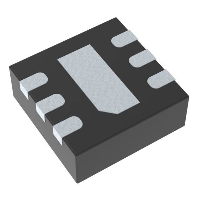
Available in 6-Lead (2mm × 2mm) DFN Package
Applications
n
n
n
n
n
n
n
Low Power Handheld Devices
Low Voltage Logic Supplies
DSP Power Supplies
Cellular Phones
Portable Electronic Equipment
Handheld Medical Instruments
Post Regulator for Switching Supply Noise Rejection
The LTC®3025-X is a micropower, VLDO™ (very low dropout) linear regulator which operates from input voltages as
low as 0.9V. The device is capable of supplying 500mA of
output current with a typical dropout voltage of only 85mV.
A BIAS supply is required to run the internal reference and
LDO circuitry while output current comes directly from the
IN supply for high efficiency regulation. The LTC3025-1
features an adjustable output with a low 0.4V reference
while the LTC3025-2, LTC3025-3, and LTC3025-4 have
fixed 1.2V, 1.5V and 1.8V output voltages respectively.
The LTC3025-X’s low quiescent current makes it an ideal
choice for use in battery-powered systems. For 3-cell NiMH
and single cell Li-Ion applications, the BIAS voltage can
be supplied directly from the battery while the input can
come from a high efficiency buck regulator, providing a
high efficiency, low noise output.
Other features include high output voltage accuracy,
excellent transient response, stability with ultralow ESR
ceramic capacitors as small as 1µF, short-circuit and
thermal overload protection and output current limiting.
The LTC3025-X is available in a tiny, low profile (0.75mm)
6-lead DFN (2mm × 2mm) package.
L, LT, LTC, LTM, Linear Technology and the Linear logo are registered trademarks and VLDO
and ThinSOT are trademarks of Linear Technology Corporation. All other trademarks are the
property of their respective owners. Protected by U.S. Patents including 7224204, 7218082.
Typical Application
1MHz VIN Supply Rejection
1.2V Output Voltage from 1.5V Input Supply
50
45
BIAS
1.5V HIGH
EFFICIENCY 1.5V
DC/DC
BUCK
0.1µF
1µF
LTC3025-2
IN
SENSE
0.1µF
OFF ON
SHDN
VOUT = 1.2V
IOUT ≤ 500mA
GND
30251234 TA01
COUT = 10µF
40
REJECTION (dB)
Li-Ion
OR
3-CELL
NiMH
OUT
35
COUT = 1µF
30
25
20
15
10
5 BIAS = 3.6V
VOUT = 1.2V
0
1.2 1.4 1.6
IOUT = 100mA
IOUT = 300mA
1.8 2.0
VIN (V)
2.2
2.4
2.6
30251234 TA01b
30251234ff
1
�LTC3025-1/LTC3025-2/
LTC3025-3/LTC3025-4
Absolute Maximum Ratings
Pin Configuration
(Notes 1, 2)
VBIAS, VIN to GND.......................................... –0.3V to 6V
SHDN to GND................................................ –0.3V to 6V
SENSE, ADJ to GND...................................... –0.3V to 6V
VOUT.........................................–0.3V to VIN + 0.3V or 6V
Operating Junction Temperature Range
(Note 3)................................................... –40°C to 125°C
Storage Temperature Range.................... –65°C to 125°C
Output Short-Circuit Duration........................... Indefinite
TOP VIEW
BIAS 1
GND 2
6 SHDN
7
IN 3
5 ADJ/SENSE*
4 OUT
DC6 PACKAGE
6-LEAD (2mm × 2mm) PLASTIC DFN
TJMAX = 125°C, θJA = 102°C/W, θJC = 20°C/W
EXPOSED PAD (PIN 7) IS GND, MUST BE SOLDERED TO PCB
*ADJ FOR LTC3025-1, SENSE FOR LTC3025-2, LTC3025-3, LTC3025-4
order information
LEAD FREE FINISH
TAPE AND REEL
PART MARKING*
PACKAGE DESCRIPTION
TEMPERATURE RANGE
LTC3025EDC-1#PBF
LTC3025EDC-1#TRPBF
LDDW
6-Lead (2mm × 2mm) Plastic DFN
–40°C to 125°C
LTC3025IDC-1#PBF
LTC3025IDC-1#TRPBF
LDDW
6-Lead (2mm × 2mm) Plastic DFN
–40°C to 125°C
LTC3025EDC-2#PBF
LTC3025EDC-2#TRPBF
LDMK
6-Lead (2mm × 2mm) Plastic DFN
–40°C to 125°C
LTC3025IDC-2#PBF
LTC3025IDC-2#TRPBF
LDMK
6-Lead (2mm × 2mm) Plastic DFN
–40°C to 125°C
LTC3025EDC-3#PBF
LTC3025EDC-3#TRPBF
LDQS
6-Lead (2mm × 2mm) Plastic DFN
–40°C to 125°C
LTC3025IDC-3#PBF
LTC3025IDC-3#TRPBF
LDQS
6-Lead (2mm × 2mm) Plastic DFN
–40°C to 125°C
LTC3025EDC-4#PBF
LTC3025EDC-4#TRPBF
LDPQ
6-Lead (2mm × 2mm) Plastic DFN
–40°C to 125°C
LTC3025IDC-4#PBF
LTC3025IDC-4#TRPBF
LDPQ
6-Lead (2mm × 2mm) Plastic DFN
–40°C to 125°C
LEAD BASED FINISH
TAPE AND REEL
PART MARKING*
PACKAGE DESCRIPTION
TEMPERATURE RANGE
LTC3025EDC-1
LTC3025EDC-1#TR
LDDW
6-Lead (2mm × 2mm) Plastic DFN
–40°C to 125°C
LTC3025IDC-1
LTC3025IDC-1#TR
LDDW
6-Lead (2mm × 2mm) Plastic DFN
–40°C to 125°C
LTC3025EDC-2
LTC3025EDC-2#TR
LDMK
6-Lead (2mm × 2mm) Plastic DFN
–40°C to 125°C
LTC3025IDC-2
LTC3025IDC-2#TR
LDMK
6-Lead (2mm × 2mm) Plastic DFN
–40°C to 125°C
LTC3025EDC-3
LTC3025EDC-3#TR
LDQS
6-Lead (2mm × 2mm) Plastic DFN
–40°C to 125°C
LTC3025IDC-3
LTC3025IDC-3#TR
LDQS
6-Lead (2mm × 2mm) Plastic DFN
–40°C to 125°C
LTC3025EDC-4
LTC3025EDC-4#TR
LDPQ
6-Lead (2mm × 2mm) Plastic DFN
–40°C to 125°C
LTC3025IDC-4
LTC3025IDC-4#TR
LDPQ
6-Lead (2mm × 2mm) Plastic DFN
–40°C to 125°C
Consult LTC Marketing for parts specified with wider operating temperature ranges. *The temperature grade is identified by a label on the shipping container.
For more information on lead free part marking, go to: http://www.linear.com/leadfree/
For more information on tape and reel specifications, go to: http://www.linear.com/tapeandreel/
30251234ff
2
�LTC3025-1/LTC3025-2/
LTC3025-3/LTC3025-4
Electrical
Characteristics
The
l denotes the specifications which apply over the full operating
temperature range, otherwise specifications are at TA = 25°C. VIN = 1.5V, VBIAS = 3.6V, COUT = 1µF, CIN = 0.1µF, CBIAS = 0.1µF
(all capacitors ceramic) unless otherwise noted. (Note 3)
PARAMETER
CONDITIONS
VIN Operating Voltage (Note 4)
LTC3025-1
l
0.9
5.5
V
LTC3025-2
l
1.4
5.5
V
LTC3025-3
l
1.7
5.5
V
LTC3025-4
l
2.0
5.5
V
LTC3025-1
l
2.5
5.5
V
LTC3025-2
l
2.7
5.5
V
LTC3025-3
l
3.0
5.5
V
LTC3025-4
l
3.3
5.5
V
VBIAS Operating Voltage (Note 4)
VBIAS Undervoltage Lockout
MIN
TYP
MAX
UNITS
l
2.2
2.5
V
VIN Operating Current
IOUT = 10µA, VOUT = 1.2V, LTC3025-1
l
4
10
µA
VIN Operating Current
IOUT = 0µA, LTC3025-2/LTC3025-3/LTC3025-4
l
4
10
µA
50
80
µA
50
80
µA
VBIAS Operating Current
IOUT = 10µA, VOUT = 1.2V, LTC3025-1
l
VBIAS Operating Current
IOUT = 0µA, LTC3025-2/LTC3025-3/LTC3025-4
l
VIN Shutdown Current
VSHDN = 0V
1
5
µA
VBIAS Shutdown Current
VSHDN = 0V
0.01
1
µA
VADJ Regulation Voltage (Note 5)
1mA ≤ IOUT ≤ 500mA, VOUT = 1.2V, 1.5V ≤ VIN ≤ 5V, LTC3025-1
1mA ≤ IOUT ≤ 500mA, VOUT = 1.2V, 1.5V ≤ VIN ≤ 5V, LTC3025-1
l
0.395
0.392
0.4
0.4
0.405
0.408
V
V
1mA ≤ IOUT ≤ 500mA, 1.5V ≤ VIN ≤ 5V, LTC3025-2
1mA ≤ IOUT ≤ 500mA, 1.5V ≤ VIN ≤ 5V, LTC3025-2
l
1.185
1.176
1.2
1.2
1.215
1.224
V
V
1mA ≤ IOUT ≤ 500mA, 1.7V ≤ VIN ≤ 5V, LTC3025-3
1mA ≤ IOUT ≤ 500mA, 1.7V ≤ VIN ≤ 5V, LTC3025-3
l
1.481
1.470
1.5
1.5
1.519
1.530
V
V
1mA ≤ IOUT ≤ 500mA, 2.0V ≤ VIN ≤ 5V, LTC3025-4
1mA ≤ IOUT ≤ 500mA, 2.0V ≤ VIN ≤ 5V, LTC3025-4
l
1.777
1.764
1.8
1.8
1.823
1.836
V
V
–50
0
50
nA
VSENSE Regulation Voltage (Note 5)
VSENSE Regulation Voltage (Note 5)
VSENSE Regulation Voltage (Note 5)
IADJ ADJ Input Current
VADJ = 0.45V, LTC3025-1
OUT Load Regulation (Referred to ADJ Pin) ∆IOUT = 1mA to 500mA, LTC3025-1
–0.35
mV
OUT Load Regulation
∆IOUT = 1mA to 500mA, LTC3025-2
∆IOUT = 1mA to 500mA, LTC3025-3
∆IOUT = 1mA to 500mA, LTC3025-4
–1
–1.3
–1.5
mV
mV
mV
VIN Line Regulation (Referred to ADJ Pin)
VIN = 1.5V to 5V, VBIAS = 3.6V, VOUT = 1.2V,
IOUT = 1mA, LTC3025-1
0.07
mV
VIN Line Regulation
VIN = 1.5V to 5V, VBIAS = 3.6V, IOUT = 1mA, LTC3025-2
VIN = 1.8V to 5V, VBIAS = 3.6V, IOUT = 1mA, LTC3025-3
VIN = 2.1V to 5V, VBIAS = 3.6V, IOUT = 1mA, LTC3025-4
0.21
0.26
0.32
mV
mV
mV
VBIAS Line Regulation
VIN = 1.5V, VBIAS = 2.7V to 5V, VOUT = 1.2V, IOUT = 1mA,
LTC3025-1
l
4.5
16.5
mV
VBIAS Line Regulation
VIN = 1.5V, VBIAS = 2.7V to 5V, IOUT = 1mA, LTC3025-2
VIN = 1.8V, VBIAS = 3.0V to 5V, IOUT = 1mA, LTC3025-3
VIN = 2.1V, VBIAS = 3.3V to 5V, IOUT = 1mA, LTC3025-4
l
l
l
4.5
4.5
4.5
16.5
16.5
16.5
mV
mV
mV
VIN to VOUT Dropout Voltage (Notes 4, 6)
VBIAS = 3V, VIN = 1.5V, IOUT = 500mA,
VADJ = 0.37V(LTC3025-1), VSENSE = 1.15V(LTC3025-2)
85
l
120
170
mV
mV
VBIAS = 3.1V, VIN = 1.7V, IOUT = 500mA,
VSENSE = 1.45V(LTC3025-3)
90
l
130
185
mV
mV
VBIAS = 3.4V, VIN = 2.0V, IOUT = 500mA,
VSENSE = 1.75V(LTC3025-4)
90
l
130
185
mV
mV
LTC3025-1
l
1.5
V
VIN to VOUT Dropout Voltage (Notes 4, 6)
VIN to VOUT Dropout Voltage (Notes 4, 6)
VBIAS to VOUT Dropout Voltage (Note 4)
30251234ff
3
�LTC3025-1/LTC3025-2/
LTC3025-3/LTC3025-4
ELECTRICAL CHARACTERISTICS
The l denotes the specifications which apply over the full operating
temperature range, otherwise specifications are at TA = 25°C. VIN = 1.5V, VBIAS = 3.6V, COUT = 1µF, CIN = 0.1µF, CBIAS = 0.1µF
(all capacitors ceramic) unless otherwise noted. (Note 3)
PARAMETER
CONDITIONS
MIN
IOUT Continuous Output Current
l
IOUT Current Limit
VADJ = 0V(LTC3025-1),
VSENSE = 0V(LTC3025-2/LTC3025-3/LTC3025-4)
en Output Voltage Noise
f = 10Hz to 100kHz, IOUT = 300mA
TYP
MAX
500
mA
1130
mA
80
VIH SHDN Input High Voltage
l
VIL SHDN Input Low Voltage
l
UNITS
µVRMS
0.9
V
0.3
V
IIH SHDN Input High Current
SHDN = 1.2V
–1
1
µA
IL SHDN Input Low Current
SHDN = 0V
–1
1
µA
Note 1: Stresses beyond those listed under Absolute Maximum Ratings
may cause permanent damage to the device. Exposure to any Absolute
Maximum Rating condition for extended periods may affect device
reliability and lifetime.
Note 2: This IC includes overtemperature protection that is intended
to protect the device during momentary overload conditions. Junction
temperature will exceed 125°C when overtemperature protection is active.
Continuous operation above the specified maximum operating junction
temperature may impair device reliability.
Note 3: The LTC3025-X regulators are tested and specified under pulse
load conditions such that TJ ≈ TA. The LTC3025E-X are guaranteed to
meet performance specifications from 0°C and 125°C. Specifications over
the –40°C to 125°C operating junction temperature range are assured by
design, characterization and correlation with statistical process controls.
The LTC3025I-X are guaranteed to meet performance specifications over
the full –40°C to 125°C operating junction temperature range.
Note 4: For the LTC3025-1, a regulated output voltage will only be available
when the minimum IN and BIAS operating voltages as well as the IN to
OUT and BIAS to OUT dropout voltages are all satisfied. For the
LTC3025-2/LTC3025-3/LTC3025-4 the minimum IN operating voltage
assumes IOUT = 500mA. For correct regulation at IOUT < 500mA the
minimum IN operating voltage decreases to the maximum VSENSE
Regulation Voltage as IOUT decreases to 0mA (i.e. VINMIN = 1.312V at IOUT
= 250mA for the LTC3025-2).
Note 5: Operating conditions are limited by maximum junction
temperature. The regulated output voltage specification will not apply
for all possible combinations of input voltage and output current. When
operating at maximum input voltage, the output current range must be
limited. When operating at maximum output current, the input voltage
range must be limited.
Note 6: Dropout voltage is minimum input to output voltage differential
needed to maintain regulation at a specified output current. In dropout, the
output voltage will be equal to VIN – VDROPOUT.
30251234ff
4
�LTC3025-1/LTC3025-2/
LTC3025-3/LTC3025-4
Typical Performance Characteristics
VIN to VOUT Dropout Voltage
vs IOUT
DROPOUT VOLTAGE (mV)
100
Operating BIAS Current
vs Output Current
VBIAS = 2.8V
VIN = 1.4V
VIN = 1.5V
70 VOUT = 1.2V
400
TA = 25°C
IBIAS (µA)
TA = –40°C
40
60
350
60
300
125°C
250
25°C
200
–40°C
150
0
0.01
50 100 150 200 250 300 350 400 450 500
IOUT (mA)
0.1
1
100
10
IOUT (mA)
85°C
25°C
VBIAS = 5V
404
403
–40°C
–40°C
4
3
25°C
4
2
2
1
0
0.5
0
0.5
1.5
2.5
3.5
4.5
5.5
1600
900
1400
CURRENT LIMIT (mA)
SHDN THRESHOLD (mV)
800
600
VBIAS = 2.5V
500
400
300
200
1.5
2.5
3.5
4.5
5.5
–25
50
25
0
75
TEMPERATURE (°C)
401
400
399
398
395
–50
–25
100
125
30251234 G07
50
25
0
75
TEMPERATURE (°C)
100
125
30251234 G06
Burst Mode DC/DC Buck Ripple
Rejection
Current Limit vs VIN Voltage
VIN
AC
100mV/DIV
1200
1000
800
VOUT
AC
10mV/DIV
600
400
200
100
0
–50
402
30251234 G05
1000
5.5
396
30251234 G04
SHDN Threshold vs Temperature
5
VBIAS = 3.6V
VIN = 1.5V
IOUT = 10µA
VIN (V)
VBIAS = 5V
4.5
4
VBIAS (V)
397
85°C
VIN (V)
700
3.5
Adjust Voltage vs Temperature
ADJUST VOLTAGE (mV)
8
3
30251234 G03
405
5
125°C
6
0
2.5
1000
6
IIN (µA)
IIN (µA)
7
VBIAS = 5V
VOUT = 0.8V
10
30
VIN Shutdown Current
VIN No Load Operating Current
12
25°C
30251234 G02
30251234 G01
14
–40°C
40
10
50
0
125°C
50
20
100
20
0
80
450
TA = 125°C
80
BIAS No Load Operating Current
500
IBIAS (µA)
120
(TA = 25°C unless otherwise noted)
0
0
1
2
3
VIN (V)
4
5
6
VIN = 1.8V
VOUT = 1.5V
COUT = 1µF
IOUT = 50mA
10µs/DIV
30251234 G09
30251234 G08
30251234ff
5
�LTC3025-1/LTC3025-2/
LTC3025-3/LTC3025-4
Typical Performance Characteristics
BIAS Ripple Rejection
vs Frequency
70
70
60
60
50
40
COUT = 1µF
30
20
10
50
50
40
30
COUT = 1µF
20
VBIAS = 3.6V
VIN = 1.5V
VOUT = 1.2V
IOUT = 100mA
0
100
1k
VBIAS = 3.6V
VIN = 1.5V
VOUT = 1.2V
IOUT = 100mA
10
10k
100k
1M
0
100
10M
3MHz VIN Supply Rejection
45
COUT = 10µF
REJECTION (dB)
COUT = 10µF
REJECTION (dB)
REJECTION (dB)
VIN Ripple Rejection
vs Frequency
(TA = 25°C unless otherwise noted)
1k
40
COUT = 10µF
35
COUT = 1µF
30
25
20
15
10
10k
100k
5 VBIAS = 3.6V
VOUT = 1.2V
0
1.2 1.4 1.6
10M
1M
FREQUENCY (Hz)
FREQUENCY (Hz)
IOUT = 100mA
IOUT = 300mA
1.8 2.0
VIN (V)
2.2
2.4
2.6
30251234 G12
30251234 G11
30251234 G10
Transient Response
0.300
0.300
BIAS = 2.7V
0.275
250mA
0.250
0.225
VOUT
AC
10mV/DIV
0.175
0.150
BIAS = 3.8V
0.125
0.100
0.075
VIN = 1.5V
VOUT = 1.2V
VBIAS = 3.6V
COUT = 1µF
100µs/DIV
30251234 G13
0.225
BIAS = 3.3V
BIAS = 3V
0.200
DROPOUT (V)
10mA
BIAS = 5V
VADJ = 0.385
IOUT = 500mA
TA = 25°C
0.050
0.025
0
VIN to VOUT Dropout Voltage
vs VIN (90°C) LTC3025-1
0.275
0.250
DROPOUT (V)
IOUT
VIN to VOUT Dropout Voltage
vs VIN (25°C) LTC3025-1
1
1.5
2
3
2.5
VIN (V)
3.5
4
4.5
30251234 G14
0.200
0.175
0.150
BIAS = 3.8V
0.125
BIAS = 5V
0.100
0.075
BIAS = 3.3V
VADJ = 0.385
BIAS = 3V
IOUT = 500mA
BIAS = 2.7V
TA = 90°C
0.050
0.025
0
1
1.5
2
3
2.5
VIN (V)
3.5
4
4.5
30251234 G15
30251234ff
6
�LTC3025-1/LTC3025-2/
LTC3025-3/LTC3025-4
Pin Functions
BIAS (Pin 1): BIAS Input Voltage. BIAS provides internal
power for LTC3025-X circuitry. The BIAS pin should be
locally bypassed to ground if the LTC3025-X is more than a
few inches away from another source of bulk capacitance.
In general, the output impedance of a battery rises with
frequency, so it is usually advisable to include an input
bypass capacitor in battery-powered circuits. A capacitor
in the range of 0.01µF to 0.1µF is usually sufficient.
GND (Pin 2): Ground. Connect to a ground plane.
IN (Pin 3): Input Supply Voltage. The output load current
is supplied directly from IN. The IN pin should be locally
bypassed to ground if the LTC3025-X is more than a few
inches away from another source of bulk capacitance.
In general, the output impedance of a battery rises with
frequency, so it is usually advisable to include an input
bypass capacitor when supplying IN from a battery. A
capacitor in the range of 0.1µF to 1µF is usually sufficient.
OUT (Pin 4): Regulated Output Voltage. The OUT pin
supplies power to the load. A minimum ceramic output
capacitor of at least 1µF is required to ensure stability.
Larger output capacitors may be required for applications
with large transient loads to limit peak voltage transients.
See the Applications Information section for more information on output capacitance.
ADJ (Pin 5) LTC3025-1: Adjust Input. This is the input to
the error amplifier. The ADJ pin reference voltage is 0.4V
referenced to ground. The output voltage range is 0.4V to
3.6V and is typically set by connecting ADJ to a resistor
divider from OUT to GND. See Figure 2.
SENSE (Pin 5) LTC3025-2, LTC3025-3, LTC3025-4: Output
Sense. The sense is the input to the resistor divider driving
the error amplifier. Optimum regulation will be obtained at
the point where SENSE is connected to OUT. The SENSE pin
bias current is 10µA at the nominal rated output voltage.
SHDN (Pin 6): Shutdown Input, Active Low. This pin is
used to put the LTC3025-X into shutdown. The SHDN pin
current is typically less than 10nA. The SHDN pin cannot
be left floating and must be tied to a valid logic level (such
as BIAS) if not used.
GND (Exposed Pad Pin 7): Ground and Heat Sink. Must
be soldered to PCB ground plane or large pad for optimal
thermal performance.
Block Diagram
LTC3025-1
1
6
LTC3025-2, LTC3025-3, LTC3025-4
BIAS
SHDN
1
REFERENCE
SHDN
0.4V
SOFT-START
IN
+
–
2
GND
6µA
3
6
BIAS
SHDN
REFERENCE
SHDN
0.4V
SOFT-START
IN
+
–
OUT
ADJ
4
5
2
6µA
OUT
GND
SENSE
R1
40k
R2
80k (LTC3025-2)
110k (LTC3025-3)
140k (LTC3025-4)
3
4
5
30251234 BD
30251234ff
7
�LTC3025-1/LTC3025-2/
LTC3025-3/LTC3025-4
Applications Information
Operation (Refer to Block Diagram)
Adjustable Output Voltage (LTC3025-1)
The LTC3025-X is a micropower, VLDO (very low dropout)
linear regulator which operates from input voltages as low
as 0.9V. The device provides a highly accurate output that
is capable of supplying 500mA of output current with a
typical dropout voltage of only 85mV. A single ceramic
capacitor as small as 1µF is all that is required for output
bypassing. A low reference voltage allows the LTC3025-1
output to be programmed to much lower voltages than
available in common LDOs (range of 0.4V to 3. 6V). The
LTC3025-2/LTC3025-3/LTC3025-4 have fixed outputs of
1.2V, 1.5V and 1.8V respectively, eliminating the need for
an external resistor divider.
The output voltage is set by the ratio of two external resistors as shown in Figure 2. The device servos the output
to maintain the ADJ pin voltage at 0.4V (referenced to
ground). Thus, the current in R1 is equal to 0.4V/R1. For
good transient response, stability, and accuracy, the current
in R1 should be at least 8µA, thus the value of R1 should
be no greater than 50k. The current in R2 is the current in
R1 plus the ADJ pin bias current. Since the ADJ pin bias
current is typically


 工商网监
湘ICP备2023018690号
工商网监
湘ICP备2023018690号

