LTC3209-1/LTC3209-2
600mA Main/Camera
LED Controller
DESCRIPTIO
U
FEATURES
■
■
Multimode Charge Pump Provides Up to 94%
Efficiency (1x, 1.5x, 2x)
Up to 600mA Total Output Current
LTC3209-1: 8 Current Sources Available as
6 × 25mA MAIN, 1 × 400mA CAM and 1 × 15mA AUX
LTC3209-2: 8 Current Sources Available as
5 × 25mA MAIN, 2 × 200mA CAM and 1 × 15mA AUX
LED On/Off and Brightness Level Programmable
Using 2-Wire I2CTM Interface
Automatic Charge Pump Mode Switching or Fixed
Mode for Power Supply Generation
Low Noise Constant Frequency Operation*
Internal Soft-Start Limits Inrush Current During
Start-up and Mode Switching
Short Circuit/Thermal/Open-Shorted LED Protection
256 Brightness States for MAIN Display
16 Brightness States for CAM Display
4 Brightness States for AUX Display
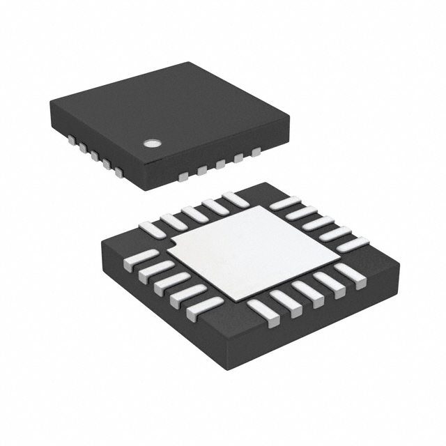
20-Lead (4mm × 4mm) QFN Package
■
Video/Camera Phones with QVGA+ Displays
■
■
■
■
■
■
■
■
■
■
■
U
APPLICATIO S
, LT, LTC and LTM are registered trademarks of Linear Technology Corporation.
All other trademarks are the property of their respective owners.
*Protected by U.S. Patents, including 6411531
The LTC ®3209-1/LTC3209-2 are highly integrated
multidisplay LED controllers. These parts contain a high
efficiency, low noise charge pump to provide power to
MAIN, CAM and AUX LED displays. The LTC3209-1/
LTC3209-2 require only four small ceramic capacitors
and one current set resistor to form a complete LED power
supply and current controller.
The maximum display currents are set by a single external
resistor. Current for each LED is controlled by a precision
internal current source. Dimming and On/Off for all displays is achieved via the I2C serial interface. 256 states are
available for the MAIN display. Sixteen states are available
for the CAM display and four states are available for the
AUX display.
The charge pump optimizes efficiency based on the
voltage across the LED current sources. The part powers
up in 1x mode and will automatically switch to boost mode
whenever any enabled MAIN or CAM LED current source
begins to enter dropout. The first dropout switches the
part into 1.5x mode and a subsequent dropout switches
the part into 2x mode. The part resets to 1x mode
whenever a data bit is updated via the I2C port. The parts
are available in a 4mm × 4mm 20-lead QFN package.
U
TYPICAL APPLICATIO
LTC3209-1 6 MAIN/1 CAM Operation
2.2µF
2.2µF
C1P C1M C2P C2M
VBAT
LTC3209-2 5 MAIN/2 CAM Operation
2.2µF
2.2µF
MAIN
CAM
C1P C1M C2P C2M
VBAT
CPO
VBAT1,2
RED
2.2µF
24.3k
RED
SCL
I2C
6
CAMHL
RREF
CAM
LTC3209-2
MAIN1-6
5
SDA
CAM
LOW HI
MAIN
2.2µF
SCL
SDA
2.2µF
CPO
VBAT1,2
LTC3209-1
I2C
2.2µF
AUX
GND
MAIN1-5
CAM
3209 TA01
LOW HI
CAMHL
RREF
AUX
GND
2
3209 TA02
24.3k
320912fa
1
�LTC3209-1/LTC3209-2
W W
U
W
ABSOLUTE
AXI U RATI GS
(Note 1)
VBAT, DVCC, CPO to GND ............................... –0.3 to 6V
SDA, SCL, CAMHL ..................... –0.3V to (DVCC + 0.3V)
ICPO (Note 4)....................................................... 700mA
IMAIN1-6 (Note 5) ................................................... 31mA
IAUX (Note 5) ......................................................... 30mA
ICAM1-2 (Note 5) .................................................. 250mA
ICAM (Note 5) ...................................................... 500mA
CPO, RREF Short-Circuit Duration ....................Indefinite
Operating Temperature Range (Note 2) .. –40°C to 85°C
Storage Temperature Range ................. –65°C to 125°C
U
W
U
PACKAGE/ORDER I FOR ATIO
13 CAMHL
MAIN2 3
MAIN3 4
12 CAM
MAIN3 4
MAIN4 5
11 DVCC
MAIN4 5
7
8
9 10
MAIN5
MAIN6
AUX
VBAT2
RREF
6
C2M
C1M
15 SCL
14 SDA
13 CAMHL
21
12 CAM2
11 CAM1
6
7
8
9 10
DVCC
MAIN1 2
RREF
14 SDA
VBAT2
MAIN1 2
21
VBAT1
C1P
CPO 1
AUX
15 SCL
MAIN5
C1M
VBAT1
C2P
C1P
C2M
20 19 18 17 16
20 19 18 17 16
CPO 1
MAIN2 3
C2P
TOP VIEW
TOP VIEW
UF PACKAGE
20-LEAD (4mm × 4mm) PLASTIC QFN
UF PACKAGE
20-LEAD (4mm ´ 4mm) PLASTIC QFN
TJMAX = 125°C, θJA = 40°C/W
EXPOSED PAD IS GND (PIN 21), MUST BE SOLDERED TO PCB
TJMAX = 125°C, θJA = 40°C/W
EXPOSED PAD IS GND (PIN 21), MUST BE SOLDERED TO PCB
ORDER PART NUMBER
UF PART MARKING
ORDER PART NUMBER
UF PART MARKING
LTC3209EUF-1
32091
LTC3209EUF-2
32092
Order Options Tape and Reel: Add #TR
Lead Free: Add #PBF Lead Free Tape and Reel: Add #TRPBF
Lead Free Part Marking: http://www.linear.com/leadfree/
Consult LTC Marketing for parts specified with wider operating temperature ranges.
ELECTRICAL CHARACTERISTICS
The ● denotes the specifications which apply over the full operating
temperature range, otherwise specifications are at TA = 25°C. VBAT1,2 = 3.6V, DVCC = 3V, RREF = 24.3k, C1 = C2 = C3 = C4 = 2.2µF,
unless otherwise noted.
PARAMETER
CONDITIONS
●
VBAT Operating Voltage
IVBAT Operating Current
MIN
2.9
ICPO = 0, 1x Mode, LED Disabled
ICPO = 0, 1.5x Mode
ICPO = 0, 2x Mode
VBAT UVLO Threshold
●
DVCC Operating Voltage
DVCC Operating Current
DVCC = 1.8V, Serial Port Idle
MAX
4.5
●
V
mA
mA
mA
1.5
V
1.5
4.5
V
1
µA
1
DVCC = 3V
UNITS
0.4
2.7
4.5
●
DVCC UVLO Threshold
VBAT Shutdown Current
TYP
3
V
7
µA
320912fa
2
�LTC3209-1/LTC3209-2
ELECTRICAL CHARACTERISTICS
The ● denotes the specifications which apply over the full operating
temperature range, otherwise specifications are at TA = 25°C. VBAT1,2 = 3.6V, DVCC = 3V, RREF = 24.3k, C1 = C2 = C3 = C4 = 2.2µF,
unless otherwise noted.
PARAMETER
White LED Current (MAIN1-6), 8-Bit Linear DAC
CONDITIONS
Full-Scale LED Current
MAIN = 1V
Minimum (1LSB) LED Current
MAIN = 1V
LED Current Matching
Any Two MAIN Outputs at 50% FS
LED Dropout Voltage
Mode Switch Threshold, IMAINx = FS
MIN
●
25
TYP
MAX
28
31
UNITS
mA
µA
110
1
%
180
mV
White LED Current (CAM), LTC3209-1, 4-Bit Linear DAC
Full-Scale LED Current
CAM = 1V
Minimum (1LSB) LED Current
CAM = 1V
●
360
LED Dropout Voltage
Mode Switch Threshold, ICAM = FS
White LED Current (CAM1-2), LTC3209-2, 4-Bit Linear DAC
Full-Scale LED Current
CAM = 1V
Minimum (1LSB) LED Current
CAM = 1V
LED Current Matching
CAM1-2 at 50% FS
LED Dropout Voltage
Mode Switch Threshold, ICAM = FS
●
180
400
440
mA
26.8
mA
400
mV
200
220
mA
13.3
mA
1
%
400
mV
AUX LED Current, 2-Bit Linear DAC
●
Full-Scale LED Current
AUX = 1V
12.5
13.75
15
mA
Minimum (1LSB) LED Current
AUX = 1V
4.4
mA
VOL
IAUX = 1mA; C0, C1 = High
18
mV
1x Mode Output Impedance
1.5x Mode Output Impedance
VBAT = 3V, VCPO = 4.2V (Note 3)
0.5
2.7
Ω
Ω
2x Mode Output Impedance
VBAT = 3V, VCPO = 4.8V (Note 3)
3.2
Ω
CPO Voltage Regulation
1.5x Mode, ICPO = 2mA
2x Mode, ICPO = 2mA
4.6
5.1
V
V
0.85
MHz
Charge Pump (CPO)
CLOCK Frequency
SDA, SCL, CAMHL
VIL (Low Level Input Voltage)
●
VIH (High Level Input Voltage)
●
0.3 • DVCC
V
0.4
V
0.7 • DVCC
V
VOL, Digital Output Low (SDA)
IPULLUP = 3mA
●
IIH
SDA, SCL, CAMHL = DVCC
●
–1
1
µA
IIL
SDA, SCL, CAMHL = 0V
●
–1
1
µA
400
kHz
0.16
Serial Port Timing (Notes 6, 7)
tSCL
Clock Operating Frequency
tBUF
Bus Free Time Between Stop and Start Condition
1.3
µs
tHD,STA
Hold Time After (Repeated) Start Condition
0.6
µs
tSU,STA
Repeated Start Condition Setup Time
0.6
µs
tSU,STO
tHD,DAT(OUT)
Stop Condition Setup Time
Data Hold Time
0.6
0
tHD,DAT(IN)
Input Data Hold Time
tSU,DAT
tLOW
tHIGH
tf
tr
900
µs
ns
0
ns
Data Setup Time
100
ns
Clock Low Period
1.3
µs
Clock High Period
Clock Data Fall Time
Clock Data Rise Time
0.6
20
20
300
300
µs
ns
ns
320912fa
3
�LTC3209-1/LTC3209-2
ELECTRICAL CHARACTERISTICS
The ● denotes the specifications which apply over the full operating
temperature range, otherwise specifications are at TA = 25°C. VBAT1,2 = 3.6V, DVCC = 3V, RREF = 24.3k, C1 = C2 = C3 = C4 = 2.2µF,
unless otherwise noted.
PARAMETER
tSP
RREF
VRREF
RRREF
CONDITIONS
Spike Suppression Time
●
RREF = 24.3k
Reference Resistor Range
Note 1: Stresses beyond those listed under Absolute Maximum Ratings
may cause permanent damage to the device. Exposure to any Absolute
Maximum Rating condition for extended periods may affect device
reliability and lifetime.
Note 2: The LTC3209-1/LTC3209-2 are guaranteed to meet performance
specifications from 0°C to 70°C. Specifications over the –40°C to 85°C
ambient operating temperature range are assured by design,
characterization and correlation with statistical process controls.
MIN
50
TYP
MAX
UNITS
ns
1.20
20
1.23
1.26
30
V
kΩ
Note 3: 1.5x mode output impedance is defined as (1.5VBAT – VCPO)/IOUT.
2x mode output impedance is defined as (2VBAT – VCPO)/IOUT.
Note 4: Based on long term current density limitations. Assumes an
operating duty cycle of ≤ 10% under absolute maximum conditions for
duration less than 10 seconds. Max Charge Pump current for continuous
operation is 300mA.
Note 5: Based on long term current density limitations.
Note 6: All values are referrenced to VIH and VIL levels.
Note 7: Guaranteed by design.
U W
TYPICAL PERFOR A CE CHARACTERISTICS TA = 25°C unless otherwise noted
Mode Switch Fast Dropout Times
1.5x Mode CPO Ripple
2x Mode CPO Ripple
2x
1.5x
1x
VCPO
20mV/DIV
AC COUPLED
VCPO
1V/DIV
VCPO
20mV/DIV
AC COUPLED
320912 G01
1ms/DIV
OPEN-LOOP OUTPUT RESISTANCE (Ω)
SWITCH RESISTANCE (Ω)
0.60
VBAT = 3.6V
VBAT = 3.3V
0.50
VBAT = 3.9V
0.45
0.40
0.35
–40
–15
10
35
TEMPERATURE (°C)
60
85
3209 G05
3.0
1.5x Mode CPO Voltage
vs Load Current
4.8
VBAT = 3V
VCPO = 4.2V
C2 = C3 = C4 = 2.2µF
2.8
2.6
2.4
2.2
2.0
–40
C2 = C3 = C4 = 2.2µF
4.6
CPO VOLTAGE (V)
3.2
320912 G03
500ns/DIV
1.5x Mode Charge Pump OpenLoop Output Resistance vs
Temperature (1.5VBAT–VCPO)/ICPO
ICPO = 200mA
0.55
320912 G02
500ns/DIV
1x Mode Switch Resistance
vs Temperature
0.65
VBAT = 3.6V
ICPO = 200mA
CCPO = 2.2µF
VBAT = 3.6V
ICPO = 200mA
CCPO = 2.2µF
VBAT = 3.6V
REGC C2 = Hi
4.4
3.6V
4.2
VBAT = 3V
3.1V
4.0
3.2V
3.3V
3.4V
3.8
3.5V
3.6
–15
10
35
TEMPERATURE (°C)
60
85
3209 G06
0
100
200
300
400
LOAD CURRENT (mA)
500
3209 G07
320912fa
4
�LTC3209-1/LTC3209-2
U W
TYPICAL PERFOR A CE CHARACTERISTICS TA = 25°C unless otherwise noted
2x Mode Charge Pump Open-Loop
Output Resistance vs Temperature
(2VBAT–VCPO)/ICPO
5.2
3.6
DVCC Shutdown Current
vs DVCC Voltage
0.7
C2 = C3 = C4 = 2.2µF
5.1
3.4V
5.0
3.4
3.2
3.0
3.5V
4.9
4.8
3.3V
4.7
3.2V
4.6
3.1V
4.5
VBAT = 3V
4.4
2.8
–15
10
35
TEMPERATURE (°C)
60
4.2
85
100
0
300
400
200
LOAD CURRENT (mA)
3209 G08
TA = –40°C
0.5
TA = 85°C
0.4
0.3
TA = 25°C
0.2
0.1
3.9
3.6
3.3
DVCC VOLTAGE (V)
3
4.2
1x Mode No Load VBAT Current
vs VBAT Voltage
1.5x Mode Supply Current
vs ICPO (IVBAT–1.5ICPO)
30
400
DVCC = 3V
4.5
3209 G11
VBAT = 3.6V
380
5.0
360
VBAT CURRENT (µA)
4.5
TA = 85°C
4.0
3.5
TA = 25°C
3.0
TA = –40°C
2.5
SUPPLY CURRENT (mA)
5.5
0
2.7
500
3209 G09
VBAT Shutdown Current
vs VBAT Voltage
VBAT SHUTDOWN CURRENT (µA)
VBAT = 3.6V
0.6
4.3
2.6
–40
340
320
300
280
260
20
10
240
2.0
220
1.5
2.7
0
200
3.9
3.6
3.3
VBAT VOLTAGE (V)
3
4.2
4.5
2.7
3.0
3.6
3.9
3.3
VBAT VOLTAGE (V)
4.2
3209 G12
400
VBAT = 3.6V
CAM PIN CURRENT (mA)
20
10
200
300
400
LOAD CURRENT (mA)
500
LTC3209-1 CAM Pin Current
vs Input Code
LTC3209-1 CAM Pin Current
vs CAM Pin Voltage
15
100
3209 G14
400
VBAT = 3.6V
360
300
CAM PIN CURRENT (mA)
25
0
4.5
3209 G13
2x Mode Supply Current
vs ICPO (IVBAT–2ICPO)
SUPPLY CURRENT (mA)
DVCC SHUTDOWN CURRENT (µA)
VBAT = 3V
VCPO = 4.8V
C2 = C3 = C4 = 2.2µF
CPO VOLTAGE (V)
OPEN-LOOP OUTPUT RESISTANCE (Ω)
3.8
2x Mode CPO Voltage
vs Load Current
200
100
VBAT = 3.6V
320
280
240
200
160
120
80
5
40
0
0
100
300
400
200
LOAD CURRENT (mA)
500
3209 G15
0
0
0
0.2
0.6
0.8
0.4
CAM PIN VOLTAGE (V)
1.0
3209 G22
0 1 2 3 4 5 6 7 8 9 A B C D E F
HEX CODE
3209 G23
320912fa
5
�LTC3209-1/LTC3209-2
U W
TYPICAL PERFOR A CE CHARACTERISTICS TA = 25°C unless otherwise noted
LTC3209-1 CAM Pin Dropout
Voltage vs CAM Pin Current
200
VBAT = 3.6V
200
VBAT = 3.6V
180
280
220
200
160
120
80
160
CAM PIN CURRENT (mA)
320
CAM PIN CURRENT (mA)
CAM PIN DROPOUT VOLTAGE (mV)
400
360
120
80
40
160
140
120
100
80
60
20
200
100
300
CAM PIN CURRENT (mA)
0
0
400
0
0.2
0.6
0.8
0.4
CAM PIN VOLTAGE (V)
3209 G24
400
MAIN Pin Current vs Input Code
30
MAIN PIN CURRENT (mA)
280
220
200
160
120
80
MAIN PIN CURRENT (mA)
25
320
20
15
10
5
40
0
100
50
150
CAM PIN CURRENT (mA)
0
VBAT = 3.6V
0
200
0
0.2
1.0
0.4
0.6
0.8
MAIN PIN VOLTAGE (V)
3209 G24
16
180
120
100
80
60
40
100
90
EFFICIENCY (PLED/PIN) (%)
AUX PIN CURRENT (mA)
140
12
10
8
6
4
2
20
0
0
5
15
20
25
10
MAIN PIN CURRENT (mA)
30
80
70
60
50
40
30
20
10
0
1
2
3
HEX CODE
3209 G27
0 10 20 30 40 50 60 70 80 90 A0 B0 C0D0 E0 F0 FF
HEX CODE
6-LED MAIN Display Efficiency
vs VBAT
VBAT = 3.6V
VAUX = 1V
14
160
VBAT = 3.6V
3209 G17
AUX Pin Current vs Input Code
VBAT = 3.6V
0
28
26
24
22
20
18
16
14
12
10
8
6
4
2
0
3209 G26
MAIN Pin Dropout Voltage
vs MAIN Pin Current
200
0 1 2 3 4 5 6 7 8 9 A B C D E F
HEX CODE
3209 G17
MAIN Pin Current
vs MAIN Pin Voltage
VBAT = 3.6V
360
0
1.0
3209 G16
LTC3209-2 CAM Pin Dropout
Voltage vs CAM Pin Current
CAM PIN DROPOUT VOLTAGE (mV)
VBAT = 3.6V
40
40
0
MAIN PIN DROPOUT VOLTAGE (V)
LTC3209-2 CAM Pin Current
vs Input Code
LTC3209-2 CAM Pin Current
vs CAM Pin Voltage
3209 G20
6 LEDS AT 15mA/LED
(TYP VF AT 15mA = 3.2V)
0
3.0
3.2
3.4
3.6 3.8
VBAT (V)
4.0
4.2
4.4
3209 G21
320912fa
6
�LTC3209-1/LTC3209-2
U
U
U
PI FU CTIO S (LTC3209-1/LTC3209-2)
CPO (Pin 1/Pin 1): Output of the Charge Pump Used to
Power LEDs. A 2.2µF X5R or X7R ceramic capacitor
should be connected to ground.
MAIN1-6 (Pins 2, 3, 4, 5, 6, 7, LTC3209-1): Current
Source Outputs for the MAIN Display White LEDs. The
LEDs on the MAIN display can be set from 0mA to 28mA
in 256 steps via software control and internal 8-bit linear
DAC. Each output can be disabled externally by connecting
the output to CPO. Setting data in REGA to 0 disables all
MAIN outputs.
MAIN1-5 (Pins 2, 3, 4, 5, 6, LTC3209-2): Current Source
Outputs for the MAIN Display White LEDs. The LEDs on the
MAIN display can be set from 0mA to 28mA in 256 steps
via software control and internal 8-bit linear DAC. Each
output can be disabled externally by connecting the output
to CPO. Setting data in REGA to 0 disables all MAIN
outputs.
AUX (Pin 8/Pin 7): Current Source Output for the AUX
Display LED. The LED current source can be set from 0mA
to 13.75mA in 4 steps via software control and internal 2bit DAC. AUX does not have dropout sensing and cannot
be disabled by connecting to CPO. This pin can also be
used as an I2C controlled general purpose output.
VBAT2,1 (Pins 9, 18/Pins 8, 18): Supply Voltage for the Entire
Device. Two separate pins are used to isolate the charge
pump from the analog sections to reduce noise. Both pins
must be connected together externally and bypassed with
a single 2.2µF low ESR ceramic capacitor close to VBAT1.
VBAT2 may require a 0.1µF capacitor.
RREF (Pin 10/Pin 9): This pin controls the maximum amount
of LED current for all displays. The RREF voltage is 1.23V.
An external 24.3k resistor to ground sets the reference
currents for all display DACs and support circuits for nominal MAIN full-scale current of 28mA and total CAM full-scale
current of 400mA. The value for RREF is limited to a range
of 20k to 30k.
DVCC (Pin 11/Pin 10): Supply Voltage for All Digital I/O
Lines. This pin sets the logic reference level of the
LTC3209-1/LTC3209-2. Decouple DVCC to GND with a
0.1µF capacitor. A UVLO circuit on the DVCC pin forces all
registers to all 0s whenever DVCC is below the UVLO
threshold.
CAM1-2 (Pins 11, 12, LTC3209-2): Current Source
Outputs for the CAM1 and CAM2 Display White LEDs. The
LEDs on the two CAM displays can each be set from 0mA
to 200mA in 16 steps via software control and internal
4-bit linear DAC. Two 4-bit registers are available. One is
used to program the high camera current and the second
the low camera current. These registers can be selected
via the serial port or the CAMHL pin. Each output can be
disabled by connecting the output to CPO. Setting data in
REGB to 0 disables both CAM outputs. (See Applications
Information).
CAM (Pin 12, LTC3209-1): Current Source Output for the
CAM Display White LED. The LED on the CAM display can
be set from 0mA to 400mA in 16 steps via software control
and internal 4-bit linear DAC. Two 4-bit registers are
available. One is used to program the high camera current
and the second the low camera current. These registers
can be selected via the serial port or the CAMHL pin. Each
output can be disabled by connecting the output to CPO.
Setting data in REGB to 0 disables the CAM output. (See
Applications Information).
CAMHL (Pin 13/Pin 13): This pin selects CAM high current
register when asserted high and CAM low current register
when low. The high to low transition automatically resets
the charge pump mode to 1x.
SDA (Pin 14/Pin 14): I2C Data Input for the Serial Port.
Serial data is shifted in one bit per clock to control the
LTC3209-1/LTC3209-2. The logic level is referenced to
DVCC.
SCL (Pin 15/Pin 15): I2C Clock Input. The logic level for
SCL is referenced to DVCC.
C1P, C2P, C1M, C2M (Pins 20, 19, 17, 16/Pins 20, 19,
17, 16): Charge Pump Flying Capacitor Pins. A 2.2µF X7R
or X5R ceramic capacitor should be connected from C1P
to C1M and C2P to C2M.
Exposed Pad (Pin 21/Pin 21): System Ground. Connect
Exposed Pad to PCB ground plane.
320912fa
7
�LTC3209-1/LTC3209-2
W
BLOCK DIAGRA
C1P
C1M
C2P
C2M
GND
850kHz
OSCILLATOR
CPO
CHARGE PUMP
VBAT1
ENABLE CP
–
VBAT2
+
MAIN1
+
MAIN2
MAIN3
–
MAIN CURRENT
SOURCES
6
MAIN4
MAIN5
RREF
DVCC
CAMHL
MAIN6
(LTC3209-1)
1.23V
CAM CURRENT
SOURCES
CAM1
CONTROL LOGIC
MASTER/SLAVE
REG
SDA
2
CAM2
(LTC3209-2)
AUX CURRENT
SOURCE
AUX
SHIFT REGISTER
SCL
320912 BD
320912fa
8
�LTC3209-1/LTC3209-2
U
OPERATIO
The LTC3209-1 has 6 MAIN outputs, 1 CAM output and 1
AUX output. The LTC3209-2 has 5 MAIN outputs, 2 CAM
outputs and 1 AUX output.
Power Management
The LTC3209-1/LTC3209-2 use a switched capacitor
charge pump to boost CPO to as much as 2 times the input
voltage up to 5.1V. The part starts up in 1x mode. In this
mode, VBAT is connected directly to CPO. This mode
provides maximum efficiency and minimum noise. The
LTC3209-1/LTC3209-2 will remain in 1x mode until a
MAIN or CAM LED current source drops out. Dropout
occurs when a current source voltage becomes too low for
the programmed current to be supplied. When dropout is
detected, the LTC3209-1/LTC3209-2 will switch into 1.5x
mode. The CPO voltage will then start to increase and will
attempt to reach 1.5x VBAT up to 4.6V. Any subsequent
dropout will cause the part to enter the 2x mode. The CPO
voltage will attempt to reach 2x VBAT up to 5.1V. The part
will be reset to 1x mode whenever a DAC data bit is updated
via the I2C port or on the falling edge of the CAMHL signal.
A 2-phase nonoverlapping clock activates the charge
pump switches. In the 2x mode the flying capacitors are
charged on alternate clock phases from VBAT to minimize
input current ripple and CPO voltage ripple. In 1.5x mode
the flying capacitors are charged in series during the first
clock phase and stacked in parallel on VBAT during the
second phase. This sequence of charging and discharging
the flying capacitors continues at a constant frequency of
850kHz.
The currents delivered by the LED current sources are
controlled by an associated DAC. Each DAC is programmed
via the I2C port.
Soft-Start
Initially, when the part is in shutdown, a weak switch
connects VBAT1 to CPO. This allows VBAT1 to slowly charge
the CPO output capacitor and prevent large charging
currents to occur.
The LTC3209-1/LTC3209-2 also employs a soft-start
feature on its charge pump to prevent excessive inrush
current and supply droop when switching into the step-up
modes. The current available to the CPO pin is increased
linearly over a typical period of 125µs. Soft-start occurs at
the start of both 1.5x and 2x mode changes.
Charge Pump Strength
When the LTC3209-1/LTC3209-2 operate in either 1.5x
mode or 2x mode, the charge pump can be modeled as a
Thevenin-equivalent circuit to determine the amount of
current available from the effective input voltage and
effective open-loop output resistance, ROL (Figure 1).
ROL is dependent on a number of factors including the
switching term, 1/(2fOSC • CFLY), internal switch resistances and the nonoverlap period of the switching circuit.
However, for a given ROL, the amount of current available
will be directly proportional to the advantage voltage of
1.5VBAT - CPO for 1.5x mode and 2VBAT - CPO for 2x mode.
ROL
+
–
+
CPO
1.5VBAT OR 2VBAT
–
320912 F01
Figure 1. Charge Pump Thevenin Equivalent Open-Loop Circuit
320912fa
9
�LTC3209-1/LTC3209-2
U
OPERATIO
Consider the example of driving white LEDs from a 3.1V
supply. If the LED forward voltage is 3.8V and the current
sources require 100mV, the advantage voltage for 1.5x
mode is 3.1V • 1.5 – 3.8V – 0.1V or 750mV. Notice that if
the input voltage is raised to 3.2V, the advantage voltage
jumps to 900mV—a 20% improvement in available
strength.
From Figure 1, for 1.5x mode the available current is given
by:
IOUT =
1.5VBAT – VCPO
ROL
For 2x mode, the available current is given by:
2VBAT – VCPO
ROL
OPEN-LOOP OUTPUT RESISTANCE (Ω)
3.2
3.0
2.8
2.6
2.4
2.2
–15
10
35
TEMPERATURE (°C)
Shutdown Current
Shutdown occurs when all the current source data bits
have been written to zero or when DVCC is below the DVCC
UVLO threshold.
Although the LTC3209-1/LTC3209-2 is designed to have
very low shutdown current, it will draw about 3µA from
VBAT when in shutdown. Internal logic ensures that the
LTC3209-1/LTC3209-2 is in shutdown when DVCC is
grounded. Note, however that all of the logic signals that
are referenced to DVCC (SCL, SDA, CAMHL) will need to be
at DVCC or below (i.e., ground) to avoid violation of the
absolute maximum specifications on these pins.
3.8
VBAT = 3V
VCPO = 4.2V
C2 = C3 = C4 = 2.2µF
2.0
–40
Typical values of ROL as a function of temperature are
shown in Figures 2 and 3.
OPEN-LOOP OUTPUT RESISTANCE (Ω)
IOUT =
Notice that the advantage voltage in this case is
3.1V • 2 – 3.8V – 0.1V = 2.3V. ROL is higher in 2x mode but
a significant overall increase in available current is achieved.
60
85
3209 G06
Figure 2. Typical 1.5x ROL vs Temperature
3.6
VBAT = 3V
VCPO = 4.8V
C2 = C3 = C4 = 2.2µF
3.4
3.2
3.0
2.8
2.6
–40
–15
10
35
TEMPERATURE (°C)
60
85
3209 G08
Figure 3. Typical 2x ROL vs Temperature
320912fa
10
�LTC3209-1/LTC3209-2
U
OPERATIO
Serial Port
Camera Current Sources
The microcontroller compatible I2C serial port provides all
LTC3209-1
of the command and control inputs for the LTC3209-1/
LTC3209-2. Data on the SDA input is loaded on the rising
edge of SCL. D7 is loaded first and D0 last. There are three
data registers and one address register. Once all address
bits have been clocked into the address register acknowledge occurs. After the data registers have been written a
load pulse is created after the stop bit. The load pulse
transfers all of the data held in the data registers to the DAC
registers. At this point the LED current will be changed to
the new settings. The serial port uses static logic registers
so there is no minimum speed at which it can be operated.
MAIN Current Sources
LTC3209-1
There are six MAIN current sources. These current sources
have an 8-bit linear DAC for current control. For RREF =
24.3k, the output current range is 0mA to 28mA in 256
steps.
The current sources are disabled when a block receives an
all zero data word. The supply current for that block is
reduced to zero. In addition unused LED outputs can be
connected to CPO to turn off the current source output and
reduce the operating current to typically 10µA.
LTC3209-2
There are five MAIN current sources. These current sources
have an 8-bit linear DAC for current control. For RREF =
24.3k, the output current range is 0mA to 28mA in 256
steps.
The current sources are disabled when a block receives an
all zero data word. The supply current for that block is
reduced to zero. In addition unused LED outputs can be
connected to CPO to turn off the current source output and
reduce the operating current to typically 10µA.
There is one CAM current source. This current source has
a 4-bit linear DAC for current control. The output current
range is 0mA to 400mA in 16 steps (RREF = 24.3k).
The current source is disabled when the block receives an
all zero data word. The supply current for the block is
reduced to zero. In addition, the LED output can be
connected to CPO to turn off the current source output and
reduce operating current to typically 10µA. This pin cannot
be allowed to float if unused since dropout will be erroneously detected.
LTC3209-2
There are two CAM current sources. These current sources
have a 4-bit linear DAC for current control. The output
current range of each current source is 0mA to 200mA in
16 steps (RREF = 24.3k).
The current sources are disabled when the block receives
an all zero data word. The supply current for the block is
reduced to zero. In addition unused LED outputs can be
connected to CPO to turn off the current source output and
reduce the operating current to typically 10µA. These pins
cannot be allowed to float if unused since dropout will be
erroneously detected.
Auxiliary Current Source
There is one AUX current source. This current source has
a 2-bit Linear DAC for current control. The output current
range is 0mA to 13.75mA in 4 steps (OFF, 33%, 67%,
100%). The AUX output does not have dropout detection
and cannot be disabled when connected to CPO.
The current source is disabled when the block receives an
all zero data word and the supply current for the block is
reduced to zero. This output can also be used as an I2C
controlled digital open-drain general purpose output.
320912fa
11
�LTC3209-1/LTC3209-2
U
OPERATIO
CAMHL
The CAMHL pin quickly selects the camera high register
for flash applications without reaccessing the I2C port.
When low the CAM current range will be controlled by the
camera low 4-bit register. When CAMHL is asserted high
the current range will be set by the camera high 4-bit
register. The dropout delay is reduced from 150ms to 2ms
when CAMHL is asserted high so that the charge pump
can quickly change modes if required. When CAMHL
is asserted from high to low the charge pump mode is reset
to 1x.
Thermal Protection
The LTC3209-1/LTC3209-2 have built-in overtemperature
protection. At internal die temperatures of around 150°C
thermal shutdown will occur. This will disable all of the
current sources and charge pump until the die has cooled
by about 15°C. This thermal cycling will continue until the
fault has been corrected.
RREF Current Set Resistor
The current set resistor is connected between the RREF pin
and ground. This resistor sets the full-scale current for all
three displays (MAIN, CAM and AUX) according to the
following equations:
MAIN =
1.23V
• 550
RREF
CAM =
1.23V
• 7900
RREF
(LTC32009-1)
CAM =
1.23V
• 3950
RREF
(LTC3209-2)
AUX =
1.23V
• 272
RREF
A 24.3k, 1% resistor provides full-scale currents of 28mA
for the MAIN; 400mA (total) current for CAM and 13.75mA
for AUX current sources.
This input is protected against shorts to ground or
low value resistors


 工商网监
湘ICP备2023018690号
工商网监
湘ICP备2023018690号
