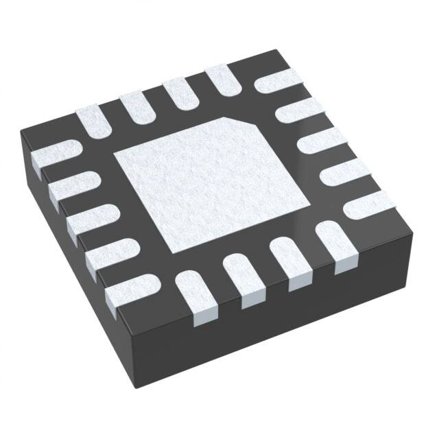
LTC3311
5V, 12.5A Synchronous Step-Down
Silent Switcher in 3mm x 3mm LQFN
FEATURES
DESCRIPTION
Pin Compatible with LTC3310/LTC3310S and LTC3311S
n Silent Switcher® Architecture:
n Ultralow EMI Emissions
n High Efficiency—4.5mΩ NMOS and 16mΩ PMOS
n Wide Bandwidth, Fast Transient Response
n Safely Tolerates Inductor Saturation in Overload
n V Range: 2.25V to 5.5V
IN
n V
OUT Range: 0.5V to VIN
n V
OUT Accuracy: ±1% with Remote Sense
n Peak Current Mode Control
n Minimum On-Time: 35ns
n Programmable Frequency to 5MHz
n Precision 400mV Enable Threshold, 1μA in Shutdown
n Output Soft-Start with Voltage Tracking
n Power Good Output
n Die Temperature Monitor
n Configurable for Paralleling Power Stages in Forced
Continuous Mode
n Thermally-Enhanced 3mm × 3mm LQFN Package
n AEC-Q100 Qualified for Automotive Applications
The LTC®3311 is a very small, low noise, monolithic
step-down DC/DC converter capable of providing up to
12.5A of output current from a 2.25V to 5.5V input supply.
The device employs Silent Switcher 1 architecture with
internal hot loop bypass capacitors to achieve both low
EMI and high efficiency at switching frequencies as high
as 5MHz. For systems with higher power requirements,
multi-phasing parallel converters is readily implemented.
n
The LTC3311 uses a constant frequency, peak current
mode control architecture for fast transient response. A
500mV reference allows for low voltage outputs. 100%
duty cycle operation delivers low drop out.
Other features include a power good signal when the
output is in regulation, precision enable threshold, output
overvoltage protection, thermal shutdown, a temperature
monitor, clock synchronization, mode selection and
output short circuit protection. The device is available in
a compact 18-lead 3mm x 3mm LQFN package.
All registered trademarks and trademarks are the property of their respective owners.
APPLICATIONS
Automotive/Industrial/Communications
Servers, Telecom Power Supplies
n Distributed DC Power Systems (POL)
n FPGA, ASIC, µP Core Supplies
n
n
TYPICAL APPLICATION
Efficiency
Efficiencyvs
vsLoad
LoadCurrent
Current
100
1.2V 12.5A Step-Down Converter
fSW = 2MHz Wurth HCM5030 74435030010
90
22µF
22µF
VIN
MODE/SYNC
PGOOD LTC3311
100nH
SW
6.8pF
FB
SSTT
0.1µF
AGND
ITH
10k
470pF
PGND
VIN
1μF
140k
100k
VOUT
1.2V
12.5A
47µF
×3
274k
3311 TA01a
3.2
70
2.8
60
2.4
50
2.0
40
30
1.2
VIN = 3.3V
VOUT = 1.2V
fOSC = 2MHz
10
0
1.6
POWER LOSS
20
RT
3.6
0
1
3
4
5
7 8
(A)
9
10 12 13
POWER LOSS (W)
EN
EFFICIENCY
80
EFFICIENCY (%)
VIN
3.0V to 5.5V
4.0
0.8
0.4
0
3311 TA01b
Rev. 0
Document Feedback
For more information www.analog.com
1
�LTC3311
ABSOLUTE MAXIMUM RATINGS
PIN CONFIGURATION
(Note 1)
VIN .............................................................. –0.3V to 6V
EN, SSTT.............. –0.3V to Lesser of (VIN + 0.3V) or 6V
MODE/SYNC......... –0.3V to Lesser of (VIN + 0.3V) or 6V
RT......................... –0.3V to Lesser of (VIN + 0.3V) or 6V
FB ......................... –0.3V to Lesser of (VIN + 0.3V) or 6V
PGOOD.......................................................... –0.3V to 6V
IPGOOD.......................................................................5mA
Operating Junction Temperature Range (Notes 2, 3)
LTC3311J.......................................... –40°C to +150°C
LTC3311H......................................... –40°C to +150°C
Storage Temperature............................ –65°C to +150°C
Maximum Reflow (Package Body) Temperature.... 260°C
FB
ITH
SSTT
RT
TOP VIEW
18
17
16
15
14 PGOOD
EN 1
13 MODE/SYNC
AGND 2
19
PGND
VIN 3
12 VIN
11 VIN
VIN 4
10 PGND
6
7
8
9
SW
SW
SW
SW
PGND 5
18-LEAD (3mm × 3mm) LQFN PACKAGE
θJA = 42°C/W, θJCbottom = 9°C/W, θJCtop = 62°C/W, θJB = 14°C/W
ΨJT = 1.25°C/W, θ VALUES DETERMINED PER JESD51-12
EXPOSED PAD (PIN 19) IS PGND, MUST BE SOLDERED TO PCB
ORDER INFORMATION
LEAD FREE – TRAY/REEL
AUTOMOTIVE PRODUCTS**
LTC3311JV#PBF
LTC3311JV#WPBF
LTC3311HV#PBF
LTC3311HV#WPBF
LTC3311JV#TRPBF
LTC3311JV#WTRPBF
LTC3311HV#TRPBF
LTC3311HV#WTRPBF
LTC3311JV#TRMPBF
LTC3311JV#WTRMPBF
LTC3311HV#TRMPBF
LTC3311HV#WTRMPBF
PART MARKING PACKAGE DESCRIPTION
LHMN
TEMPERATURE RANGE
18-Lead (3mm × 3mm) LQFN
(Laminate Package with QFN Footprint) –40°C to 150°C
Contact the factory for parts specified with wider operating temperature ranges. *The temperature grade is identified by a label on the shipping container.
Tape and reel specifications. Some packages are available in 500 unit reels through designated sales channels with #TRMPBF suffix.
**Versions of this part are available with controlled manufacturing to support the quality and reliability requirements of automotive applications. These
models are designated with a #W suffix. Only the automotive grade products shown are available for use in automotive applications. Contact your
local Analog Devices account representative for specific product ordering information and to obtain the specific Automotive Reliability reports for
these models.
2
Rev. 0
For more information www.analog.com
�LTC3311
ELECTRICAL CHARACTERISTICS
The l denotes the specifications which apply over the specified operating
temperature range, otherwise specifications are at TA = 25°C. (Notes 2, 3) VIN = 3.3V, VEN = VIN, MODE/SYNC = 0V, unless otherwise noted.
PARAMETER
CONDITIONS
MIN
TYP
MAX
UNITS
Input Supply
Operating Supply Voltage (VIN)
VIN Undervoltage Lockout
VIN Undervoltage Lockout Hysteresis
VIN Rising
VIN Quiescent Current
VIN Quiescent Current in Shutdown
(Note 4)
VEN = 0.1V
EN Threshold
EN Hysteresis
VEN Rising
EN Pin Leakage Current
VEN = 0.4V
l
2.25
l
2.0
l
0.375
5.5
V
2.1
150
2.2
V
mV
1.3
1
2.0
2
mA
μA
0.4
60
0.425
V
mV
±20
nA
Voltage Regulation
Regulated Feedback Voltage (VFB)
l
Feedback Voltage Line Regulation
2.5V ≤ VIN ≤ 5.0V
Feedback Pin Input Current
VFB = 0.5V
495
Error Amp Transconductance
Error Amp Sink/Source Current
500
505
mV
0.002
0.025
%/V
±20
nA
1
mS
±45
µA
Top Switch Current Limit
VOUT/VIN ≤ 0.2, Current Out of SW
l
15
18
21
Bottom Switch Current Limit (IVALLEYMAX)
Current Out of SW
l
12
14
16
Top Switch ON-Resistance
Bottom Switch ON-Resistance
SW Leakage Current
VEN = 0.1V
VITH to IPeak Current Gain
Minimum On-Time
l
Maximum Duty cycle
l
100
A
A
16
mΩ
4.5
mΩ
±100
nA
26
A/V
35
60
ns
%
Power Good/Soft-Start/Temp Monitor
PGOOD Rising Threshold
PGOOD Hysteresis
As a Percentage of the Regulated VOUT
l
l
97
0.5
98
1
99
1.5
%
%
Overvoltage Rising Threshold
Overvoltage Hysteresis
As a Percentage of the Regulated VOUT
l
l
105
1
110
2.5
115
3.5
%
%
PGOOD Leakage Current
VPGOOD = 5.5V
20
nA
PGOOD Pull Down Resistance
VPGOOD = 0.1V
20
Ω
12
PGOOD Delay
125
µs
PGOOD Input Threshold
PGOOD Input Hysteresis
Multi-Phase Mode, Rising
l
390
440
130
490
mV
mV
Soft-Start Charge Current
VSSTT = 0.5V
l
7
10
13
µA
Temp Monitor Slope
4
mV/°C
Oscillator
Switching Frequency Range
RT Programmable
l
0.5
Switching Frequency
RT = 274k
l
1.8
Synchronization Frequency Range
RT = VIN
l
0.5
Default Frequency
RT = VIN
l
1.8
l
l
1.2
SYNC Level High on MODE/SYNC
SYNC Level Low on MODE/SYNC
Minimum MODE/SYNC Pulse Width
40
2
2
5
MHz
2.2
MHz
2.25
MHz
2.2
MHz
0.4
V
V
ns
Rev. 0
For more information www.analog.com
3
�LTC3311
ELECTRICAL CHARACTERISTICS
The l denotes the specifications which apply over the specified operating
temperature range, otherwise specifications are at TA = 25°C. (Notes 2, 3) VIN = 3.3V, VEN = VIN, MODE/SYNC = 0V, unless otherwise noted.
PARAMETER
CONDITIONS
MIN
TYP
MODE/SYNC Input Resistance
MODE/SYNC No Clock Detect Time
MAX
UNITS
200
kΩ
20
µs
10
ns
MODE/SYNC Clock Out Rise/Fall Time
CMODE/SYNC = 50pF
MODE/SYNC Clock Low Output Voltage
IMODE/SYNC = 100µA
0.2
V
MODE/SYNC Clock High Output Voltage
IMODE/SYNC = 100µA
VIN – 0.2
V
50
%
MODE/SYNC Clock Out Duty Cycle
Note 3: The LTC3311 includes overtemperature protection which protects
the device during momentary overload conditions. Junction temperatures
will exceed 150°C when overtemperature protection is active. Continuous
operation above the specified maximum operating junction temperature
may impair device reliability.
Note 4: Supply current specification does not include switching currents.
Actual supply currents will be higher.
Note 1: Stresses beyond those listed under Absolute Maximum Ratings
may cause permanent damage to the device. Exposure to any Absolute
Maximum Rating condition for extended periods may affect device
reliability and lifetime.
Note 2: The LTC3311J/ LTC3311H are guaranteed to meet performance
specifications from –40°C to 150°C junction temperature.
TYPICAL PERFORMANCE CHARACTERISTICS
1.210
1.208
1.208
1.206
1.206
1.204
1.204
1.202
1.202
1.200
1.198
1.196
1.192
1.190
1.188
2.5
3
3.5
4
4.5
INPUT VOLTAGE (V)
5
1.198
1.194
1.190
1.188
0
2
4
10
60
50
40
30
100
90
0
0.001
12
100
fSW = 2MHz Wurth HCM5030 74435030010
90
70
70
70
30
VIN = 2.5V
VIN = 3.3V
VIN = 5V
10
0
0.001
0.01
0.1
ILOAD (A)
1
10 20
3311 G04
EFFICIENCY (%)
80
40
60
50
40
30
20
VIN = 2.5V
VIN = 3.3V
VIN = 5V
10
0
0.001
0.01
0.1
ILOAD (A)
0.1
ILOAD (A)
1
10 20
3311 G03
Efficiency, VOUT = 1.2V
Pulse
PulseSkip
SkipMode
ModeOperation
Operation
80
50
0.01
3311 G02
80
60
VIN = 2.5V
VIN = 3.3V
VIN = 5V
10
Efficiency, VOUT = 1.2V
Forced
ForcedContinuous
ContinuousOperation
Operation
EFFICIENCY (%)
EFFICIENCY (%)
8
ILOAD (A)
FSW = 2MHz, Wurth HCM5030 744350300055
20
4
6
70
20
VIN = 2.5V
VIN = 3.3V
VIN = 5V
1.192
5.5
FSW = 2MHz, Wurth HCM5030 744350300055
80
1.200
Efficiency, VOUT = 0.5V
Pulse Skip Mode Operation
90
100
90
3311 G01
100
Efficiency, VOUT = 0.5V
Forced Continuous Operation
1.196
ILOAD = 1A
LOAD = 3A
LOAD = 6A
LOAD = 9A
LOAD = 12A
1.194
VOUT Load Regulation
VInOUT
= 1.2V
VOUT
= 1.2V Application
EFFICIENCY (%)
1.212
1.210
VOUT (V)
VOUT (V)
1.212
VOUT Line Regulation
VInOUT
= 1.2V
VOUT
= 1.2V Application
VIN = 3.3V, TA = 25°C, unless otherwise noted.
1
10 20
3311 G05
fSW = 2MHz Wurth HCM5030 74435030010
60
50
40
30
20
VIN = 2.5V
VIN = 3.3V
VIN = 5V
10
0
0.001
0.01
0.1
ILOAD (A)
1
10 20
3311 G06
Rev. 0
For more information www.analog.com
�LTC3311
TYPICAL PERFORMANCE CHARACTERISTICS
Efficiency, VOUT = 1.8V
Forced Continuous Operation
100
100
Feedback Reference Voltage
505
fSW = 2MHz Wurth HCM5030 74435030010
504
80
80
503
70
70
60
50
40
30
50
40
30
20
VIN = 2.5V
VIN = 3.3V
VIN = 5V
10
0
0.001
0.01
0.1
1
0
0.001
10 20
ILOAD (A)
1
18
16
14
12
10
8
6
2.5
3.0 3.5 4.0 4.5
INPUT VOLTAGE (V)
50
497
Switch Leakage
10
5
2.3
VIN UVLO (V)
1.9
7
5
3
1
0
3311 G12
RISING
FALLING
RT = 274kHz
2.3
2.2
2.1
2.0
1.8
–50 –25
25 50 75 100 125 150
TEMPERATURE (°C)
Switching Frequency
1.9
25 50 75 100 125 150
TEMPERATURE (°C)
9
2.4
1.8
1.7
11
VIN
IN UVLO Threshold
2.2
2.0
VIN = 3.3V
PMOS
NMOS
–1
–50 –25
25 50 75 100 125 150
TEMPERATURE (°C)
DEFAULT FREQUENCY (MHz)
2.3
2.1
13
3311 G11
2.4
25 50 75 100 125 150
TEMPERATURE (°C)
3311 G09
15
15
0
0
3311 G08
PMOS
NMOS
20
Default
DefaultSwitching
SwitchingFrequency
Frequency
DEFAULT FREQUENCY (MHz)
498
VIN = 3.3V
0
–50 –25
5.5
2.4
0
499
495
–50 –25
10 20
3311 G10
1.6
–50 –25
500
496
4
2
2.0
501
Switch On Resistance
25
SWITCH ON–RESISTANCE (mΩ)
20
0.1
3311 G07
PMOS
NMOS
22
0.01
ILOAD (A)
Switch On Resistance vs VIN
24
VIN = 2.5V
VIN = 3.3V
VIN = 5V
10
502
SWITCH LEAKAGE CURRENT (μA)
20
60
FEEDBACK VOLTAGE (mV)
90
EFFICIENCY (%)
EFFICIENCY (%)
Efficiency, VOUT = 1.8V
Pulse Skip Mode Operation
fSW = 2MHz Wurth HCM5030 74435030010
90
RDS(ON) (mΩ)
VIN = 3.3V, TA = 25°C, unless otherwise noted.
2.2
2.1
2.0
1.9
1.8
1.7
0
25 50 75 100 125 150
TEMPERATURE (°C)
3311 G14
3311 G13
1.6
–50 –25
0
25 50 75 100 125 150
TEMPERATURE (°C)
3311 G15
Rev. 0
For more information www.analog.com
5
�LTC3311
TYPICAL PERFORMANCE CHARACTERISTICS
EN
ENPin
PinThresholds
Thresholds
EN RISING
380
370
360
EN FALLING
10.4
10.2
10.0
9.6
–50 –25
25 50 75 100 125 150
TEMPERATURE (°C)
0
IN
3.5
1.5
1.0
0.5
0
–50 –25
VIN = 2.25V
VIN = 3.3V
VIN = 5.5V
0
VIN
Shutdown Current
IN
14
1.5
–1.0
VFB RISING
VFB FALLING
0
8
6
1.0
4
2
0
0
–50 –25
25 50 75 100 125 150
TEMPERATURE (°C)
25 50 75 100 125 150
TEMPERATURE (°C)
3311 G22
PMOS ILIMIT
NMOS ILIMIT
0
25 50 75 100 125 150
TEMPERATURE (°C)
3311 G21
Minimum
Minimum On-Time
On-Time
10.0
80
9.5
70
9.0
MINIMUM ON-TIME (ns)
–1.5
0
–50 –25
10
3311 G20
PGOOD THRESHOLD OFFSET FROM VREF (%)
–2.0
–0.5
12
OV
OV PGOOD
PGOOD Threshold
Threshold
–2.5
600
16
2.0
UV PGOOD Threshold
500
Switch Current Limit
2.5
3311 G19
–3.0
200
300
400
SSTT VOLTAGE (mV)
18
0
–50 –25
25 50 75 100 125 150
TEMPERATURE (°C)
–3.5
100
20
0.5
–4.0
0
3311 G18
CURRENT (A)
VIN CURRENT (μA)
VIN CURRENT (mA)
0
3.0
2.0
PGOOD THRESHOLD OFFSET FROM VREF (%)
200
3311 G17
VIN Quiescent Current
6
300
25 50 75 100 125 150
TEMPERATURE (°C)
3311 G16
2.5
400
100
9.8
350
0
500
10.6
FB VOLTAGE (mV)
390
340
–50 –25
600
10.8
SOFT–START CURRENT (µA)
EN TRESHOLD (mV)
400
Soft-Start Tracking
Soft-Start Current
11.0
410
VIN = 3.3V, TA = 25°C, unless otherwise noted.
8.5
8.0
7.5
7.0
6.5
6.0
5.5
5.0
–50 –25
50
40
30
20
VIN = 5.5V
VIN = 3.3V
VIN = 2.25V
10
VFB RISING
VFB FALLING
0
60
25 50 75 100 125 150
TEMPERATURE (°C)
3311 G23
0
–50 –25
0
25 50 75 100 125 150
TEMPERATURE (°C)
3311 G24
Rev. 0
For more information www.analog.com
�LTC3311
TYPICAL PERFORMANCE CHARACTERISTICS
TA = 25°C, unless otherwise noted.
CISPR25 Conducted EMI Performance (CISPR25
Conducted
Conducted Emission
Emission Test
Test with
with Class
Class 55 Peak
Peak Limits)
Limits)
60
AMPLITUDE (dBµV/m)
50
40
30
20
10
0
CLASS 5 PEAK LIMIT
MEASURED EMISSIONS
AMBIENT NOISE
–10
–20
0
10
20
30
40
50
60
70
FREQUENCY (MHz)
80
90
Radiated EMI Performance (CISPR25 Radiated
Emissions Test with Class 5 Peak Limits)
60
HORIZONTAL POLARIZATION
50
50
40
40
AMPLITUDE (dBµV/m)
AMPLITUDE (dBµV/m)
60
30
20
10
0
CLASS 5 PEAK LIMIT
MEASURED EMISSIONS
AMBIENT NOISE
–10
–20
0
100
200
300
400
500
600
FREQUENCY (MHz)
700
800
900
1000
VERTICAL POLARIZATION
30
20
10
0
CLASS 5 PEAK LIMIT
MEASURED EMISSIONS
AMBIENT NOISE
–10
–20
0
100
3311 G26
DC3056A DEMO BOARD
(WITH EMI FILTER INSTALLED)
3.3V INPUT TO 1.2V OUTPUT AT 10A, fSW = 2MHz
110
3311 G25
DC3056A DEMO BOARD
(WITH EMI FILTER INSTALLED)
3.3V INPUT TO 1.2V OUTPUT AT 10A, fSW = 2MHz
Radiated EMI Performance (CISPR25 Radiated
Emissions
Emissions Test
Test with
with Class
Class 55 Peak
Peak Limits)
Limits)
100
200
300
400
500
600
FREQUENCY (MHz)
700
800
900
1000
3311 G27
DC3056A DEMO BOARD
(WITH EMI FILTER INSTALLED)
3.3V INPUT TO 1.2V OUTPUT AT 10A, fSW = 2MHz
Rev. 0
For more information www.analog.com
7
�LTC3311
PIN FUNCTIONS
EN (Pin 1): The EN pin has a precision enable threshold
with hysteresis. An external resistor divider, from VIN or
from another supply, programs the threshold below which
the LTC3311 will shut down. If the precision threshold is
not used, directly connect the pin to VIN. When the EN pin
is low, the LTC3311 enters a low current shutdown mode
where all internal circuitry is disabled.
AGND (Pin 2): The AGND pin is the output voltage remote
ground sense. Connect the AGND pin directly to the negative terminal of the output capacitor at the load and to the
feedback divider resistor.
VIN (Pins 3, 4, 11, 12): The VIN pins supply current to the
internal circuitry and topside power switch. All of the VIN
pins must be connected together with short, wide traces
and bypassed to PGND with low ESR capacitors located
as close as possible to the pins.
PGND (Pins 5, 10, 19): The PGND pins are the return
path of the internal bottom side power switch. Connect
the PGND pins together and to the exposed pad. Connect
the negative terminal of the input capacitors as close to
the PGND pins as possible. The PGND node is the main
thermal highway and should be connected to a large PCB
ground plane with many large vias.
SW (Pins 6–9): The SW pins are the switching outputs of
the internal power switches. Connect these pins together
to the inductor with short, wide traces.
MODE/SYNC (Pin 13): The MODE/SYNC pin facilitates
multiphase operation and synchronization to an external
clock. Depending on the mode of operation, the MODE/
SYNC pin either accepts an input clock pulse or outputs
a clock pulse at its operating frequency. (see Multiphase
Operation in Applications Information). The MODE/SYNC
pin also programs the mode of operation: pulse skip or
forced continuous.
8
PGOOD (Pin 14): The PGOOD pin is a power good pin and
is the open drain output of an internal comparator. The
PGOOD output is pulled low when VIN is above 2.25V and
the part is in shutdown. When connecting multiple phases
in parallel, connect the PGOOD pins together.
RT (Pin 15): The RT pin sets the oscillator frequency
with an external resistor to AGND or sets the phasing
for multiphase operation. (see Multiphase Operation in
Applications Information).
SSTT (Pin 16): Soft-Start, Track, Temperature Monitor.
An internal 10µA current into an external capacitor on the
soft-start pin programs the output voltage ramp rate during start-up. During the soft-start cycle, the FB pin voltage
will track the SSTT pin voltage. When the soft-start cycle
is complete, the tracking function is disabled, the internal
reference resumes control of the error amplifier and the
SSTT pin servos to a voltage representative of junction
temperature. For a clean recovery from an output short
circuit condition, the SSTT pin is pulled down to approximately 140mV above the VFB voltage and a new soft-start
cycle is initiated. During shutdown and fault conditions,
the SSTT pin is pulled to ground.
ITH (Pin 17): The ITH pin is the compensation node for
the output voltage regulation control loop. Compensation
components connected to this pin are referenced to AGND.
FB (Pin 18): The output voltage feedback pin is externally
connected to the output voltage via a resistive divider and
is internally connected to the inverting input of the error
amplifier. The LTC3311 regulates the FB pin to 500mV. A
phase lead capacitor connected between VFB and VOUT is
used to optimize the transient response.
Rev. 0
For more information www.analog.com
�LTC3311
BLOCK DIAGRAM
VIN
R1
EN
R2
+
–
0.4V
RT
RT
INTERNAL
REFERENCE
S
OSCILLATOR
Q
R
0.55V
0.5V
0.49V
VIN
SWITCH LOGIC
AND
ANTI-SHOOT THROUGH
CIN
L
SW
VIN
VOUT
COUT
SENSE+
+
–
MODE/SYNC
VIN
0.1µF
×2
PGND
SENSE–
SLOPE COMP
RC
+
RA
FB
0.5V
CFF
RB
AGND
CC
0.49V
–
+
0.55V
+
–
10µA
SSTT
CSS
+
–
ERROR
AMP
ITH
FAULT
+
–
VTEMP
PGOOD
FAULT
3311 BD
Rev. 0
For more information www.analog.com
9
�LTC3311
OPERATION
Voltage Regulation
Synchronizing the Oscillator to an External Clock
The LTC3311 is a monolithic, constant frequency, current
mode step-down DC/DC converter. An oscillator turns on
the internal top power switch at the beginning of each
clock cycle. Current in the inductor increases until the
top switch current comparator trips and turns off the top
power switch. The peak inductor current at which the top
switch turns off is controlled by the voltage on the ITH
node. The error amplifier servos the ITH node by comparing the voltage on the FB pin with an internal 500mV
reference. When the load current increases, it causes a
reduction in the feedback voltage relative to the reference
leading the error amplifier to raise the ITH voltage until the
average inductor current matches the new load current.
When the top power switch turns off, the synchronous
power switch turns on until the next clock cycle begins
or, in pulse-skipping mode, inductor current falls to zero.
If overload conditions result in excessive current flowing
through the bottom switch, the next clock cycle will be
delayed until switch current returns to a safe level.
The LTC3311’s internal oscillator is synchronized through
an internal PLL circuit to an external frequency by applying a square wave clock signal to the MODE/SYNC pin.
The output voltage is resistively divided externally to create a feedback voltage for the regulator. In high current
operation, a ground offset may be present between the
LTC3311 local ground and ground at the load. To overcome this offset, AGND should have a Kelvin connection to the load ground, and the lowest potential node of
the resistor divider should be connected to AGND. The
internal error amplifier senses the difference between
this feedback voltage and a 0.5V AGND referenced voltage. This scheme overcomes any ground offsets between
local ground and remote output ground, resulting in a
more accurate output voltage. The LTC3311 allows for
remote output ground deviations as much as ±100mV
with respect to local ground.
Mode Selection
If the EN pin is low, the LTC3311 is shut down and in a
low quiescent current state. When the EN pin is above its
threshold, the switching regulator will be enabled.
10
During synchronization, the top power switch turn-on is
locked to the rising edge of the external frequency source.
While synchronizing, the switcher operates in forced continuous mode. The slope compensation is automatically
adapted to the external clock frequency.
After detecting an external clock on the first rising edge
of the MODE/SYNC pin, the internal PLL gradually adjusts
its operating frequency to match the frequency and phase
of the signal on the MODE/SYNC pin. When the external
clock is removed, the LTC3311 detects the absence of
the external clock within approximately 20µs. During this
time, the PLL will continue to provide clock cycles. Once
the external clock removal has been detected, the oscillator gradually adjusts its operating frequency back to the
default frequency.
The MODE/SYNC pin either synchronizes the switching frequency to an external clock, is a clock output, or
sets the PWM mode. The PWM modes of operation are
either pulse skip or forced continuous. See Table 6 in
the Applications Information section. In pulse skip mode,
switching cycles are skipped at light loads to regulate the
output voltage. During forced continuous mode, the top
switch turns on every cycle and light load regulation is
achieved by allowing negative inductor current.
Output Power Good
Comparators monitoring the FB pin voltage pull the
PGOOD pin low if the output voltage varies from the
nominal set point or if a fault condition is present. The
comparator includes voltage hysteresis. A time delay to
report PGOOD is used to filter short duration output voltage transients.
Rev. 0
For more information www.analog.com
�LTC3311
OPERATION
Soft-Start/Tracking/Temperature Monitor
Output Short-Circuit Protection and Recovery
The soft-start tracking function facilitates supply sequencing, limits VIN inrush current and reduces start-up output
overshoot. When soft-starting is completed, the SSTT pin
parks itself at a voltage representative of the LTC3311
die junction temperature. The SSTT capacitor is reset
during shutdown, VIN UVLO and thermal shutdown. See
Application section.
The peak inductor current level, at which the current comparator shuts off the top power switch, is controlled by the
voltage on the ITH pin. If the output current increases, the
error amplifier raises the ITH pin voltage until the average
inductor current matches the load current. The LTC3311
clamps the maximum ITH pin voltage, thereby limiting the
peak inductor current.
Dropout Operation
When the output is shorted to ground, the inductor current decays very slowly during a single switching cycle
because the voltage across the inductor is low. To keep
the inductor current in control, a secondary limit is
imposed on the valley of the inductor current. If the inductor current measured through the bottom power switch
is greater than the IVALLEY(MAX) the top power switch will
be held off. Subsequent switching cycles will be skipped
until the inductor current is reduced below IVALLEY(MAX).
As the input supply voltage approaches the output voltage, the duty cycle increases. Further reduction of the
supply voltage forces the main switch to remain on for
more than one cycle, eventually reaching 100% duty
cycle. The output voltage will then be determined by the
input voltage minus the DC voltage drop across the internal main P-channel MOSFET and the inductor.
In many designs when the input voltage approaches the
output voltage, the amplitude of the output ripple voltage increases from its normally low value. To avoid any
increase in output ripple voltage under these conditions,
it is recommended to utilize a resistor divider on the EN
input and limit the VIN turn-on and turn-off thresholds to
where the output ripple voltage is acceptable for the given
application (typically 500mV above VOUT).
Recovery from an output short circuit goes through a
soft-start cycle. When VOUT goes below regulation, as
defined by the PGOOD threshold, the SSTT voltage is
pulled to a voltage just above the FB voltage. Because
the SSTT pin is pulled low, a soft-start cycle is initiated
once the output short is removed.
Low Supply Operation
The LTC3311 is designed to operate down to an input
supply voltage of 2.25V. An important thermal design
consideration is that the RDS(ON) of the power switches
increase at low VIN. Calculate the worst case LTC3311
power dissipation and die junction temperature at the lowest input voltages.
Rev. 0
For more information www.analog.com
11
�LTC3311
APPLICATIONS INFORMATION
Refer to the Block Diagram for reference.
switching frequency (fSW(MAX)) for a given application
can be calculated using Equation 2.
FB Resistor Network
The output voltage is programmed with a resistor divider
between the output and the FB pin. Choose the resistor
values according to Equation 1.
⎛ V
⎞
RA = RB ⎜ OUT – 1⎟ (1)
⎝ 500mV ⎠
as shown in Figure 1:
VOUT
BUCK
SWITCHING FB
REGULATOR
RA
RB
CFF
+
COUT
(OPTIONAL)
3311 F01
fSW(MAX ) =
tON(MIN) VIN(MAX ) – VSW( TOP ) + VSW(BOT )
)
(2)
where VIN(MAX) is the maximum input voltage, VOUT is the
output voltage, VSW(TOP) and VSW(BOT) are the internal
switch drops and tON(MIN) is the minimum top switch ontime. Equation 2 shows that a slower switching frequency
is necessary to accommodate a high VIN/VOUT ratio.
The LTC3311 is capable of a maximum duty cycle of
100%, therefore, the VIN-to-VOUT dropout is limited by
the RDS(ON) of the top switch, the inductor DCR and the
load current.
Setting the Switching Frequency
Figure 1. Feedback Resistor Network
Reference designators refer to the Block Diagram. 1%
resistors are recommended to maintain output voltage
accuracy. When optimizing the control loop for high bandwidth and optimal transient response add a phase-lead
capacitor connected from VOUT to FB.
Operating Frequency Selection and Trade-Offs
Selection of the operating frequency is a trade-off between
efficiency, component size, transient response and input
voltage range.
The advantage of high frequency operation is that smaller
inductor and capacitor values may be used. Higher
switching frequencies allow for higher control loop
bandwidth and, therefore, faster transient response. The
disadvantages of higher switching frequencies are lower
efficiency, because of increased switching losses, and a
smaller input voltage range, because of minimum switch
on-time limitations.
The LTC3311 uses a constant frequency PWM architecture. There are three methods to set the switching frequency. The first method is with a resistor (RT) tied from
the RT pin to ground. The frequency can be programmed
to switch from 500kHz to 5MHz. Table 1 shows the necessary RT value for a desired switching frequency.
The RT resistor required for a desired switching frequency
is calculated using Equation 3.
(3)
(–1.08)
RT = 568 • fSW
where RT is in kΩ and fSW is the desired switching frequency in MHz.
Table 1. SW Frequency vs RT Value
fSW (MHz)
RT (kΩ)
0.5
1210
1
549
2
274
2.2
243
3
178
4
130
5
100
Although the maximum programmable switching frequency is 5MHz, the minimum on-time of the LTC3311
imposes a minimum operating duty cycle. The highest
12
(
VOUT + VSW(BOT )
Rev. 0
For more information www.analog.com
�LTC3311
APPLICATIONS INFORMATION
The second method to set the LTC3311 switching frequency is by synchronizing the internal PLL circuit to an
external frequency applied to the MODE/SYNC pin. The
synchronization frequency range is 0.5MHz to 2.25MHz.
The internal PLL starts up at the 2MHz default frequency.
After detecting an external clock on the first rising edge
of the MODE/SYNC pin, the internal PLL gradually adjusts
its operating frequency to match the frequency and phase
of the MODE/SYNC signal.
The LTC3311 detects when the external clock is removed
and will gradually adjust its operating frequency to the
2MHz default frequency. The LTC3311 operates in forced
continuous mode when synchronized to an external clock.
The third method of setting the LTC3311 switching frequency is to use the internal nominal 2MHz default clock.
See Table 4 for pin configuration.
Inductor Selection and Maximum Output Current
Considerations in choosing an inductor are inductance,
RMS current rating, saturation current rating, DCR and
core loss.
A good first choice for the inductor value is given by
Equation 4 and Equation 5.
L≈
L≈
⎛
⎞
V
VOUT
V
• ⎜ 1− OUT ⎟ for OUT ≤ 0.5 (4)
4A • fSW ⎝ VIN(MAX) ⎠
VIN(MAX)
0.25• VIN(MAX)
4A • fSW
for
VOUT
VIN(MAX)
> 0.5 (5)
where fSW is the switching frequency in MHz, VIN is the
input voltage and L is the inductor value in μH.
To avoid overheating of the inductor, choose an inductor with
an RMS current rating that is greater than the maximum
expected output load of the application. Overload and short
circuit conditions may need to be taken into consideration.
In addition, the saturation current (ISAT) rating of the
inductor must be higher than the load current plus 1/2 of
the inductor ripple current (Equation 6).
1
I SAT ≥ILOAD(MAX ) + ∆IL
2
where ILOAD(MAX) is the maximum output load current for
a given application and ΔIL is the inductor ripple current
calculated using Equation 7.
∆IL =
⎞
VOUT ⎛
V
• ⎜⎜1– OUT ⎟⎟ (7)
L • fSW ⎝ VIN(MAX) ⎠
where VIN(MAX) is the maximum application input voltage.
To keep the efficiency high, choose an inductor with the
lowest series resistance (DCR). The core material should
be intended for high frequency applications.
The LTC3311 limits the peak switch current in order to
protect the switches and the system from overload faults.
The inductor value must then be sufficiently large to supply the desired maximum output current, IOUT(MAX), which
is a function of the switch current limit, ILIM, and the ripple
current (Equation 8).
IOUT(MAX ) = ILIM – ∆IL (8)
Therefore, the maximum output current that the LTC3311
will deliver depends on the switch current limit, the inductor value, and the input and output voltages. The inductor
value may have to be increased if the inductor ripple current does not allow sufficient maximum output current
(IOUT(MAX)) given the switching frequency, and maximum
input voltage used in the desired application.
Table 2. Inductor Manufacturers
VENDOR
URL
Coilcraft
www.coilcraft.com
Sumida
www.sumida.com
Toko
www.toko.com
Wurth Elektronik
www.we-online.com
Vishay
www.vishay.com
XFMRS
www.xfmrs.com
Input Capacitors
Bypass the input of the LTC3311 with at least two bulk
storage ceramic capacitors close to the part, one on each
side from VIN to PGND. These capacitors should be 0603
or 0805 in size. See layout section for more detail. X7R or
(6)
Rev. 0
For more information www.analog.com
13
�LTC3311
APPLICATIONS INFORMATION
X5R capacitors are recommended for best performance
across temperature and input voltage variations. Note that
larger input capacitance is required when a lower switching frequency is used. For high frequency applications,
adding two small capacitors close to the part is recommended. If the input power source has high impedance, or
there is significant inductance due to long wires or cables,
additional bulk capacitance may be necessary. This can
be provided with a low performance electrolytic capacitor.
X5R or X7R type capacitors will provide low output ripple
and good transient response. Transient performance is
improved with a higher value output capacitor and the
addition of a feedforward capacitor placed between
VOUT and FB. Increasing the output capacitance will also
decrease the output voltage ripple. A lower value of output
capacitor saves space and cost but transient performance
will suffer and may cause loop instability. See the Typical
Applications for suggested capacitor values.
A ceramic input capacitor combined with trace or cable
inductance forms a high quality (under damped) tank
circuit. If the LTC3311 circuit is plugged into a live supply, the input voltage can ring to twice its nominal value,
possibly exceeding the LTC3311’s voltage rating. This
situation is easily avoided (see Analog Devices Application
Note 88).
Multiphase Operation
Table 3. Ceramic Capacitor Manufacturers
VENDOR
URL
AVX
www.avxcorp.com
Murata
www.murata.com
TDK
www.tdk.com
Taiyo Yuden
www.t-yuden.com
Samsung
www.samsungsem.com
The LTC3311 is easily configurable for multiphase operation. See Table 4.
Connecting the RT pin, of the master phase, to a resistor to AGND programs the frequency and configures the
MODE/SYNC pin to become clock output used to drive
the MODE/SYNC pin of the slave phase(s).
Connecting the RT pin of the master phase to VIN configures the MODE/SYNC pin to become an input capable
of accepting an external clock. The switching frequency
defaults to the nominal 2MHz internal frequency when
the external clock is unavailable, such as during start-up.
Output Capacitor and Output Ripple
The output capacitor has two essential functions. Along
with the inductor, it filters the square wave, generated
by the LTC3311, to produce the DC output. In this role
it determines the output ripple, thus, low impedance at
the switching frequency is important. The second function is to store energy in order to satisfy transient loads
and stabilize the LTC3311’s control loop. Ceramic capacitors have very low equivalent series resistance (ESR) and
provide the best ripple performance. For good starting
values, see the Typical Applications section.
Connecting the FB pin to VIN configures a phase as a
slave. The MODE/SYNC becomes an input and the voltage
control loop is disabled. The slave phase current control
loop is still active and the peak current is controlled via the
shared ITH node. Careful consideration should be taken
when routing the ITH node between phases. Routing the
ITH and AGND nodes together is recommended to create
a low inductance path. See the Multi-Phase Demo Board
PCB layout as an example.
Connecting the PGOOD pins together and adding an external pull-up resistor allows the master phase to communicate with the slave phases on when start-up has been
completed.
Table 4. LTC3311 Multiphase Configuration
14
Master/Slave
RT Pin
FB Pin
MODE/SYNC Pin
Switching Frequency (fSW)
Master
VIN
VOUT Divider
Clock Input
External Clock/2MHz Default
Master
Resistor to AGND
VOUT Divider
Clock Output
RT programmed
Slave
VIN Divider
VIN
Clock Input
External Clock
Rev. 0
For more information www.analog.com
�LTC3311
APPLICATIONS INFORMATION
The phasing of a slave phase relative to the master phase
is programmed with a resistor divider on the RT pin. Use
of 1% resistors is recommended. See Table 5 for more
information.
Table 5. LTC3311 Programming Slave Phase Angle
SYNC
Phase
Angle
R3
Ratio
R4
Ratio
R3
Example
R4
Example
0°
0Ω
NA
0Ω
NA
90°
3•R
R
301k
100k
120°
7•R
5•R
243k
174k
180°
NA
0Ω
NA
0Ω
240°
5•R
7•R
174k
243k
270°
R
3•R
100k
300k
When configured for master/slave operation, the slave
phases operate in forced continuous modes.
RT Pin
Connection
MODE/SYNC
Pin Connection
MODE of
Operation
Switching
Frequency
VIN
Clock Input
Forced
Continuous
External Clock
VIN
AGND
Forced
Continuous
2MHz Default
VIN
VIN
Pulse Skip
2MHz Default
Resistor to AGND
Clock Output
Forced
Continuous
RT Programmed
Synchronization
To synchronize the LTC3311 oscillator to an external frequency, configure the MODE/SYNC pin as an input by
connecting the RT pin to VIN. Drive the MODE/SYNC pin
with a square wave in the frequency range of 500 kHz to
2.25MHz range, an amplitude greater than 1.2V and less
than 0.4V with a pulse width greater than 40ns.
The LTC3311 phase locked loop (PLL) will synchronize
the internal oscillator to the clock applied to the MODE/
SYNC pin. At start up, before the LTC3311 recognizes
the external clock applied to MODE/SYNC, the LTC3311
will switch at its default frequency of 2MHz. Once the
externally applied clock is recognized, the switching
frequency will gradually transition from the default frequency to the applied frequency. If the external clock is
removed, the LTC3311 will slowly transition back to the
default frequency.
VIN
FB
LTC3311
Table 6. LTC3311 Single Phase Configuration
R3
RT
R4
3311 F02
AGND
Figure 2. Phase Programming
MODE of Operation
For most configurations, the LTC3311 operates in forced
continuous mode. While in forced continuous mode, regulation at low currents is achieved by allowing negative
inductor current. Switching cycles are not skipped.
The LTC3311 operates in pulse skip mode when both RT
and MODE/SYNC pins are connected to VIN. In this mode,
the switching frequency is set with the nominal 2MHz
internal clock. While in pulse skip mode negative current
is disallowed and regulation at low currents is achieved
by skipping switching cycles.
The LTC3311 operates in forced continuous mode during
synchronization. An internal 200kΩ resistor on MODE/SYNC
pin to AGND allows the MODE/SYNC pin to be left floating.
Transient Response and Loop Compensation
When determining the compensation components, CFF,
RC, and CC, control loop stability and transient response
are the two main considerations.
The LTC3311 has been designed to operate at a high bandwidth for fast transient response capability. Operating at
a high loop bandwidth reduces the output capacitance
required to meet transient response requirements.
Applying a load transient and monitoring the response of
the system or using a network analyzer to measure the
actual loop response are two ways to verify and optimize
Rev. 0
For more information www.analog.com
15
�LTC3311
APPLICATIONS INFORMATION
the control loop stability. LTpowerCAD® is a useful tool to
help optimize the compensation components.
When using the load transient response method to stabilize the control loop, apply an output current pulse of
20% to 100% of full load current having a rise time of
1µs. This will produce a transient on the output voltage
and ITH pin waveforms.
Switching regulators take multiple cycles to respond to
a step in load current. When a load step occurs, VOUT is
immediately perturbed, generating a feedback error signal
used by the regulator to return VOUT to its steady-state
value.
During this recovery time, monitor VOUT for overshoot
or ringing that would indicate a stability problem. The
initial output voltage step may not be within the bandwidth of the feedback loop, so the standard second order
overshoot/DC ratio cannot be used to determine phase
margin. The gain of the loop increases with the RC and the
bandwidth of the loop increases with decreasing CC. If RC
is increased by the same factor that CC is decreased, the
zero frequency will be kept the same, thereby keeping the
phase the same in the most critical frequency range of the
feedback loop. In addition, adding a feed forward capacitor, CFF, improves the high frequency response. Capacitor
CFF provides phase lead by creating a high frequency zero
with RA to improve the phase margin. The compensation
components of the typical application circuits are a good
starting point for component values.
The output voltage settling behavior is related to the stability of the closed-loop system. For a detailed explanation
of optimizing the compensation components, including
a review of control loop theory, refer to Analog Devices
Application Note 76.
Output Overvoltage Protection
During an output overvoltage event, when the FB pin voltage is greater than 110% of nominal, the LTC3311 top
power switch will be turned off. If the output remains out
of regulation for more than 100µs, the PGOOD pin will
be pulled low.
An output overvoltage event should not happen under
normal operating conditions.
16
Output Voltage Sensing
The LTC3311 AGND pin is the ground reference for the
internal analog circuitry, including the bandgap voltage
reference. To achieve good load regulation, connect the
AGND pin to the negative terminal of the output capacitor (COUT) at the load. A drop in the high current power
ground return path will be compensated. All of the signal
components, such as the FB resistor dividers and softstart capacitor, should be referenced to the AGND node.
The AGND node carries very little current and, therefore,
can be a minimal size trace. See the example PCB Layout
for more information.
Enable Threshold Programming
The LTC3311 has a precision threshold enable pin
to enable or disable switching. When forced low, the
LTC3311 enters a low current shutdown mode.
The rising threshold of the EN comparator is 400mV, with
60mV of hysteresis. Connect the EN pin to VIN if the shutdown feature is not used. Adding a resistor divider from
VIN to EN programs the LTC3311 to regulate the output
only when VIN is above a desired voltage (see the Block
Diagram). Typically, this threshold, VIN(EN), is used in situations where the input supply is current limited or has a
relatively high source resistance. A switching regulator
draws constant power from the source, so source current
increases as source voltage drops. This looks like a negative resistance load to the source and can cause the source
to current limit or latch low under low source voltage conditions. The VIN(EN) threshold prevents the regulator from
operating at source voltages where problems may occur.
This threshold can be adjusted by setting the values R1
and R2 such that they satisfy Equation 9.
⎛ R1 ⎞
VIN(EN) = ⎜ + 1⎟ • 400mV (9)
⎝ R2 ⎠
where the LTC3311 will remain off until VIN is above
VIN(EN). Due to the comparator’s hysteresis, switching
will not stop until the input falls slightly below VIN(EN).
Alternatively, a resistor divider from an output of another
regulator to the enable pin of the LTC3311 provides eventbased power-up sequencing, enabling the LTC3311 when
Rev. 0
For more information www.analog.com
�LTC3311
APPLICATIONS INFORMATION
the output of the other regulator reaches a predetermined
level.
The following procedure is used for a more accurate measurement of the junction temperature:
Output Voltage Tracking and Soft-Start
1. Measure the ambient temperature TA.
The LTC3311 allows the user to program its output voltage ramp rate by means of the SSTT pin.
An internal 10μA pulls up the SSTT pin. Putting an external
capacitor on SSTT enables soft-starting the output to prevent current surge on the input supply and output voltage
overshoot. During the soft-start ramp, the output voltage will proportionally track the SSTT pin voltage. When
the soft-start is complete, the pin will servo to a voltage
proportional to the LTC3311 junction temperature. See
Figure 3 showing the SSTT pin operating range.
The soft-start time is calculated using Equation 10.
t SS = CSS •
500mV
(10)
10µA
For output tracking applications, SSTT can be externally
driven by another voltage source. From 0V to 0.5V, the
SSTT voltage will override the internal 0.5V reference
input to the error amplifier, thus regulating the FB pin
voltage to that of SSTT pin. When SSTT is above 0.5V,
tracking is disabled and the feedback voltage will regulate
to the internal reference voltage
An active pull-down circuit is connected to the SSTT pin
to discharge the external soft-start capacitor in the case
of fault conditions. The ramp will restart when the fault is
cleared. Fault conditions that clear the soft-start capacitor
are the EN/UV pin transitioning low, VIN voltage falling too
low or thermal shutdown.
Temperature Monitor
Once the soft-start cycle has completed and the output
power good flag thrown, the SSTT pin reports the die
junction temperature. The LTC3311 regulates the SSTT
pin to a voltage proportional to the junction temperature.
While reporting the temperature, the SSTT voltage is not
valid below 1V. The junction temperature is calculated
with Equation 11.
TJ (°C) =
VSSTT
– 273
4mV
(11)
2. Measure the SSTT voltage while in pulse skip mode
with the VOUT pulled up slightly higher than the
regulated VOUT.
3. Calculate the slope of the temperature sensing circuit
with Equation 12.
Slope (mV / °C) =
VSSTT
TA + 273
(12)
4. Calculate the junction temperature with the new calibrated slope.
When the output voltage goes out of regulation and the
power good pin is pulled low, the soft-start pin no longer
reports the temperature.
150
125
DIE TEMP 100
(°C) 75
SSTT PIN VOLTAGE
OPERATING RANGE
TEMP
MONITOR
~4mV/°C
50
25
0.6
0.5
0.4
FB
0.3
(V)
0.2
0.1
0
SOFT-START
AND TRACKING
0 0.1 0.2 0.3 0.4 0.5 0.6 1.2 1.3 1.4 1.5 1.6 1.7
SSTT (V)
3311 F03
Figure 3. Soft-Start and Temperature Monitor Operation
Output Power Good
When the LTC3311’s output voltage is within the –2/+10%
window of the nominal regulation voltage the output is
considered good and the open-drain PGOOD pin goes
high impedance and is typically pulled high with an external resistor. Otherwise, the internal pull-down device will
pull the PGOOD pin low. To prevent glitching both the
upper and lower thresholds, include 1% of hysteresis as
well as a built in time delay, typically 100µs. The PGOOD
Rev. 0
For more information www.analog.com
17
�LTC3311
APPLICATIONS INFORMATION
pin is also actively pulled low during fault conditions: EN
pin is low, VIN is too low or in thermal shutdown.
For multiphase applications the PGOOD pin is used for
communication between the master and slave phases.
Connect the PGOOD pins together and pull-up to VIN or
VOUT with an external resistor.
Output Short Circuit Protection and Recovery
The peak inductor current at which the current comparator shuts off the top power switch is controlled by the
voltage on the ITH pin. If the output current increases,
the error amplifier raises the ITH pin voltage until the
average inductor current matches the new load current.
In normal operation, the LTC3311 clamps the maximum
ITH pin voltage.
The LTC3311 does not have any internal bypass capacitors
and hence requires three additional 0201 external capacitors (CIN5, CIN6, and CIN7), as shown in Figure 4. Place
these capacitors as close as possible to the IC.
To avoid noise coupling into FB, the resistor divider
should be placed near the FB and AGND pins and physically close to the LTC3311. The remote output and ground
traces should be routed together as a differential pair to
the remote output. These traces should be terminated as
close as physically possible to the remote output point
that is to be accurately regulated through remote differential sensing.
See Figure 4 for a recommended PCB layout.
When the output is shorted to ground, the inductor current decays very slowly during the switch off time because
of the low voltage across the inductor. To keep the current
in control, a secondary limit is also imposed on the valley
inductor current. If the inductor current measured through
the bottom power switch increases beyond IVALLEY(MAX),
the top power switch will be held off and switching cycles
will be skipped until the inductor current is reduced.
Recovery from a short circuit can be abrupt and because
the output is shorted and below regulation the regulator
is requesting the maximum current to charge the output.
When the short circuit condition is removed, the inductor current could cause an extreme voltage overshoot in
the output. The LTC3311 addresses this potential issue
by regulating the SSTT voltage just above the FB voltage anytime the output is out of regulation. Therefore,
a recovery from an output short circuit goes through a
soft-start cycle. The output ramp is controlled and the
overshoot is minimized.
The LTC3311 is specifically designed to minimize EMI/
EMC emissions and also to maximize efficiency when
switching at high frequencies. For optimal performance,
the LTC3311 requires the use of multiple VIN bypass
capacitors.
18
CC1
CSS
CFF
RT
RA
CC2
RB
CIN7 1
RC
14
18
15
CIN6
19
5
CIN1
6
9
10
CIN2
CIN5
GND
GND
COUT1
TO VOUT & GND
REMOTE SENSE
Low EMI PCB Layout
GROUND PLANE ON LAYER 2
VIN
L
COUT2
VOUT
3310 F04
Figure 4. Recommended PCB Layout for the LTC3311
Rev. 0
For more information www.analog.com
�LTC3311
APPLICATIONS INFORMATION
High Temperature Considerations
Large, switched currents flow in the LTC3311 VIN, SW and
PGND pins and the input capacitors. The loops formed
by the input capacitors should be as small as possible by
placing the capacitors adjacent to the VIN and PGND pins.
Place the input capacitors, inductor and output capacitors on the same layer of the circuit board. Place a local,
unbroken ground plane under the application circuit on
the layer closest to the surface layer.
For higher ambient temperatures, care should be taken
in the layout of the PCB to ensure good heat sinking of
the LTC3311. The PGND pins and the exposed pad on the
bottom of the package should be soldered to a ground
plane. This ground should be tied to large copper layers
below with many thermal vias; these layers will spread
heat dissipated by the LTC3311. Placing additional vias
can reduce thermal resistance further. The maximum load
current should be derated as the ambient temperature
approaches the maximum junction rating. Power dissipation within the LTC3311 can be estimated by calculating the total power loss from an efficiency measurement
and subtracting the inductor loss. The die temperature is
monitored with the SSTT pin.
The SW node should be as short as possible. Finally,
keep the FB and RT nodes small and away from the noisy
SW node.
TYPICAL APPLICATIONS
Dual Phase 5V to 3.3V, 25A, Forced Continuous Mode
VIN
4.5V TO 5.5V
1µF
22µF
0.01µF
1M
0.01µF
VIN
EN
PGOOD
100k
SW
100k
4.7pF
4.99k
274k
FB
RT
AGND PGND
PGOOD
VOUT
3.3V
25A
200nH
LTC3311
MODE/SYNC
ITH
SSTT
22µF
22µF
x3
48.7k
274k
0.1µF
470pF
VIN
1µF
22µF
0.01µF
VIN
EN
PGOOD
MODE/SYNC
NC
22µF
0.01µF
SSTI
ITH
LTC3311
SW
FB
200nH
PGOOD
22µF
×2
VIN
AGND PGND RT
180°
3311 TA02
L = COILCRAFT, XEL4030-201ME
Rev. 0
For more information www.analog.com
19
�LTC3311
TYPICAL APPLICATIONS
Three Phase, 0.6V, 37.5A, Forced Continuous Mode
VIN
3.0V TO 4.5V
1µF
22µF
0.01µF
VIN
EN
PGOOD
MODE/SYNC
0.01µF
100k
PGOOD
70nH
SW
10pF
LTC3311
ITH
5.49k
22µF
86.6k
47µF
×3
FB
SSTT
1500pF
VOUT
0.6V
37.5A
RT
AGND PGND
432k
274K
0.1µF
VIN
1µF
22µF
0.01µF
VIN
EN
MODE/SYNC
NC
SSTT
SW
LTC3311
ITH
22µF
0.01µF
PGOOD
70nH
PGOOD
VIN
47µF
×2
FB
243k
120°
AGND PGND RT
174k
VIN
1µF
22µF
0.01µF
VIN
EN
PGOOD
MODE/SYNC
NC
SSTT
ITH
LTC3311
SW
22µF
0.01µF
PGOOD
70nH
VIN
47µF
×2
FB
174k
240°
AGND PGND RT
243k
3311 TA03
L = COILCRAFT XEL3520-700MEB
20
Rev. 0
For more information www.analog.com
�LTC3311
TYPICAL APPLICATIONS
Four Phase, 2MHz, 1.2V, 50A, Forced Continuous Mode
VIN
3.0V TO 5.5V
1µF
22µF
0.01µF
VIN
EN
PGOOD
MODE/SYNC
SW
6.8pF
LTC3311
ITH
3.32k
SSTT
470pF
0.01µF
100k
PGOOD
100nH
FB
RT
AGND PGND
140k
22µF
VOUT
1.2V
50A
22µF
x3
100k
274k
0.1µF
VIN
1µF
22µF
0.01µF
VIN
EN
0.01µF
PGOOD
MODE/SYNC
NC
SSTT
SW
LTC3311
ITH
22µF
PGOOD
100nH
VIN
22µF
x2
FB
301k
90°
AGND PGND RT
100k
VIN
1µF
22µF
0.01µF
VIN
EN
PGOOD
MODE/SYNC
NC
SSTT
SW
LTC3311
ITH
FB
0.01µF
PGOOD
100nH
22µF
22µF
x2
VIN
180°
AGND PGND RT
VIN
1µF
22µF
0.01µF
VIN
EN
PGOOD
MODE/SYNC
NC
SSTT
ITH
LTC3311
SW
0.01µF
PGOOD
100nH
VIN
22µF
22µF
x2
FB
100k
270°
AGND PGND RT
301k
3311 TA04
L = COILCRAFT, XEL4030-101ME
Rev. 0
For more information www.analog.com
21
�LTC3311
TYPICAL APPLICATIONS
Four Phase, 2MHz, 1.2V, 50A Driven with External Clock, Forced Continuous Mode
VIN
3.0V TO 5.5V
1µF
22µF
0.01µF
0.01µF
VIN
EN
PGOOD
MODE/SYNC
EXTERNAL
CLOCK
SW
6.8pF
LTC3311
ITH
3.32k
SSTT
470pF
22µF
PGOOD
100nH
FB
RT
AGND PGND
VOUT
1.2V
50A
140k
22µF
x3
VIN
100k
0.1µF
VIN
1µF
22µF
0.01µF
VIN
EN
PGOOD
MODE/SYNC
NC
SSTT
SW
LTC3311
ITH
0.01µF
PGOOD
100nH
VIN
22µF
22µF
x2
FB
301k
90°
AGND PGND RT
100k
VIN
1µF
22µF
0.01µF
VIN
EN
PGOOD
MODE/SYNC
NC
SSTT
SW
LTC3311
ITH
0.01µF
PGOOD
100nH
22µF
x2
VIN
FB
22µF
180°
AGND PGND RT
VIN
1µF
22µF
0.01µF
VIN
EN
PGOOD
MODE/SYNC
NC
SSTT
ITH
LTC3311
SW
0.01µF
PGOOD
100nH
VIN
22µF
22µF
x2
FB
100k
270°
AGND PGND RT
301k
3311 TA05
L = COILCRAFT, XEL4030-101ME
22
Rev. 0
For more information www.analog.com
�LTC3311
TYPICAL APPLICATIONS
5MHz, 1V, 12.5A, Forced Continuous Mode
VIN
3.0V TO 3.6V
22µF
0.1µF
649k
EN
0.1µF
VIN
22µF
PGOOD
100k
55nH
MODE/SYNC
0.1µF
SSTT
VOUT
1V
12.5A
SW
10pF
LTC3311
FB
100k
VIN
1μF
AGND
22µF
×3
100k
ITH
4.12k
PGND
RT
100k
680pF
WURTH 744340300055
3311 TA06
2MHz, 3.3V, 12.5A, Pulse Skip Mode
VIN
4.5V TO 5.5V
22µF
0.1µF
0.1µF
1M
EN
VIN
PGOOD
100k
VOUT
PGOOD
100k
VIN
0.1µF
22µF
200nH
MODE/SYNC
SSTT
10pF
LTC3311
FB
ITH
1k
VOUT
3.3V
12.5A
SW
AGND
PGND
RT
562k
VIN
1μF
22µF
x2
100k
VIN
3311 TA07
1500pF
L = COILCRAFT, XEL4030-201ME
High Efficiency, 2MHz, 0.5V, 12.5A, Forced Continuous Mode, Low Part Count
VIN
3.0V TO 4.3V
22µF
0.1µF
0.1µF
EN
VIN
VOUT
0.5V
12.5A
SW
SSTT
LTC3311
ITH
FB
VIN
1μF
AGND
6.81k
680pF
PGOOD
55nH
MODE/SYNC
0.1µF
22µF
PGND
RT
47µF
×4
1MΩ
VIN
3311 TA08
WURTH 744340300055
Rev. 0
For more information www.analog.com
23
�LTC3311
TYPICAL APPLICATIONS
2MHz, 1.0V, Forced Continuous
1.5A DC to 7.5A Step Load 6A/µs Transient, ±1.8% VOUT Deviation
VIN
3.3V ±10%
22µF
0.1µF
22µF
0.1µF
1M
VIN
EN
100k
PGOOD
PGOOD
249k
100nH
MODE/SYNC
0.1µF
SW
1.69M
100pF
LTC3311
SSTT
FB
ITH
3.3pF
VOUT
VIN
1μF
AGND
20k
PGND
270pF
124k
113k
VOUT
1V
12.5A
47µF
x7
VIN
RT
3311 TA09a
L = COILCRAFT, XEL4030-101ME
VOUT
20mV/DIV
IOUT
7.5A
1.5A
SLEW RATE = 6A/µs
20µs/DIV
24
3311 TA09b
Rev. 0
For more information www.analog.com
�3.50 ±0.05
4
0.70
0.25
PACKAGE TOP VIEW
Information furnished by Analog Devices is believed to be accurate and reliable. However, no responsibility is assumed by Analog
Devices for its use, nor for any infringements of patents or other rights of third parties that may result from its use. Specifications
subject to change without notice. No license For
is granted
implication or
otherwise under any patent or patent rights of Analog Devices.
more by
information
www.analog.com
0.20
1.51
3.50 ±0.05
0.20
1.70
0.39
SUGGESTED PCB LAYOUT
TOP VIEW
0.7500
aaa Z
2×
E
0.2500
0.0000
0.2500
PIN 1
CORNER
0.7500
Y
aaa Z
1.0000
0.5000
0.0000
0.5000
1.0000
PACKAGE
OUTLINE
X
D
2×
SYMBOL
A
A1
L
b
D
E
D1
E1
e
H1
H2
aaa
bbb
ccc
ddd
eee
fff
DETAIL B
H2
MOLD
CAP
MIN
0.85
0.01
0.30
0.22
H1
ddd Z
Z
NOM
0.94
0.02
0.40
0.25
3.00
3.00
1.51
1.70
0.50
0.24 REF
0.70 REF
DIMENSIONS
18b
eee M Z X Y
fff M Z
DETAIL C
SUBSTRATE
DETAIL C
A1
18×
Z
// bbb Z
0.10
0.10
0.08
0.10
0.15
0.08
MAX
1.03
0.03
0.50
0.28
e/2
e
L
SUBSTRATE THK
MOLD CAP HT
NOTES
DETAIL A
DETAIL B
A
(Reference LTC DWG # 05-08-1548 Rev C)
b
10
14
b
E1
e
0.250
6
6
DETAIL A
18
PACKAGE BOTTOM VIEW
9
0.250
0.440
15
5
1
3
SEE NOTES
e
PIN 1 NOTCH
0.25 × 45°
DETAILS OF PIN 1 IDENTIFIER ARE OPTIONAL, BUT MUST BE
LOCATED WITHIN THE ZONE INDICATED. THE PIN 1 IDENTIFIER
MAY BE EITHER A MOLD OR MARKED FEATURE
4
TRAY PIN 1
BEVEL
PACKAGE IN TRAY LOADING ORIENTATION
LTXXXXXX
LQFN 18 1218 REV C
THE EXPOSED HEAT FEATURE MAY HAVE OPTIONAL CORNER RADII
COMPONENT
PIN 1
6
5. PRIMARY DATUM -Z- IS SEATING PLANE
METAL FEATURES UNDER THE SOLDER MASK OPENING NOT SHOWN
SO AS NOT TO OBSCURE THESE TERMINIALS AND HEAT FEATURES
3
2. ALL DIMENSIONS ARE IN MILLIMETERS
NOTES:
1. DIMENSIONING AND TOLERANCING PER ASME Y14.5M-1994
D1
ccc M Z X Y
ccc M Z X Y
LQFN Package
18-Lead (3mm × 3mm × 0.94mm)
LTC3311
PACKAGE DESCRIPTION
Rev. 0
25
�LTC3311
TYPICAL APPLICATION
3MHz, 1.0V, 12.5A , Forced Continuous Mode
VIN
3.0V TO 5.5V
22µF
0.1µF
0.1µF
VIN
EN
SW
SSTT
10pF
LTC3311
ITH
FB
AGND
4.75k
470pF
PGOOD
72nH
MODE/SYNC
0.1µF
22µF
PGND
VIN
1μF
100k
100k
VOUT
1.0V
12.5A
22µF
×3
RT
3311 TA10a
178k
L = COILCRAFT, XEL3515-720MEB
RELATED PARTS
PART NUMBER DESCRIPTION
COMMENTS
LTC3311S
5V, 12.5A Synchronous Step-Down
Silent Switcher 2 in 3mm × 3mm LQFN
Switching Frequencies Up to 5MHz. Silent Switcher Architecture 2 for Ultralow EMI
Emissions. 2.25V to 5.5V Input Operating Range. 0.5V to VIN Output Voltage Range with ±1%
Accuracy. PGOOD Indication, RT Programming, SYNC Input. Configurable for Paralleling
Power Stages. Pin Compatible with LTC3310/LTC3310S. 3mm × 3mm LQFN-18 Package.
LTC3310/
LTC3310S
5V, 10A Synchronous Step-Down
Silent Switcher/Silent Switcher 2 in
3mm × 3mm LQFN
Switching Frequencies Up to 5MHz. Silent Switcher/Silent Switcher 2 Architecture for
Ultralow EMI Emissions. 2.25V to 5.5V Input Operating Range. 0.5V to VIN Output
Voltage Range with ±1% Accuracy. PGOOD Indication, RT Programming, SYNC Input.
Configurable for Paralleling Power Stages. 150°C Operation (LTC3310). Pin Compatible
with LTC3311/LTC3311S. 3mm × 3mm LQFN-18 Package.
LTC3315A/
LTC3315B
Dual 5V, 2A Synchronous Step-Down DC/DCs in Dual Monolithic Synchronous Step-Down Voltage Regulators each Capable of Supplying
2mm × 2mm LQFN
2A at Switching Frequencies up to 3MHz(A) and 10MHz(B). 2.25V to 5.5V Input
Operating Range. 0.5V to VIN Output Voltage Range with ±1% Accuracy.
PGOOD Indication, SYNC Input. 2mm × 2mm LQFN-12.
LTC3636/
LTC3636-1
Dual Channel 6A, 20V Monolithic Synchronous
Step-Down Regulator
LTC3615/
LTC3615-1
Dual Channel 5.5V, 3A (IOUT), 4MHz, Synchronous 94% Efficiency, VIN: 2.25V to 5.5V, VOUT(MIN) = 0.6V, IQ = 130µA, ISD < 1µA,
Step-Down DC/DC Converter
4mm × 4mm QFN-24 Package
LTC3614/
LTC3616
5.5V, 4A/6A (IOUT), 4MHz, Synchronous StepDown DC/DC Converter with Tracking and DDR
95% Efficiency, VIN: 2.25V to 5.5V, VOUT(MIN) = 0.6V, IQ = 75µA, ISD < 1µA,
3mm × 5mm QFN-24 Package
LTC3612
5.5V, 3A (IOUT), 4MHz, Synchronous StepDown DC/DC Converter
95% Efficiency, VIN: 2.25V to 5.5V, VOUT(MIN) = 0.8V, IQ = 60µA, ISD < 1µA,
TSSOP-16E and 4mm × 4mm QFN-16 Packages
LTC7150S
20V, 20A Synchronous Step-Down
Silent Switcher 2 Regulator
92% Efficiency, VIN: 3.1V to 20V, VOUT(MIN) = 0.6V, IQ = 2mA, ISD ≤ 40µA,
Differential Remote Sense, 6mm × 5mm BGA
LT8642S
18V, 10A Synchronous Step-Down
Silent Switcher 2 Regulator
96% Efficiency, VIN: 2.8V to 18V, VOUT(MIN) = 0.6V, IQ = 240µA, ISD < 1µA,
4mm × 4mm LQFN-24
LT8640S
42V, 6A Synchronous Step-Down Silent Switcher 2
with 2.5μA Quiescent Current
96% Efficiency, VIN: 3.4V to 42V, VOUT(MIN) = 1.0V, IQ = 230µA, ISD < 1µA,
4mm × 4mm LQFN-24
LT8650S
Dual Channel 4A, 42V, Synchronous Step-Down 94.5% Efficiency, VIN: 3V to 42V, VOUT(MIN) = 0.8V, IQ = 5mA, ISD < 2µA,
Silent Switcher 2 with 6.2µA Quiescent Current 4mm × 6mm LQFN-32
LTC7151S
20V, 15A Synchronous Step-Down
Silent Switcher 2 Regulator
LTC3307A/B,
LTC3308A/B,
LTC3309A/B
3A, 4A and 6A 5V Synchronous Step-Down
Monolithic Synchronous Step-Down DC/DC Capable of Supplying up to 6A at Switching
Silent Switcher DC/DC in 2mm × 2mm LQFN-12 Frequencies Up to 3MHz(A) and 10MHz(B). Silent Switcher Architecture for Ultralow EMI
Emissions. 2.25V to 5.5V Input Operating Range. 0.5V to VIN Output Voltage Range with
±1% Accuracy. PGOOD Indication, RT Programming, SYNC Input. 2mm × 2mm LQFN-12
26
95% Efficiency, VIN: 3.1V to 20V, VOUT(MIN) = 0.6V (LTC3636), 1.8V (LTC3636-1),
IQ = 1.3mA, ISD < 13µA, 4mm × 5mm QFN-28
92.5% Efficiency, VIN: 3.1V to 20V, VOUT(MIN) = 0.5V, IQ = 2mA, ISD < 20µA,
4mm × 5mm LQFN-28
Rev. 0
01/21
www.analog.com
For more information www.analog.com
ANALOG DEVICES, INC. 2021
�