Technical Article
Feature-Rich Systems
Demand Flexible and
Configurable, 20 V,
High Current PMICs
Steve Knoth�, Senior Product Marketing Manager �
Background
The unabated advancement of technology has increased the feature content
of all electronic systems, while reducing available space. Cell phones
have touch screens, flashlights, power-save modes, and sophisticated
cameras. Automotive dashboards once featured only basic AM radio and a
few spartan gauges, but now are packed with elaborate instrumentation,
satellite radio, Bluetooth®, GPS, and other cell phone-based network connections, multicolored lighting, and a myriad of USB ports. Industrial rugged
computers contain barcode readers, large screens, hard drives, and lighted
keyboards. Medical electronic devices contain sensors, multi-intensity
flashlights, gauges, and power-save modes.
What hasn’t changed is the need for power. As portable and system electronics features increase, so do their power requirements, especially when
the following sophisticated digital ICs are used:
XX
Graphics processing units (GPUs)
XX
Field programmable gate arrays (FPGAs)
XX
Microcontrollers and microprocessors
XX
Programmable logic devices (PLDs)
XX
Digital signal processors (DSPs)
XX
Application specific integrated circuits (ASICs)
XX
Programmable logic devices (PLDs)
These complex digital devices require multirail, high power density power
supplies featuring high current, low voltage, and fast transient response.
These stringent demands are combined with specific high performance
requirements—such as low noise or digital control—placing significant
stress on power supply designers to deliver cutting-edge solutions. In all
cases, advancements in the above devices demand that power supply
designers keep up.
Power System Design Challenges
Modern electronic system designers are challenged to meet restrictive
space requirements, limited operating temperature ranges, and noise specifications. Integration levels are high to save PCB space, requiring efficient
power components to keep temperatures in check. For example, today’s
automobile dashboards are packed with electronic systems that operate in
a high ambient temperature environment, so temperature monitoring and
VISIT ANALOG.COM
reporting is a critical requirement, particularly for power management components. A system controller can respond to overtemperature (OT) alerts
with mitigation steps to prevent system overheating, such as turning off
less critical functions or throttling back performance of processors, displays,
and network communication.
From a power supply perspective, even the most basic dashboard automotive infotainment console requires several low voltage power supply
rails (output levels) at several amps of total current; a premium console
requires far more. Traditionally, low voltage rails have been produced by
a multitude of tiny point of load (POL) discrete power regulator ICs, or
large, highly integrated power management integrated circuits (PMICs).
Many PMICs often have more rails than are needed, require a large circuit
footprint, and can be underpowered for some rails, defeating the purpose
of the additional integration.
Another potential design challenge is feature creep, or the slow change of
product specifications as development marches forward—such as changes
to input and output voltages and output currents. Feature creep can wreak
havoc on the selection of ICs and associated discrete components. In the
best-case scenario, when a system specification is changed after the board
layout is set, a voltage can be tweaked by swapping out a few resistors on
an adjustable output converter. In a worst-case situation, several ICs must
be replaced with non-pinout-compatible ICs when updated current levels
exceed the switch current rating of the incumbent converters. This can
require IC-, board-, or system-level requalification, increasing costs and
adding schedule delays for even the smallest feature change.
The solution to these problems is a power IC that offers more outputs than
purely discrete, single, or dual output ICs, but takes less space, and costs
less than a full-featured PMIC. This in-between regulator is a multi-output
power IC that can provide a small solution footprint with a configurable
number of moderately powered rails. Ideally, such an IC could be configured to output a wide variety of voltages and currents to accommodate
changes in power requirements that arise during development, avoiding
requalification cycles and reducing product time to market. Furthermore,
it could operate at input voltages above 5 V with high efficiency to allow
use in a variety of application spaces, such as from 12 V to 18 V wall
adapters. Integrated safety and monitoring features, wide temperature
range operation, plus innovative package design with high thermal performance are also desirable features.
�Flexible and Configurable 20 V Multi-Output
Power IC
ADI’s Power by Linear™ LTC3376 is a highly integrated, general-purpose
power management solution for systems requiring multiple low voltage
power supply rails. The device can be configured to provide one to four
independent regulated outputs from an input of up to 20 V, with 15 possible
output current configurations and a total output current of up to 12 A; see
Figure 1 for details. Such flexibility makes the LTC3376 ideally suited to a
wide variety of multichannel applications, including telecom, industrial,
automotive, and communications systems.
The LTC3376 combines four independent buck regulator channels and
eight configurable 1.5 A power stages with flexible sequencing and fault
monitoring, for a total available output current of 12 A. The LTC3376 has a
peak buck efficiency of 96% with ±1% output voltage accuracy on all channels. Each channel can be powered from an independent 3 V to 20 V input
supply and has an output voltage range down to 0.4 V. Adjacent outputs
can be combined in parallel with a single shared inductor thus simplifying the circuit. The dc-to-dc converters are assigned to one of 15 power
configurations via pin-strappable CFG0 to CFG3 pins. External BST caps are
not required since they are integrated into the package.
The LTC3376’s switching regulators operate in one of two modes: Burst
Mode® operation (power-up default mode) for higher efficiency at light
loads and forced continuous pulse-width modulation (PWM) mode for lower
noise at light loads. The switching regulators are internally compensated
and need only external feedback resistors to set the output voltage. The
buck converters have input current limiting, soft start to limit inrush current
during startup, differential output sense, and short-circuit protection. The
device has a programmable and synchronizable 1 MHz to 3 MHz oscillator
with a 2 MHz default switching frequency.
The quiescent current with all four converters enabled is only 42 µA. Other
features include: four power good pins indicating when an enabled dc-to-dc
converter is within a specified percentage of its target output, current monitors for external monitoring of each buck’s load, an EXTVCC pin for improved
efficiency, precision RUN pin thresholds for power-up sequencing, a die
temperature monitor output (readable via an analog voltage on the TEMP
pin) that indicates internal die temperature, and an overtemperature
function that disables the bucks at high die temperatures in case of an
overload condition.
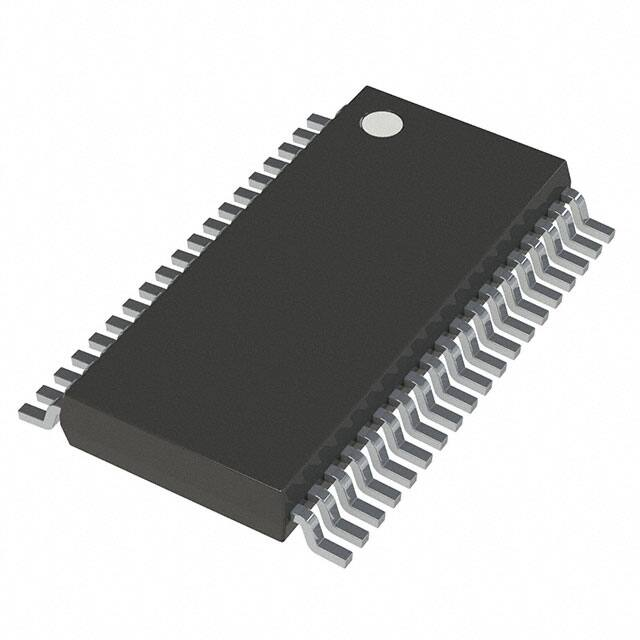
The LTC3376 is available in a compact, 64-ball, 7 mm × 7 mm flip chip ball
grid array (BGA) package. E- and I-grades are specified over an operating
junction temperature range of –40°C to +125°C.
2
RUN1
VINA/B
PGOOD1
BSTA
2
3 V to 20 V
BSTB
IMON1
SWA/B
PGNDA/B
2
0.4 V to 5.5 V
2
FB1+
LTC3376
FB1–
Buck 1 (3 A)
Buck 2 (3 A)
Buck 3 (3 A)
Buck 4 (3 A)
3 V to 20 V
VCC
INTVCC_P
(3 V)
INTVCC
3 V to 5.5 V
(Optional)
EXTVCC
SYNC/MODE
TEMP
CFG[3:0]
RT
GND
Figure 1. LTC3376 simplified block diagram.
Flexibility and Configurability
The inherent flexibility of the LTC3376 allows it to be set up into 15 different
output configurations:
XX
Single inductor, single output 12 A buck where all the power stages are
internally ganged together to produce maximum current output.
XX
Four possible dual-buck combinations with two inductors total with the
total output current summating to 12 A.
XX
Five triple-buck combinations totaling 12 A each with three total inductors.
XX
Five quad-buck configurations of up to 12 A each with four total inductors (see Figure 2).
See Table 1 for a list of the 15 possible output configurations. This flexibility
enables easy adjustment when requirements change in the design process—no need to qualify a new IC when the LTC3376 can remain in place.
Table 1. LTC3376: 15 Examples of 12 A Total Current
Output Configurations
Topology
Output Current Combinations
5 Quad Bucks
3 A, 3 A, 3 A, 3 A,
4.5 A, 3 A, 3 A, 1.5 A,
4.5 A, 4.5 A, 1.5 A, 1.5 A,
6 A, 1.5 A, 3 A, 1.5 A,
7.5 A, 1.5 A, 1.5 A, 1.5 A
5 Triple Bucks
3 A, 4.5 A, 4.5 A,
6 A, 3 A, 3 A,
4.5 A, 6 A, 1.5 A,
7.5 A, 3 A, 1.5 A,
9 A, 1.5 A, 1.5 A
4 Dual Bucks
6 A, 6 A,
7.5 A, 4.5 A,
9 A, 3 A,
10.5 A, 1.5 A
1 Single Buck
12 A
Feature-Rich Systems Demand Flexible and Configurable, 20 V, High Current PMICs
�3 V to 20 V
VCC
VINA
4.7 µF
1 µF
×2
VINB
7.2 V to 20 V
10 µF
×2
BSTA
BSTB
EXTVCC
1.15 MΩ
SWB
FB1+
INTVCC_P
4.7 µF
2.2 µH
SWA
INTVCC
(3 V)
10 µF
5V
3A
22 µF
100 kΩ
LTC3376
FB1–
VINC
RUN1
1 µF
×2
VIND
RUN2
10 µF
×2
4.7 V to 18 V
BSTC
RUN3
BSTD
RUN4
2.2 µH
SWC
1.15 MΩ
SWD
FB2+
PGOOD1
33 µF
PGOOD2
3.3 V, 3 A
Note: 3 A Includes
Input Current of Buck 4.
158 kΩ
FB2–
PGOOD3
PGOOD4
VINE
IMON1
BSTF
IMON3
IMON4
4.99 kΩ
4.99 kΩ
10 µF
×2
3.6 V to 13.6 V
BSTE
IMON2
4.99 kΩ
1 µF
×2
VINF
1.5 µH
SWE
4.99 kΩ
1.05 MΩ
SWF
FB3+
2.5 V
3A
47 µF
200 kΩ
FB3–
TEMP
SYNC/MODE
VING
RT
VINH
402 kΩ
1 µF
×2
10 µF
×2
BSTG
BSTH
680 nH
SWG
Configuration 0000
SWH
CFG0
FB4+
CFG1
CFG2
CFG3
FB4–
GND PGNDA-H
1.8 V
3A
698 kΩ
68 µF
200 kΩ
8
Figure 2. Typical quad-output application circuit.
(a)
(b)
(c)
Figure 3. LTC3376 flip chip package with (a) ball grid array, (b) copper pillars under die, and (c) integrated bypass capacitors.
Excellent Thermal Design and Compact Solution
The LTC3376 enables a compact, thermally efficient solution, in part,
through a unique combination of packaging techniques in its compact,
64-ball, 7 mm × 7 mm flip chip ball grid array package. The internal package construction uses copper pillars in lieu of bond wires. Internal boost
capacitors and an integrated substrate ground plane further improve EMI—
which is less sensitive to PCB layout—simplifying designs and reducing
performance risks (see Figure 3 for details). Furthermore, within the die,
the power devices are arranged to maximize thermal performance—evenly
spreading power dissipation.
Visit analog.com
3
�Figure 4 shows a complete LTC3376 solution in a quad, 4 × 3 A buck (12 A
total output current). Note how compact the total solution size is: the active
area is only ~1.5 cm × 2.9 cm ~ < 4.4 cm2.
The LTC3376 also contains a temperature monitor: die temperature may
be read by sampling the analog TEMP pin voltage. The temperature, T,
indicated by the TEMP pin voltage is given by:
(1)
T = (VTEMP/10 mV) × 1°C
where VTEMP is the voltage on the TEMP pin.
Configurable Buck Regulator Family
Table 2 shows the entire family of configurable quad and octal buck regulators, of which the LTC3376 is the newest member. The LTC3376 has the
highest total output current (up to 12 A) and highest input voltage capability
(up to 20 V).
A product video may be found at analog.com/ltc3376.
Conclusion
Technological advances have driven the increase of feature-rich content
for automotive infotainment, consumer handhelds, industrial equipment,
and medical devices. In many cases, these systems feature input voltages exceeding 5 V and are powered by sophisticated low voltage, high
current digital ICs that have their own set of unique power requirements.
Traditionally, voltage rails and current levels have been supported by a
multitude of discrete power regulator ICs or relatively bulky, overly integrated power management integrated circuits or PMICs. Neither offers
both flexibility and compact size.
Figure 4. LTC3376 demonstration board for a 4 × 3 A buck solution with 5 V, 3.3 V,
2.5 V, and 1.8 V outputs.
Additional System Monitoring, Safety,
and Protection
In addition to its configurability, the LTC3376 includes several safety features
to monitor and protect the systems it powers. Power failure conditions
are reported by each buck’s associated PGOOD pin. Each buck regulator
features a current monitor that produces a current at the IMON pin that is
proportional to the average buck load current.
To prevent thermal damage to the LTC3376 and its surrounding components,
the LTC3376 incorporates an overtemperature function. When the LTC3376
die temperature reaches 165°C (typical), all enabled buck switching regulators are shut down and remain in a shutdown state until the die temperature
falls to 155°C (typical).
Replacing these solutions with a single, quad, or octal multi-output power
IC is a wise choice. The LTC3376 pin-configurable PMIC is an example of
this new generation of multi-output power ICs. It is a 20 V input, digitally
programmable, high efficiency multi-output power supply IC containing four
synchronous buck converters and eight internal power stages (total IOUT up
to 12 A), with low output voltage capability. Since up to 15 different output
current configurations are possible, a system designer can utilize its flexibility and mitigate the impact of inevitable power block system changes and
feature creep. Costly and untimely board or system level requalifications
can be eliminated, reducing product time to market, development costs as
well as upgrade time and costs.
Table 2. ADI’s Power by Linear Family of Configurable Quad and Octal Buck Regulators
ADI/LTC
Parameters
ADI/LTC
Linear
Linear
Linear
Linear
LTC3376
LTC3374A
LTC3374
LTC3375
LTC3371
LTC3370
Quad buck
Octal buck
Octal buck
Octal buck
Quad buck
Quad buck
4
8
8
8 + ext HV
controller
4
4
Total Output Current
8 × 1.5 A = 12 A
8×1A=8A
8×1A=8A
8×1A=8A
Up to 8 A
Up to 8 A
Output Voltage
VOUT: 0.4 V to 0.83
× VIN
VOUT: 0.8 V to VIN
VOUT: 0.8 V to VIN
VOUT: 0.425 V to VIN
VOUT: 0.8 V to VIN
VOUT: 0.8 V to VIN
Configurations
15
15
15
15
8
8
Parallelable Buck Switchers
(Single Inductor)
Yes, up to 4
Yes, up to 4
Yes, up to 4
Yes, up to 4
Yes, up to 4
Yes, up to 4
Input Voltage
3 V to 20 V
2.25 V to 5.5 V
2.25 V to 5.5 V
2.25 V to 5.5 V
2.25 V to 5.5 V
dc-to-dc converters
2.7 V to 5.5 V Vcc
2.25 V to 5.5 V
dc-to-dc converters
2.7 V to 5.5 V Vcc
Operating Quiescent Current
28 µA (1 channel)
63 µA (1 channel)
63 µA (1 channel)
68 µA (1 channel)
68 µA (1 channel)
63 µA (1 channel)
Frequency/Sync
1 MHz to 3 MHz
1 MHz to 3 MHz
1 MHz to 3 MHz
1 MHz to 3 MHz
1 MHz to 3 MHz
1 MHz to 3 MHz
Simple
Simple
Simple
I2C
Simple
Simple
7 × 7 FC,
64-ball BGA
5 × 7, 38-lead QFN,
38-lead TSSOP-E
5 × 7, 38-lead QFN,
38-lead TSSOP-E
7 × 7,
48-lead QFN
5 × 7, 38-lead QFN,
38-lead TSSOP-E
5 × 5, 32-lead QFN
Topology
Number of Channels
I2C/Simple Interface
Package (mm)
4
Feature-Rich Systems Demand Flexible and Configurable, 20 V, High Current PMICs
�About the Author
Steve Knoth is a senior product marketing manager in Analog Devices’
Power Group. He is responsible for all power management integrated circuit (PMIC) products, low dropout (LDO) regulators, battery
chargers, charge pumps, charge pump-based LED drivers, supercapacitor chargers, low voltage monolithic switching regulators, and
ideal diode devices. Prior to joining Analog Devices in 2004, Steve
held various marketing and product engineering positions since
1990 at Micro Power Systems and Micrel Semiconductor. He earned
his bachelor’s degree in electrical engineering in 1988 and a master’s degree in physics in 1995, both from San Jose State University.
Steve also received an M.B.A. in technology management from the
University of Phoenix in 2000. In addition to enjoying time with his
kids, Steve is an avid music lover and can be found tinkering with
pinball and arcade games or muscle cars, and buying, selling, and
collecting vintage toys, movie, sports, and automotive memorabilia.
He can be reached at steve.knoth@analog.com.
Online Support
Community
Engage with the
Analog Devices technology experts in our online support
community. Ask your tough design questions, browse FAQs,
or join a conversation.
Visit ez.analog.com
©2019 Analog Devices, Inc. All rights reserved.
Trademarks and registered trademarks are
the property of their respective owners.
For regional headquarters, sales, and distributors or
to contact customer service and technical support,
visit analog.com/contact.
TA21693-10/19
Ask our ADI technology experts tough questions, browse
FAQs, or join a conversation at the EngineerZone Online
Support Community. Visit ez.analog.com.
VISIT ANALOG.COM
�