LTC3427
500mA, 1.25MHz
Synchronous Step-Up
DC/DC Converter in
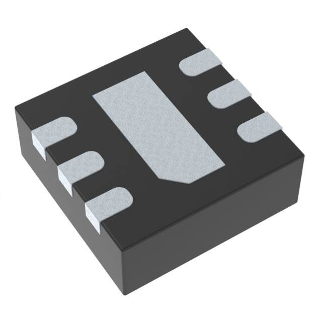
2mm × 2mm DFN Package
U
FEATURES
DESCRIPTIO
■
The LTC®3427 is the industry’s first high efficiency, fixed
frequency, step-up DC/DC converter with true output
disconnect in a 6-lead 2mm × 2mm DFN package. Requiring minimal external components, the LTC3427 operates
from an input voltage as low as 1.8V. The LTC3427
contains an internal 0.525Ω N-channel MOSFET switch
and a 0.575Ω P-channel MOSFET synchronous rectifier,
which enables it to supply 200mA at 3.3V from a 2-cell
alkaline battery input.
■
■
■
■
■
■
■
■
■
■
■
■
■
High Efficiency: Up to 94%
3.3V at 200mA from Two Alkaline Cells
5V at 200mA from a Single Li-Ion Cell
Inrush Current Limiting and Soft-Start
Output Disconnect in Shutdown
1.8V to 5V VIN Range
1.8V to 5.25V VOUT Range
1.25MHz Fixed Frequency, Low Noise PWM
Internal Synchronous Rectifier
Logic Controlled Shutdown ( VOUT
PMOS LDO MODE
50
0.50
–45 –30 –15
0 15 30 45 60
TEMPERATURE (°C)
75
1.23
–45 –30 –15
90
0 15 30 45 60
TEMPERATURE (°C)
75
40
90
1.5
3.5
VIN (V)
2.5
3427 G07
3427 G06
Frequency Accuracy
vs Temperature
4.5
3427 G08
SW Pin Anti-Ringing Operation
1.35
FREQUENCY (MHz)
VIN = 2.4V
VOUT = 3.3V
1.30
INDUCTOR
CURRENT
50mA/DIV
1.25
SW
2V/DIV
VIN = 1.8V
VOUT = 3.3V
COUT = 4.7µF
L = 4.7µH
1.20
1.15
–45 –30 –15
0 15 30 45 60
TEMPERATURE (°C)
75
3427 G10
200ns/DIV
90
3427 G09
RDS(ON) vs Temperature
VIN Supply Current (No Load)
0.45
0.70
VIN = 2.4V
VOUT = 3.3V
TA = 25°C
VIN = VOUT = VFB
VIN SUPPLY CURRENT (mA)
0.65
RDS(ON) (Ω)
0.60
0.40
PMOS
0.55
NMOS
0.50
0.35
0.45
0.40
0.35
–45 –30 –15
0 15 30 45 60
TEMPERATURE (°C)
75
90
3427 G11
0.30
1.5
2.5
3.5
VIN (V)
4.5
5.5
3427 G12
3427fa
4
�LTC3427
U
U
U
PI FU CTIO S
SW (Pin 1): Switch Pin for the Inductor Connection.
Minimize trace length between SW and the inductor. For
discontinuous inductor current, an internal 200Ω impedance is connected from SW to VIN to eliminate high
frequency ringing, reducing EMI radiation.
GND (Pin 2): Signal and Power Ground. Provide a short,
direct PCB path between GND and the (–) side of the input
and output capacitor(s).
FB (Pin 5): Feedback Input to the Error Amplifier. Connect
resistor divider tap to this pin. Referring to the Block
Diagram, VOUT can be adjusted from 1.8V to 5.25V by:
⎛ R1⎞
VOUT = 1.24V • ⎜ 1+ ⎟
⎝ R2 ⎠
VIN (Pin 3): Input Supply Voltage. Connect VIN to the input
supply and decouple with a 2.2µF or larger ceramic
capacitor as close to VIN as possible.
VOUT (Pin 6): Output Voltage Sense Input and Drain of the
Internal Synchronous Rectifier MOSFET. Driver bias is
derived from VOUT. PCB trace length from VOUT to the
output filter capacitor(s) should be as short and wide as
possible.
SHDN (Pin 4): Shutdown Input. Less than 350mV on
SHDN shuts down the LTC3427. Placing 1V or more on
SHDN enables the LTC3427.
Exposed Pad (Pin 7): Ground for the LTC3427. This pin
must be soldered to the PCB ground plane for electrical
connection and rated thermal performance.
W
BLOCK DIAGRA
L1
4.7µH
+
CIN
2.2µF
4
3
1
VIN
SHDN
SW
VIN
SHUTDOWN
AND
VBIAS
OPTIONAL
BULK CONTROL
SIGNALS
ANTIRING
VOUT
VOUT
1.8V TO 5.25V
6
SHDN
PWM
LOGIC
AND
DRIVERS
+
–
IZERO
COMP
CURRENT
SENSE
1.24V
REFERENCE
PWM
COMP
– + –
VIN
1.8V TO 5V
THERMAL
SHUTDOWN
ILIM
REF
Σ
1V
GAIN ERROR
AMPLIFIER
R1
+
FB
–
1.24V
COUT
4.7µF
5
R2
+
+
SLOPE COMPENSATION
START-UP
SOFT-START
OSCILLATOR
7
EXPOSED PAD
GND
2
3427 BD
3427fa
5
�LTC3427
U
OPERATIO
(Refer to Block Diagram)
LOW NOISE FIXED FREQUENCY OPERATION
of input or output voltage. The current signal is blanked for
approximately 25ns to enhance noise rejection.
Shutdown
The LTC3427 is shut down by pulling the SHDN pin below
0.35V, and activated by pulling the SHDN pin above 1V.
Note that SHDN can be driven above VIN or VOUT as long
as it is limited to less than the absolute maximum rating.
Current Limit
The current limit circuitry shuts off the internal N-channel
MOSFET switch when the current limit threshold is reached.
The current limit comparator delay to output is typically
40ns.
Soft-Start
The LTC3427 provides soft-start by ramping the peak
inductor current from zero to its peak value of 500mA. The
soft-start time is typically 2ms. A soft-start cycle is reinitiated in the event of a commanded shutdown or a
thermal shutdown.
Zero Current Comparator
The zero current comparator monitors the inductor current to the output and shuts off the synchronous rectifier
once this current reduces to approximately 20mA.
Anti-Ringing Control
Oscillator
The frequency of operation is set by an internal oscillator
to 1.25MHz for the LTC3427.
Error Amplifier
The error amplifier is a transconductance type with its
positive input internally connected to the 1.24V reference
and the negative input connected to FB. Internal clamps
limit the minimum and maximum error amplifier output
voltage for improved large-signal transient response.
Power converter control loop compensation is provided
internally by the error amplifier. A voltage divider from
VOUT to ground programs the output voltage via FB from
1.8V to 5.25V.
⎛ R1⎞
VOUT = 1.24V • ⎜ 1+ ⎟
⎝ R2 ⎠
The anti-ringing control connects a resistor across the
inductor to damp the ringing on the SW pin in discontinuous conduction mode. The LCSW ringing (L = Inductor,
CSW = capacitance on the SW pin) is low energy, but can
cause EMI radiation.
Output Disconnect and Inrush Limiting
The LTC3427 provides true output disconnect by eliminating body diode conduction of the internal P-channel
MOSFET rectifier. This allows VOUT to go to zero volts
during shutdown without drawing any current from the
input source. It also provides inrush current limiting at
turn-on, minimizing surge currents seen by the input
supply. Note that to obtain the advantages of output
disconnect, there must not be any external Schottky diode
connected between SW and VOUT.
Thermal Shutdown
The error amplifier also provides a soft-start feature
internal to the device.
Current Sensing
Lossless current sensing converts the peak current signal
of the N-channel MOSFET switch into a voltage that is
summed with the internal slope compensation. The
summed signal is compared to the error amplifier output to
provide a peak current control command for the PWM. Peak
switch current is limited to 500mA minimum, independent
If the die temperature reaches approximately 145°C, the
part will go into thermal shutdown. All switches will be
turned off. The device will be enabled and initiate a softstart sequence when the die temperature drops by
approximately 10°C.
Note: Due to the high frequency operation of the LTC3427,
board layout is extremely critical to minimize transients
due to stray inductance. Keep the output filter capacitor as
close as possible to the VOUT pin and use very low ESR/
ESL ceramic capacitors tied to a good ground plane.
3427fa
6
�LTC3427
U
W
U U
APPLICATIO S I FOR ATIO
LTC3427
SW 1
6 VOUT
GND 2
+
5 FB
VIN 3
MINIMIZE
TRACE ON FB
4 SHDN
VIN
MULTIPLE VIAS
TO GROUND PLANE
3427 F01
Figure 1. Recommended Component Placement for a Single Layer Board. Traces Carrying High Current are Direct (GND, SW, VIN,
VOUT). Trace Area at FB is Kept Low. Lead Length to Battery Should be Kept Short. VIN and VOUT Ceramic Capacitors Should be as
Close to the LTC3427 as Possible. A Multilayer Board with a Separate Ground Plane is Ideal, but not Absolutely Necessary
COMPONENT SELECTION
Inductor Selection
The LTC3427 can utilize small surface mount and chip
inductors due to its fast 1.25MHz switching frequency. A
minimum inductance value of 3.3µH is necessary for 3.6V
and lower voltage applications and a 4.7µH for output
voltages greater than 3.6V. Larger values of inductance
will allow greater output current capability by reducing the
inductor ripple current. Increasing the inductance above
10µH will increase size while providing little improvement
in output current capability.
The approximate output current capability of the LTC3427
vs Inductance value is given below in Equation 1 and
illustrated graphically in Figure 2.
V •D ⎞
⎛
IOUT(MAX ) = n • ⎜ IP – IN ⎟ • (1 – D)
⎝
f • L • 2⎠
where:
n = estimated efficiency
IP = peak current limit value (0.5A min)
VIN = input (battery) voltage
D = steady-state duty ratio = (VOUT – VIN)/VOUT
f = switching frequency (1.25MHz typical)
L = inductance value
(1)
The inductor current ripple is typically set for 20% to 40%
of the maximum inductor current (IP). High frequency
ferrite core inductor materials reduce frequency dependent power losses compared to cheaper powdered iron
types, improving efficiency. The inductor should have low
ESR (series resistance of the windings) to reduce the I2R
power losses, and must be able to handle the peak
inductor current without saturating. Molded chokes and
some chip inductors usually do not have enough core to
support the peak inductor currents of greater than 500mA
seen on the LTC3427. To minimize radiated noise, use a
toroid, pot core or shielded bobbin inductor. See Table 1
for suggested suppliers.
Output and Input Capacitor Selection
Low ESR (equivalent series resistance) capacitors should
be used to minimize the output voltage ripple. Multilayer
ceramic capacitors are an excellent choice as they have
extremely low ESR and are available in small footprints. A
2.2µF to 10µF output capacitor is sufficient for most
applications. Larger values up to 22µF may be used to
obtain extremely low output voltage ripple and improve
transient response. An additional phase lead capacitor
may be required with output capacitors larger than 10µF to
maintain acceptable phase margin. X5R and X7R dielectric materials are preferred for their ability to maintain
capacitance over wide voltage and temperature ranges.
3427fa
7
�LTC3427
U
W
U U
APPLICATIO S I FOR ATIO
Table 1. Inductor Vendor Information
SUPPLIER
PHONE
FAX
WEBSITE
Murata
USA: (814) 237-1431
(800) 831-9172
USA: (814) 238-0490
www.murata.com
Sumida
USA: (847) 956-0666
Japan: 81-3-3607-5111
USA: (847) 956-0702
Japan: 81-3-3607-5144
www.sumida.com
Coilcraft
(847) 639-6400
(847) 639-1469
www.coilcraft.com
CoEv Magnetics
(800) 227-7040
(650) 361-2508
www.circuitprotection.com/magnetics.asp
TDK
(847) 803-6100
(847) 803-6296
www.component.tdk.com
TOKO
(847) 297-0070
(847) 669-7864
www.toko.com
Wurth
(201) 785-8800
(201) 785-8810
www.we-online.com
0.280
Table 2. Capacitor Vendor Information
1.8V TO 3V
0.260
3.1V TO 5V
OUTPUT CURRENT (A)
0.240
1.8V TO 3.3V
0.220
SUPPLIER PHONE
FAX
WEBSITE
AVX
(803) 448-9411
(803) 448-1943
www.avxcorp.com
Sanyo
(619) 661-6322
(619) 661-1055
www.sanyovideo.com
TDK
(847) 803-6100
(847) 803-629
www.component.
tdk.com
Murata
USA:
(814) 237-1431
(800) 831-9172
USA:
(814) 238-0490
www.murata.com
Taiyo
Yuden
(408) 573-4150
(408) 573-4159
www.t-yuden.com
1.8V TO 3.6V
0.200
0.180
0.160
1.8V TO 5V
0.140
0.120
0.100
3
5
7
9 11 13 15 17 19 21 23
INDUCTANCE (µH)
3427 F02
Figure 2. Maximum Output Current vs
Inductance Based on 90% Efficiency
Low ESR input capacitors reduce input switching noise
and reduce the peak current drawn from the battery. It
follows that ceramic capacitors are also a good choice for
input decoupling and should be located as close as possible to the device. A 2.2µF input capacitor is sufficient for
virtually any application. Larger values may be used without limitations. Table 2 shows a list of several ceramic
capacitor manufacturers. Consult the manufacturers directly for detailed information on their entire selection of
ceramic capacitors.
Thermal Considerations
To deliver the power that the LTC3427 is capable of, it is
imperative that a good thermal path be provided to dissipate the heat generated within the package. This can be
accomplished by taking advantage of the large thermal
pad on the underside of the LTC3427. It is recommended
that multiple vias in the printed circuit board be used to
conduct heat away from the LTC3427 and into the copper
plane with as much area as possible. In the event that the
junction temperature gets too high, the LTC3427 will go
into thermal shutdown and all switching will stop until the
internal temperature drops at which point a soft-start cycle
will be initiated.
3427fa
8
�LTC3427
U
W
U U
APPLICATIO S I FOR ATIO
VIN > VOUT Operation
Short-Circuit Protection
The LTC3427 will maintain voltage regulation when the
input voltage is above the output voltage. This is achieved
by terminating the switching of the synchronous P-channel MOSFET and applying VIN statically on its gate. This
will ensure the volt • seconds across the inductor reverse
during the time current is flowing to the output. Since this
mode will dissipate more power in the LTC3427, the
maximum output current is limited in order to maintain an
acceptable junction temperature and is given by:
The LTC3427 output disconnect feature allows output
short circuit while maintaining a maximum internally set
current limit. However, the LTC3427 also incorporates
internal features such as current limit foldback and thermal shutdown for protection from an excessive overload
or short circuit. During a prolonged short circuit the
current limit folds back to a typical value of approximately
400mA should VOUT drop below 950mV. This 400mA
current limit remains in effect until VOUT exceeds approximately 1V, at which time the nominally internally set
current limit is restored.
IOUT(MAX ) =
125 – TA
85 • ⎡⎣( VIN + 1.5) – VOUT ⎤⎦
where TA = ambient temperature.
For example at VIN = 4.5V, VOUT = 3.3V, and TA = 85°C, the
maximum output current is 145mA.
3427fa
9
�LTC3427
U
TYPICAL APPLICATIO S
L1
4.7µH
2-CELL
ALKALINE
+
2-Cell to 3.3V Efficiency
100
CIN
2.2µF
95
VIN
LTC3427
OFF ON
SHDN
VOUT
1000k
VOUT
3.3V
200mA
COUT
4.7µF
FB
GND
VIN = 3.1V
90
SW
EFFICIENCY (%)
VIN
1.8V TO 3.2V
604k
VIN = 2.4V
85
80
VIN = 1.8V
75
70
65
60
CIN: TAIYO YUDEN X5R JMK212BJ225MD
COUT: TAIYO YUDEN X5R JMK212BJ475MD
L1: TDK RLF7030T-4R7M3R4
3427 F03a
55
50
10
100
LOAD CURRENT (mA)
1
Figure 3. 2-Cell Alkaline to 3.3V Synchronous Boost Converter
1000
3427 G01
2-Cell to 5V Efficiency
L1
4.7µH
2-CELL
ALKALINE
+
100
95
CIN
2.2µF
VIN
90
SW
LTC3427
OFF ON
SHDN
VOUT
5V
150mA
VOUT
1000k
GND
COUT
4.7µF
FB
EFFICIENCY (%)
VIN
1.8V TO 3.2V
VIN = 3.2V
85
VIN = 2.4V
80
75
VIN = 1.8V
70
65
332k
60
CIN: TAIYO YUDEN X5R JMK212BJ225MD
COUT: TAIYO YUDEN X5R JMK212BJ475MD
L1: TDK RLF7030T-4R7M3R4
55
3427 F04a
50
10
100
LOAD CURRENT (mA)
1
Figure 4. 2-Cell Alkaline to 5V Synchronous
Boost Converter with Output Disconnect
3427 G03
Li-Ion to 5V Synchronous Boost Converter
Li-Ion to 5V Efficiency
100
L1
4.7µH
Li-Ion
+
95
VIN
SW
LTC3427
OFF ON
SHDN
VOUT
5V
250mA
VOUT
1000k
CIN: TAIYO YUDEN X5R JMK212BJ225MD
COUT: TAIYO YUDEN X5R JMK212BJ475MD
L1: TDK RLF7030T-4R7M3R4
VIN = 4.2V
90
CIN
2.2µF
GND
COUT
4.7µF
FB
332k
EFFICIENCY (%)
VIN
3.1V TO 4.2V
1000
VIN = 3.6V
85
80
VIN = 3.1V
75
70
65
60
55
3427 TA02a
50
1
10
100
LOAD CURRENT (mA)
1000
3427 G02
3427fa
10
�LTC3427
U
PACKAGE DESCRIPTIO
DC Package
6-Lead Plastic DFN (2mm × 2mm)
(Reference LTC DWG # 05-08-1703)
0.675 ±0.05
2.50 ±0.05
1.15 ±0.05 0.61 ±0.05
(2 SIDES)
PACKAGE
OUTLINE
0.25 ± 0.05
0.50 BSC
1.42 ±0.05
(2 SIDES)
RECOMMENDED SOLDER PAD PITCH AND DIMENSIONS
R = 0.115
TYP
0.56 ± 0.05
(2 SIDES)
0.38 ± 0.05
4
6
2.00 ±0.10
(4 SIDES)
PIN 1 BAR
TOP MARK
(SEE NOTE 6)
PIN 1
CHAMFER OF
EXPOSED PAD
3
0.200 REF
0.75 ±0.05
1
(DC6) DFN 1103
0.25 ± 0.05
0.50 BSC
1.37 ±0.05
(2 SIDES)
0.00 – 0.05
BOTTOM VIEW—EXPOSED PAD
NOTE:
1. DRAWING TO BE MADE A JEDEC PACKAGE OUTLINE M0-229 VARIATION OF (WCCD-2)
2. DRAWING NOT TO SCALE
3. ALL DIMENSIONS ARE IN MILLIMETERS
4. DIMENSIONS OF EXPOSED PAD ON BOTTOM OF PACKAGE DO NOT INCLUDE
MOLD FLASH. MOLD FLASH, IF PRESENT, SHALL NOT EXCEED 0.15mm ON ANY SIDE
5. EXPOSED PAD SHALL BE SOLDER PLATED
6. SHADED AREA IS ONLY A REFERENCE FOR PIN 1 LOCATION ON THE
TOP AND BOTTOM OF PACKAGE
3427fa
Information furnished by Linear Technology Corporation is believed to be accurate and reliable.
However, no responsibility is assumed for its use. Linear Technology Corporation makes no representation that the interconnection of its circuits as described herein will not infringe on existing patent rights.
11
�LTC3427
RELATED PARTS
PART NUMBER
DESCRIPTION
COMMENTS
LT®1613
800mA ISW, 1.4MHz, Step-Up DC/DC Converter
VIN: 1.1V to 10V, VOUT(MAX) = 34V, IQ = 3mA, ISD < 1µA,
5-Lead SOT-23 Package
LT1615
350mA ISW, Micropower, Step-Up DC/DC Converter
VIN: 1.2V to 15V, VOUT(MAX) = 34V, IQ = 20µA, ISD < 1µA,
ThinSOTTM Package
LT1618
1.5A ISW, 1.4MHz, Constant Current/Constant Voltage
Step-Up DC/DC Converter
VIN: 1.6V to 18V, VOUT(MAX) = 35V, IQ = 1.8mA, ISD < 1µA,
DFN, MSOP Packages
LT1930/LT1930A
1A ISW, 1.2MHz/2.2MHZ, Step-Up DC/DC Converters
VIN: 2.6V to 16V, VOUT(MAX) = 34V, IQ = 4.2mA/5.5mA, ISD < 1µA,
ThinSOT Package
LTC3400/LTC3400B
600mA ISW, 1.2MHz, Synchronous Step-Up
DC/DC Converters
92% Efficiency VIN: 0.85V to 5V, VOUT(MAX) = 5V, IQ = 19µA/300µA,
ISD < 1µA, ThinSOT Package
LTC3401
1A ISW, 3MHz, Synchronous Step-Up DC/DC Converter
97% Efficiency VIN: 0.5V to 5V, VOUT(MAX) = 6V, IQ = 38µA, ISD < 1µA,
10-Lead MS Package
LTC3402
2A ISW, 3MHz, Synchronous Step-Up DC/DC Converter
97% Efficiency VIN: 0.5V to 5V, VOUT(MAX) = 6V, IQ = 38µA, ISD < 1µA,
10-Lead MS Package
LTC3421
3A ISW, 3MHz, Synchronous Step-Up
DC/DC Converter with Output Disconnect
95% Efficiency VIN: 0.5V to 4.5V, VOUT(MAX) = 5.25V, IQ = 12µA,
ISD < 1µA, QFN24 Package
LTC3422
1.5A ISW, 3MHz Synchronous Step-Up
DC/DC Converter with Output Disconnect
95% Efficiency VIN: 0.5V to 4.5V, VOUT(MAX) = 5.25V, IQ = 25µA,
ISD < 1µA, 3mm × 3mm DFN Package
LTC3423/LTC3424
1A/2A ISW, 3MHz, Synchronous Step-Up DC/DC Converter
95% Efficiency VIN: 0.5V to 5.5V, VOUT(MAX) = 5.5V, IQ = 38µA,
ISD < 1µA, 10-Lead MS Package
LTC3426
2A ISW, 1.2MHz, Step-Up DC/DC Converter
92% Efficiency VIN: 1.6V to 4.3V, VOUT(MAX) = 5V, ISD < 1µA,
SOT-23 Package
LTC3428
500mA ISW, 1.25MHz/2.5MHz, Synchronous Step-Up
DC/DC Converters with Output Disconnect
92% Efficiency VIN: 1.8V to 5V, VOUT(MAX) = 5.25V, ISD < 1µA,
2mm × 2mm DFN Package
LTC3429
600mA ISW, 500kHz, Synchronous Step-Up DC/DC
Converter with Output Disconnect and Soft-Start
96% Efficiency VIN: 0.5V to 4.4V, VOUT(MAX) = 5V, IQ = 20µA/300µA,
ISD < 1µA, ThinSOT Package
LTC3458
1.4A ISW, 1.5MHz, Synchronous Step-Up DC/DC
Converter/Output Disconnect/Burst Mode Operation
93% Efficiency VIN: 1.5V to 6V, VOUT(MAX) = 7.5V, IQ = 15µA,
ISD < 1µA, DFN12 Package
LTC3458L
1.7A ISW, 1.5MHz, Synchronous Step-Up DC/DC Converter
with Output Disconnect, Automatic Burst Mode® Operation
94% Efficiency VOUT(MAX) = 6V, IQ = 12µA, DFN12 Package
LTC3459
70mA ISW, 10V Micropower Synchronous Boost
Converter/Output Disconnect/Burst Mode Operation
VIN: 1.5V to 5.5V, VOUT(MAX) = 10V, IQ = 10µA, ISD < 1µA,
ThinSOT Package
LTC3525-3.3
LTC3525-5
400mA Micropower Synchronous Step-Up
DC/DC Converter with Output Disconnect
95% Efficiency VIN: 1V to 4.5V, VOUT(MAX) = 3.3V or 5V, IQ = 7µA,
ISD < 1µA, SC-70 Package
ThinSOT is a trademark of Linear Technology Corporation. Burst Mode is a registered trademark of Linear Technology Corporation.
3427fa
12
Linear Technology Corporation
LT 0406 REV A • PRINTED IN THE USA
1630 McCarthy Blvd., Milpitas, CA 95035-7417
(408) 432-1900 ● FAX: (408) 434-0507
●
www.linear.com
© LINEAR TECHNOLOGY CORPORATION 2005
�


 工商网监
湘ICP备2023018690号
工商网监
湘ICP备2023018690号

