LTC3452
Synchronous Buck-Boost
MAIN/CAMERA White LED Driver
U
FEATURES
■
■
■
■
■
■
■
■
■
■
■
■
DESCRIPTIO
High Efficiency: ≥85% Over Entire Li-Ion Battery
Range
Wide VIN Range: 2.7V to 5.5V
Independent MAIN/CAMERA Current Control
Up to 425mA Continuous Output Current
Internal Soft-Start
Open/Shorted LED Protection
PWM Brightness Control
LED Current Matching Typically 1.2V). For ENL voltage
VIN(MIN)2 •
( VOUT – VIN(MIN) ) • 100%
f • IOUT(MAX ) • %Ripple • VOUT 2
Table 3. Capacitor Vendor Information
SUPPLIER
WEB SITE
AVX
www.avxcorp.com
Sanyo
www.sanyovideo.com
Taiyo Yuden
www.t-yuden.com
TDK
www.component.tdk.com
and in buck mode is:
L>
(
)
VOUT • VIN(MAX ) – VOUT • 100%
f • IOUT(MAX ) • %Ripple • VIN(MAX )
where:
f = operating frequency, Hz
%Ripple = allowable inductor current ripple, %
VIN(MIN) = minimum input voltage, V
VIN(MAX) = maximum input voltage, V
VOUT = output voltage, V
IOUT(MAX) = maximum output load current
For high efficiency, choose an inductor with a high frequency core material, such as ferrite, to reduce core loses.
The inductor should have low ESR (equivalent series
resistance) to reduce the I2R losses, and must be able to
handle the peak inductor current without saturating. Molded
chokes or chip inductors usually do not have enough core
to support peak inductor currents >1A. To minimize radiated noise, use a toroid, pot core or shielded bobbin
inductor. For the white LED application, a 4.7µH inductor
value is recommended. See Table 2 for a list of component
suppliers.
Table 2. Inductor Vendor Information
SUPPLIER
WEB SITE
Coilcraft
www.coilcraft.com
Cooper/Coiltronics
www.cooperet.com
Murata
www.murata.com
Sumida
www.japanlink.com/sumida
Vishay-Dale
www.vishay.com
Output Capacitor Selection
The bulk value of the capacitor is set to reduce the ripple
due to charge into the capacitor each cycle. The steady
state ripple due to charge is given by:
%Ripple _ Boost =
%Ripple _ Buck =
(
)
IOUT(MAX ) • VOUT – VIN(MIN) • 100
COUT • VOUT 2 • f
%
( VIN(MAX) – VOUT ) • 100 %
8 • VIN(MAX ) • f 2 • L • COUT
where COUT = output filter capacitor, F
The output capacitance is usually many times larger in
order to handle the transient response of the converter.
For a rule of thumb, the ratio of the operating frequency to
the unity-gain bandwidth of the converter is the amount
the output capacitance will have to increase from the
above calculations in order to maintain the desired transient response.
The other component of ripple is due to the ESR (equivalent series resistance) of the output capacitor. Low ESR
capacitors should be used to minimize output voltage
ripple. For surface mount applications, Taiyo Yuden, TDK,
AVX ceramic capacitors, AVX TPS series tantalum capacitors or Sanyo POSCAP are recommended. For the white
LED application, a 4.7µF capacitor value is recommended.
See Table 3 for a list of component suppliers.
3452f
11
�LTC3452
U
W
U U
APPLICATIO S I FOR ATIO
Optional Schottky Diodes
Schottky diodes across the synchronous switches B and
D are not required, but provide a lower drop during the
break-before-make time (typically 20ns) of the NMOS to
PMOS transition, improving efficiency. Use a Schottky
diode such as an MBRM120T3 or equivalent. Do not use
ordinary rectifier diodes, since the slow recovery times
will compromise efficiency.
The unity-gain frequency of the error amplifier with the
Type I compensation is given by:
fUG =
gm
2 • π • CVC
where gm is the error amp transconductance (typically
1/5.2k) and CVC is the external capacitor to GND at the
VC pin. For the white LED application, a 0.1µF or greater
capacitor value is recommended.
Closing the Feedback Loop
The LTC3452 incorporates voltage mode PWM control.
The control to output gain varies with operation region
(Buck, Boost, Buck/Boost), but is usually no greater than
15. The output filter exhibits a double pole response
given by:
fFILTER _ POLE =
1
Hz
2 • π • L • COUT
where COUT is the output filter capacitor.
The output filter zero is given by:
fFILTER _ ZERO =
1
2 • π • RESR • COUT
Hz
where RESR is the capacitor equivalent series resistance.
A troublesome feature in Boost mode is the right-half
plane zero (RHP), and is given by:
2
fRHPZ
VIN
=
Hz
2 • π • IOUT • L • VOUT
The loop gain is typically rolled off before the RHP zero
frequency.
A simple Type I compensation network can be incorporated to stabilize the loop but at a cost of reduced bandwidth and slower transient response. To ensure proper
phase margin, the loop is required to be crossed over a
decade before the LC double pole.
Paralleling LED Outputs for Higher Current
Two or more LED output pins can be connected together
in parallel to achieve higher output current in fewer than 7
LEDs. For a very high power LED such as a LumiLED, all
7 outputs can be connected in parallel for maximum total
output current, as shown in the back page application of
this data sheet.
Maximum LED Current
As described in the Operation section, the maximum
output LED currents are equal to:
⎛ 0.8 V ⎞
IMAXL = 256⎜
⎟
⎝ RISETL ⎠
and
⎛ 0.8 V ⎞
IMAXH = 768⎜
⎟
⎝ RISETH ⎠
Since the maximum LED current for the low power bank is
25mA, this sets a minimum limit on RISETL of:
⎛ 0.8 V ⎞
RMINL = 256 ⎜
= 8192Ω
⎝ 25mA ⎟⎠
Similarly, for the high power bank:
⎛ 0.8 V ⎞
= 4096Ω
RMINH = 768 ⎜
⎝ 150mA ⎟⎠
In addition, since the maximum continuous output current
for the buck-boost is limited to 425mA, this may impose
higher resistor value minimums if all outputs are used.
3452f
12
�LTC3452
U
W
U U
APPLICATIO S I FOR ATIO
Although the LTC3452 can safely provide this current
continuously, the external LED(s) may not be rated for this
high a level of continuous current. Higher current levels in
a single LED are generally reserved for pulsed applications, such as LED camera flash. This is accomplished by
programming a high current with one or both of the RISET
resistors and pulsing the appropriate enable pin or pins as
shown in the back page application.
VIN
Varying LED Brightness Linearly
Continuously variable LED brightness control can be
achieved by interfacing directly to one or both of the ISET
pins. Figure 3 shows four such methods employing a
voltage DAC, a current DAC, a simple potentiometer or a
PWM input applied to the ISETL pin for controlling the low
power bank LED currents. These four techniques can be
similarly applied to the ISETH pin for controlling the high
power bank LED currents.
VOUT
ENL
VIN
VOUT
ENL
LEDL1
LTC3452
ISETL
VOLTAGE
DAC
ISETL
LEDL5
0.8V – VDAC
ILED = 256
RSET
RSET ≥ RMINL
LEDL1
LTC3452
ILED = 256 • IDAC
0.8V
RMINL
IDAC ≤
CURRENT
DAC
VDAC
LEDL5
(3a)
VIN
(3b)
VOUT
ENL
VIN
VOUT
ENL
LEDL1
LTC3452
ISETL
ISETL
LEDL5
0.8V
ILED = 256
RMINL + RPOT
RMINL
LEDL1
LTC3452
RSET
100
RSET ≥ RMINL
LEDL5
ILED = 256
VPWM
RPOT
= 256
1µF
0.8V – VPWM
RSET
0.8V – (DC% • VDVCC)
RSET
DVCC
fPWM ≥ 10kHz
(3c)
(3d)
3452 F03
Figure 3. Additional Brightness Control Methods: (3a) Using Voltage DAC,
(3b) Using Current DAC, (3c) Using Potentiometer, (3d) Using PWM Input
3452f
13
�LTC3452
U
W
U U
APPLICATIO S I FOR ATIO
Unused Outputs
If fewer than 7 LED pins are to be used, unused LEDx pins
should be connected to VOUT. The LTC3452 senses which
current source outputs are not being used and shuts off
the corresponding output currents to save power. A small
trickle current (10µA: low power bank, 30µA: high power
bank) is still applied to unused outputs to detect if a white
LED is later switched in and also to distinguish unused
outputs from used outputs during start-up.
LED Failure Modes
If an individual LED fails as a short circuit, the current
source biasing it is shut off to save power. This is the same
operation as described previously (if the output were
initially designated unused at power-up by connecting its
LEDx pin to VOUT). Efficiency is not materially affected.
If an individual LED fails as an open circuit, the control loop
will initially attempt to regulate off of its current source
feedback signal, since it will appear to be the one requiring
the largest forward voltage drop to run at its programmed
current. This will drive VOUT higher. As the open circuited
LED will never accept its programmed current, VOUT must
be voltage-limited by means of a secondary control loop.
The LTC3452 limits VOUT to 4.5V in this failure mode. The
other LEDs will still remain biased at the correct programmed current but the overall circuit efficiency will
decrease.
3452f
14
�LTC3452
U
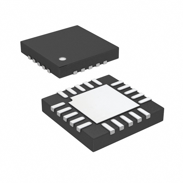
PACKAGE DESCRIPTIO
UF Package
20-Lead Plastic QFN (4mm × 4mm)
(Reference LTC DWG # 05-08-1710)
0.70 ±0.05
4.50 ± 0.05
3.10 ± 0.05
2.45 ± 0.05
(4 SIDES)
PACKAGE OUTLINE
0.25 ±0.05
0.50 BSC
RECOMMENDED SOLDER PAD PITCH AND DIMENSIONS
BOTTOM VIEW—EXPOSED PAD
4.00 ± 0.10
(4 SIDES)
0.75 ± 0.05
R = 0.115
TYP
PIN 1 NOTCH
R = 0.30 TYP
19 20
0.38 ± 0.10
PIN 1
TOP MARK
(NOTE 6)
1
2
2.45 ± 0.10
(4-SIDES)
(UF20) QFN 10-04
0.200 REF
0.00 – 0.05
0.25 ± 0.05
0.50 BSC
NOTE:
1. DRAWING IS PROPOSED TO BE MADE A JEDEC PACKAGE OUTLINE MO-220
VARIATION (WGGD-1)—TO BE APPROVED
2. DRAWING NOT TO SCALE
3. ALL DIMENSIONS ARE IN MILLIMETERS
4. DIMENSIONS OF EXPOSED PAD ON BOTTOM OF PACKAGE DO NOT INCLUDE
MOLD FLASH. MOLD FLASH, IF PRESENT, SHALL NOT EXCEED 0.15mm ON ANY SIDE
5. EXPOSED PAD SHALL BE SOLDER PLATED
6. SHADED AREA IS ONLY A REFERENCE FOR PIN 1 LOCATION
ON THE TOP AND BOTTOM OF PACKAGE
3452f
Information furnished by Linear Technology Corporation is believed to be accurate and reliable.
However, no responsibility is assumed for its use. Linear Technology Corporation makes no representation that the interconnection of its circuits as described herein will not infringe on existing patent rights.
15
�LTC3452
U
TYPICAL APPLICATIO
4 × 20mA White LED Display + 2 × 150mA Camera Light Driver
L
4.7µH
VIN
3V TO 5.5V
2.2µF
VIN
PVIN SW1
SW2
150mA
150mA
D1
D2
VOUT
4.7µF
ENH
ENH
ISETH
LEDH1
4.02k
LEDH2
D3
LOW
POWER
LED
BANK
LEDL1, 20mA
1MHz
BUCK/BOOST
VC
0.1µF
ENL
D4
LEDL2, 20mA
D5
LEDL3, 20mA
ENL
LEDL4, 20mA
LTC3452
D6
LEDL5, UNUSED
ISETL
10.2k
GND
GND
PGND
EXPOSED PAD
D1, D2: AOT 2015
D3-D6: NICHIA NSCW100
L: COILCRAFT D03314-472
3452 TA02a
RELATED PARTS
PART NUMBER
DESCRIPTION
COMMENTS
LT1618
Constant Current, Constant Voltage 1.4MHz, High Efficiency
Boost Regulator
VIN: 1.6V to 18V, VOUT(MAX) = 34V, IQ = 1.8mA, ISD =