LTC3523/LTC3523-2
Synchronous 600mA Step-Up
and 400mA Step-Down
DC/DC Converters
FEATURES
DESCRIPTION
n
The LTC®3523/LTC3523-2 combine a 600mA step-up
DC/DC converter with a 400mA synchronous step-down
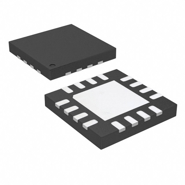
DC/DC converter in a tiny 3mm × 3mm package. The
1.2MHz/2.4MHz switching frequencies minimize the
solution footprint while maintaining high efficiency. Both
converters feature soft-start and internal compensation,
simplifying the design.
n
n
n
n
n
n
n
n
n
n
Dual High Efficiency DC/DC Converters:
Step-Up (VOUT = 1.8V to 5.25V, ISW = 600mA)
Step-Down (VOUT = 0.615V to 5.5V, IOUT = 400mA)
1.8V to 5.5V Input Voltage Range
Up to 94% Efficiency
Pin Selectable Burst Mode® Operation
45μA Quiescent Current in Burst Mode Operation
1.2MHz (LTC3523) or 2.4MHz (LTC3523-2)
Switching Frequency
Independent Power Good Indicator Outputs
Integrated Soft-Start
Thermal and Overcurrent Protection
VOUT OPERATION
The LTC3523/LTC3523-2 step-up converters will maintain
voltage regulation when the input voltage is above the
output voltage. Since this mode will dissipate more power,
the maximum output current is limited in order to maintain
an acceptable junction temperature and is given by:
IOUT(MAX ) =
250 – TA
T
136 • ⎡⎣(VIN + 1.5) – VOUT ⎤⎦
where TA = ambient temperature.
For example, at VIN = 4.5V, VOUT = 3.3V and TA = 85°C, the
maximum output current is limited to 449mA.
SHORT-CIRCUIT PROTECTION
The LTC3523/LTC3523-2’s step-up output disconnect
feature allows output short circuit while maintaining
a maximum internally set current limit. However, the
LTC3523/LTC3523-2 also incorporate internal features
such as current limit foldback and thermal shutdown for
protection from an excessive overload or short circuit.
During a prolonged short circuit of VOUT less than 950mV,
the current limit folds back to 2/3 the normal current limit.
This 2/3 current limit remains in effect until VOUT exceeds
1V, at which time the normal internal set current limit is
restored.
When the LTC3523/LTC3523-2 step-down converters output is shorted to ground, the step-down uses a comparator
to limit the current through the synchronous rectifying
N-channel switch to 650mA. If this limit is exceeded, the
P-channel switch is inhibited from turning on until the
current through the synchronous rectifying N-channel
switch falls below 650mA.
THERMAL CONSIDERATIONS
To deliver the LTC3523/LTC3523-2’s full-rated power, it is
imperative that a good thermal path be provided to dissipate the heat generated within the package. This can be
accomplished by taking advantage of the large thermal pad
on the underside of the LTC3523/LTC3523-2. It is recommended that multiple vias in the printed circuit board be
used to conduct heat away from the LTC3523/LTC3523-2
and into the copper plane with as much area as possible.
In the event that the junction temperature gets too high,
the LTC3523/LTC3523-2 will go into thermal shutdown
and all switching will cease until the internal temperature
drops to a safe level at which point the soft-start cycle
will be initiated.
3523fb
11
�LTC3523/LTC3523-2
APPLICATIONS INFORMATION
DUAL BUCK-BOOST AND STEP-UP CONVERTER
OPERATION
into the step-down’s SHDN2 pin. Note that the overall
3.3V converter efficiency is the product of the individual
efficiencies.
The LTC3523/LTC3523-2 can be operated in a cascaded
configuration as shown in Figure 2, allowing buck-boost
and step-up converter operation. Supply rail sequencing
is achieved by feeding the step-up converter PGOOD1
VIN
1.8V TO 5.25V
4.7μF
10μH
VIN1
VOUT1
STEP-UP
OUTPUT
5V
100mA
VBAT
VIN2
4.7μH
SW1
SW2
VOUT
FB2
10pF
10μF
768k
LTC3523
FB1
PGOOD1
10μF
182k
PGOOD2
SHDN2
SHDN1
243k
VIN
MODE
825k
VOUT2
STEP-DOWN
OUTPUT
3.3V
50mA
GND1 GND2 GND3
100k
VIN
3523 F02a
OFF ON
100
5V OUTPUT
90
EFFICIENCY (%)
80
70
3.3V OUTPUT
60
50
40
30
VIN = 2.4V
VOUT1 = 5V
VOUT2 = 3.3V
fOSC = 1.2MHz
BURST ENABLED
20
10
0
0.1
10
1
100
OUTPUT CURRENT (mA)
1000
3523 F02b
Figure 2. Dual Converter Efficiency (Load Applied
to Step-Down Output)
3523fb
12
�LTC3523/LTC3523-2
TYPICAL APPLICATIONS
Power Sequence Operation
VIN
1.8V TO 3.2V
2-CELL
ALKALINE
+
4.7μF
4.7μH
VIN1
VOUT1
STEP-UP
OUTPUT
3.3V
200mA
VIN2
VBAT
4.7μH
SW1
SW2
VOUT
FB2
10pF
4.7μF
634k
FB1
PGOOD1
365k
LTC3523
MODE
511k
10μF
VOUT2
STEP-DOWN
OUTPUT
1.2V
200mA
511k
PGOOD2
SHDN1
SHDN2
GND1 GND2 GND3
100k
VIN
OFF ON
3523 TA02a
VOUT1
2V/DIV
PGOOD2
VOUT2
1V/DIV
SHDN2
500μs/DIV
3523 TA02b
3523fb
13
�LTC3523/LTC3523-2
TYPICAL APPLICATIONS
Li-Ion to 5V/150mA, 2.5V/200mA
VIN
2.5V TO 4.2V
Li-Ion
+
4.7μF
10μH
VIN1
VOUT1
STEP-UP
OUTPUT
5V
150mA
VIN2
VBAT
4.7μH
SW1
SW2
VOUT
FB2
10pF
10μF
FB1
768k
PGOOD1
SHDN1
243k
LTC3523
MODE
VIN
768k
10μF
VOUT2
STEP-DOWN
OUTPUT
2.5V
200mA
243k
PGOOD2
SHDN2
GND1 GND2 GND3
OFF ON
OFF ON
3523 TA03
Efficiency and Power Loss
vs Load Current
1000
100
EFFICIENCY
90
100
70
60
P0WER
LOSS
50
40
10
VIN = 3.6V
VOUT1 = 5V
VOUT2 = 2.5V
fOSC = 1.2MHz
30
20
POWER LOSS (mW)
EFFICIENCY (%)
80
1
STEP-UP
STEP-DOWN
10
0
0
10
1
100
LOAD CURRENT (mA)
0
1000
3523 TA03b
3523fb
14
�LTC3523/LTC3523-2
PACKAGE DESCRIPTION
UD Package
16-Lead Plastic QFN (3mm × 3mm)
(Reference LTC DWG # 05-08-1691)
0.70 p0.05
3.50 p 0.05
1.45 p 0.05
2.10 p 0.05 (4 SIDES)
PACKAGE OUTLINE
0.25 p0.05
0.50 BSC
RECOMMENDED SOLDER PAD PITCH AND DIMENSIONS
3.00 p 0.10
(4 SIDES)
BOTTOM VIEW—EXPOSED PAD
PIN 1 NOTCH R = 0.20 TYP
OR 0.25 s 45o CHAMFER
R = 0.115
TYP
0.75 p 0.05
15
16
PIN 1
TOP MARK
(NOTE 6)
0.40 p 0.10
1
1.45 p 0.10
(4-SIDES)
2
(UD16) QFN 0904
0.200 REF
0.00 – 0.05
NOTE:
1. DRAWING CONFORMS TO JEDEC PACKAGE OUTLINE MO-220 VARIATION (WEED-2)
2. DRAWING NOT TO SCALE
3. ALL DIMENSIONS ARE IN MILLIMETERS
4. DIMENSIONS OF EXPOSED PAD ON BOTTOM OF PACKAGE DO NOT INCLUDE
MOLD FLASH. MOLD FLASH, IF PRESENT, SHALL NOT EXCEED 0.15mm ON ANY SIDE
5. EXPOSED PAD SHALL BE SOLDER PLATED
6. SHADED AREA IS ONLY A REFERENCE FOR PIN 1 LOCATION
ON THE TOP AND BOTTOM OF PACKAGE
0.25 p 0.05
0.50 BSC
3523fb
Information furnished by Linear Technology Corporation is believed to be accurate and reliable.
However, no responsibility is assumed for its use. Linear Technology Corporation makes no representation that the interconnection of its circuits as described herein will not infringe on existing patent rights.
15
�LTC3523/LTC3523-2
RELATED PARTS
PART NUMBER
DESCRIPTION
COMMENTS
LTC3400/LTC3400B
600mA (ISW), 1.2MHz, Synchronous Step-Up DC/DC Converters
92% Efficiency, VIN: 0.85V to 5V, VOUT(MAX) = 5V,
IQ = 19μA/300μA, ISD < 1μA, ThinSOTTM Package
LTC3401
1A (ISW), 3MHz, Synchronous Step-Up DC/DC Converter
97% Efficiency, VIN: 0.85V to 5V, VOUT(MAX) = 5.5V,
IQ = 38μA, ISD < 1μA, 10-Pin MS Package
LTC3402
2A (ISW), 3MHz, Synchronous Step-Up DC/DC Converter
97% Efficiency, VIN: 0.85V to 5V, VOUT(MAX) = 5.5V,
IQ = 38μA, ISD < 1μA, 10-Pin MS Package
LTC3421
3A (ISW), 3MHz, Synchronous Step-Up DC/DC Converter
with Output Disconnect Converter
94% Efficiency, VIN: 0.85V to 4.5V, VOUT(MAX) = 5.25V,
IQ = 12μA, ISD < 1μA, 24-Pin (4mm × 4mm) QFN Package
LTC3422
1.5A (ISW), 3MHz, Synchronous Step-Up DC/DC with Output
Disconnect Converter
94% Efficiency, VIN: 0.85V to 4.5V, VOUT(MAX) = 5.25V,
IQ = 25μA, ISD < 1μA, 10-Pin (3mm × 3mm) DFN Package
LTC3426
2A (ISW), 1.5MHz, Step-Up DC/DC Converter
92% Efficiency, VIN: 1.6V to 5.5V, VOUT(MAX) = 5V,
IQ = 600μA, ISD < 1μA, ThinSOT Package
LTC3427
500mA (ISW), 1.25MHz, Synchronous Step-Up DC/DC with Output
Disconnect Converter
94% Efficiency, VIN: 1.8V to 5V, VOUT(MAX) = 5.25V,
IQ = 350μA, ISD < 1μA, 6-Pin (2mm × 2mm) DFN Package
LTC3429/LTC3429B
600mA (ISW), 550kHz, Synchronous Step-Up DC/DC Converters
Soft-Start/Output Disconnect
96% Efficiency, VIN: 0.85V to 4.3V, VOUT(MAX) = 5V,
IQ = 20μA, ISD < 1μA, ThinSOT Package
LTC3459
80mA (ISW), Synchronous Step-Up DC/DC Converter
92% Efficiency, VIN: 1.5V to 5.5V, VOUT(MAX) = 10V,
IQ = 10μA, ISD < 1μA, ThinSOT Package
LTC3525-3
LTC3525-3.3
LTC3525-5
400mA (ISW), Synchronous Step-Up DC/DC Converters with Output 94% Efficiency, VIN: 0.85V to 4V, VOUT(MAX) = 5V,
Disconnect
IQ = 7μA, ISD < 1μA, SC-70 Package
LTC3526/LTC3526L
LTC3526B
500mA (ISW), 1MHz Synchronous Step-Up DC/DC Converters with
Output Disconnect
94% Efficiency, VIN: 0.85V to 5V, VOUT(MAX) = 5.25V,
IQ = 9μA, ISD < 1μA, 6-Pin (2mm × 2mm) DFN Package
LTC3528/LTC3528B
1A (ISW), 1MHz Synchronous Step-Up DC/DC Converters with
Output Disconnect
94% Efficiency, VIN: 0.85V to 5V, VOUT(MAX) = 5.25V,
IQ = 10μA, ISD < 1μA, 8-Pin (2mm × 3mm) DFN Package
ThinSOT is a trademark of Linear Technology Corporation.
3523fb
16 Linear Technology Corporation
LT 1108 REV B • PRINTED IN USA
1630 McCarthy Blvd., Milpitas, CA 95035-7417
(408) 432-1900 ● FAX: (408) 434-0507
●
www.linear.com
© LINEAR TECHNOLOGY CORPORATION 2008
�