LTC3545/LTC3545-1
Triple 800mA Synchronous
Step-Down Regulator–2.25MHz
FEATURES
■
■
■
■
■
■
■
■
■
■
DESCRIPTION
Three 800mA Outputs
High Efficiency: Up to 95%
2.25V to 5.5V Input Voltage Range
Low Ripple (1μF) supply bypass capacitors. The
discharged bypass capacitors are effectively put in parallel with COUT, causing a rapid drop in VOUT. No regulator
can deliver enough current to prevent this problem if the
load switch resistance is low and it is driven quickly. The
only solution is to limit the rise time of the switch drive
so that the load rise time is limited to approximately (25
• CLOAD). Thus, a 10μF capacitor charging to 3.3V would
require a 250μs rise time, limiting the charging current
to about 130mA.
Design Example
As a design example, consider using the LTC3545/LTC35451 in a portable application with a Li-Ion battery. The battery
provides VIN ranging from 2.8V to 4.2V. The demand on
one channel at 2.5V is 600mA. Using this channel as an
example, first calculate the inductor value for 40% ripple
current (240mA in this example) at maximum VIN. Using
a form of Equation 1:
L1=
2.5V
⎛ 2.5V ⎞
1–
= 1.41µH
(2.25MHz )(240mA ) ⎜⎝ 3.6V ⎟⎠
Use the closest standard value of 1.5μH. For low ripple
applications, 10μF is a good choice for the output capacitor.
A smaller output capacitor will shorten transient response
settling time, but also increase the load transient ripple. A
value for C5 = 4.7μF should suffice as the source impedance of a Li-Ion battery is very low. C5 and C1 both provide
switching current to the output power switches. They
should be placed as close a possible to the chip between
VIN/GNDA and PVIN/PGND respectively. PVIN and PGND
are the supply and return power paths for both channels
2 and 3, so a value of 10μF for C1 is appropriate. The
feedback resistors program the output voltage. Minimizing the current in these resistors will maximize efficiency
at very light loads, but totals on the order of 200k are a
good compromise between efficiency and immunity to
any adverse effects of PCB parasitic capacitance on the
feedback pins. Choosing 10μA as the feedback current with
0.6V feedback voltage makes R4 = 60k. A close standard
1% resistor is 60.4k. Using:
⎛ 2.5V ⎞
R3 = ⎜
– 1 • R4 = 191.1k
⎝ 0.6 V ⎟⎠
The closest standard 1% resistor is 191k. A 20pF feedforward capacitor is recommended to improve transient
response. The component values for the other channels
are chosen in a similar fashion. Figure 4 shows the complete schematic for this example, along with the efficiency
curve and burst mode ripple at an output current for the
2.5V output.
35451fb
15
�LTC3545/LTC3545-1
APPLICATIONS INFORMATION
PC Board Layout Checklist
When laying out the printed circuit board, the following
checklist should be used to ensure proper operation of
the LTC3545/LTC3545-1. These items are also illustrated
graphically in Figures 3 and 4. Figure 3 shows the power
path components and traces. In this figure the feedback
networks are not shown since they reside on the bottom
side of the board. Check the following in your layout:
1. The power traces consisting of the PGND trace, the SW
trace, the PVIN trace, the VIN and GNDA traces, should
be kept short direct and wide.
2. Does each of the VFBx pins connect directly to the
respective feedback resistors? The resistive dividers
must be connected between the (+) plate of the cor-
responding output filter capacitor (e.g. C2) and GNDA.
If the circuit being powered is at such a distance from
the part where voltage drops along circuit traces are
large, consider a Kelvin connection from the powered
circuit back to the resistive dividers.
3. Keep C1 and C5 as close to the part as possible.
4. Keep the switching nodes (SWx) away from the sensitive VFBx nodes.
5. Keep the ground connected plates of the input and
output capacitors as close as possible.
6. Care should be taken to provide enough space between
unshielded inductors in order to minimize any transformer coupling.
VOUT3
(VIA TO FEEDBACK
NETWORK)
L3
C4
SW3
VIN
C1
PVIN
PGND
C5
GNDA
SW1
SW2
C3
C2
L1
L2
VOUT2
(VIA TO FEEDBACK
NETWORK)
3545 F03
(VIA TO FEEDBACK
NETWORK)
VOUT1
Figure 3. Layout Diagram
35451fb
16
�LTC3545/LTC3545-1
TYPICAL APPLICATIONS
L1
1.5μH
C6
20pF
R2
511k
E2
PGOOD2
C5
4.7μF
R1
511k
1
2
E1
PGOOD1
3
4
5
6
7
VIN
2.7V TO 5.5V
C1
10μF
10V
8
SW1
LTC3545
PGOOD1
GNDA
VIN
RUN2
RUN1
PGOOD2
VFB1
SW2
VFB2
PGND
VFB3
PVIN
RUN3
SW3
SYNC/MODE
R3
191k
E3
VOUT1
C2
10μF
6.3V
2.5V AT 0.8A
E4
GND
R4
60.4k
16
15
14
L2
1.5μH
13
12
C7
20pF
11
R5
100k
10
E7
VOUT2
C3
10μF
6.3V
1.2V AT 0.8A
E6
GND
R6
100k
9
GND
L3
1.5μH
17
C8
20pF
R7
165k
E5
VOUT3
C4
10μF
6.3V
1.5V AT 0.8A
E8
GND
R8
110k
3545 TA02
Overall Efficiency vs
Channel 1 Load Current
Burst Mode Ripple
100
VOUT3
AC COUPLED
20mV/DIV
OVERALL EFFICIENCY (%)
90
80
70
IL3
250mA/DIV
60
50
40
30
20
10
0
0.1
SW3
2V/DIV
TA = 25°C
VIN = 3.6V
VOUT = 2.5V
fOSC = 2.25MHz
CHANNEL 2 = 1.2V, ILOAD = 400mA
CHANNEL 3 = 1.5V, ILOAD = 400mA
1
10
100
CHANNEL 1 LOAD CURRENT (mA)
1000
TA = 25°C
VIN = 3.6V
VOUT = 1.5V
ILOAD = 50mA
fOSC = 2.25MHz
1μs/DIV
3545 TA04
3545 TA03
Figure 4. LTC3545 Low Ripple Burst Mode Operation
35451fb
17
�LTC3545/LTC3545-1
TYPICAL APPLICATIONS
L1
1.5μH
C6
20pF
R9
511k
E9
PGOOD3
E2
PGOOD2
R2
511k
R1
511k
1
2
E1
PGOOD1
3
4
5
6
VIN
2.5V TO 5.5V
7
C1
4.7μF
8
SW1
LTC3545-1 GNDA
PGOOD1
VIN
RUN1
RUN2
PGOOD2
VFB1
SW2
VFB2
PGND
VFB3
PVIN
RUN3
SW3
PGOOD3
C2
10μF
E3
VOUT1
1.2V AT 0.8A
E4
GND
R4
100k
C5
10μF
16
R3
100k
15
14
L2
1.5μH
13
12
C7
20pF
11
R5
165k
C3
10μF
10
R6
110k
9
E7
VOUT2
1.5V AT 0.8A
E6
GND
GND
L3
1.5μH
17
C8
20pF
R7
133k
C4
10μF
E5
VOUT3
1.8V AT 0.8A
E8
GND
R8
66.5k
3545 TA05
3-Channel Power Sequencing
RUN1
VOUT1
VOUT2
VOUT3
PGOOD3
TA = 25°C
VIN = 3.6V
400μs/DIV
3545 TA06
Figure 5. LTC3545-1 Three PGOODs and Power Sequencing
35451fb
18
�LTC3545/LTC3545-1
PACKAGE DESCRIPTION
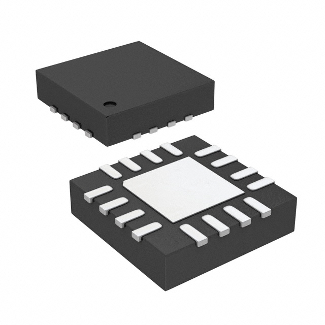
UD Package
16-Lead Plastic QFN (3mm s 3mm)
(Reference LTC DWG # 05-08-1700 Rev A)
Exposed Pad Variation AA
0.70 p0.05
3.50 p 0.05
1.65 p 0.05
2.10 p 0.05 (4 SIDES)
PACKAGE OUTLINE
0.25 p0.05
0.50 BSC
RECOMMENDED SOLDER PAD PITCH AND DIMENSIONS
3.00 p 0.10
(4 SIDES)
BOTTOM VIEW—EXPOSED PAD
PIN 1 NOTCH R = 0.20 TYP
OR 0.25 s 45o CHAMFER
R = 0.115
TYP
0.75 p 0.05
15
16
PIN 1
TOP MARK
(NOTE 6)
0.40 p 0.10
1
1.65 p 0.10
(4-SIDES)
2
(UD16 VAR A) QFN 1207 REV A
0.200 REF
0.00 – 0.05
NOTE:
1. DRAWING CONFORMS TO JEDEC PACKAGE OUTLINE MO-220 VARIATION (WEED-4)
2. DRAWING NOT TO SCALE
3. ALL DIMENSIONS ARE IN MILLIMETERS
4. DIMENSIONS OF EXPOSED PAD ON BOTTOM OF PACKAGE DO NOT INCLUDE
MOLD FLASH. MOLD FLASH, IF PRESENT, SHALL NOT EXCEED 0.15mm ON ANY SIDE
5. EXPOSED PAD SHALL BE SOLDER PLATED
6. SHADED AREA IS ONLY A REFERENCE FOR PIN 1 LOCATION
ON THE TOP AND BOTTOM OF PACKAGE
0.25 p 0.05
0.50 BSC
35451fb
Information furnished by Linear Technology Corporation is believed to be accurate and reliable.
However, no responsibility is assumed for its use. Linear Technology Corporation makes no representation that the interconnection of its circuits as described herein will not infringe on existing patent rights.
19
�LTC3545/LTC3545-1
RELATED PARTS
PART NUMBER
DESCRIPTION
COMMENTS
LTC3405/LTC3405A
300mA IOUT, 1.5MHz, Synchronous Step-Down DC/DC
Converters
95% Efficiency, VIN: 2.5V to 5.5V, VOUT(MIN) = 0.8V, IQ = 20μA,
ISD < 1μA, ThinSOT™ Package
LTC3406/LTC3406B
600mA IOUT, 1.5MHz, Synchronous Step-Down DC/DC
Converters
96% Efficiency, VIN: 2.5V to 5.5V, VOUT(MIN) = 0.6V, IQ = 20μA,
ISD < 1μA, ThinSOT Package
LTC3407/LTC3407-2
Dual 600mA/800mA IOUT, 1.5MHz/2.25MHz,
Synchronous Step-Down DC/DC Converters
95% Efficiency, VIN: 2.5V to 5.5V, VOUT(MIN) = 0.6V, IQ = 40μA,
ISD < 1μA, 10-Lead MSE, DFN Packages
LTC3409
600mA IOUT, 1.7MHz/2.6MHz, Synchronous Step-Down
DC/DC Converter
96% Efficiency, VIN: 1.6V to 5.5V, VOUT(MIN) = 0.6V, IQ = 65μA,
ISD < 1μA, DFN Package
LTC3410/LTC3410B
300mA IOUT, 2.25MHz, Synchronous Step-Down DC/DC
Converters
95% Efficiency, VIN: 2.5V to 5.5V, VOUT(MIN) = 0.8V, IQ = 26μA,
ISD < 1μA, SC70 Package
LTC3411
1.25A IOUT, 4MHz, Synchronous Step-Down DC/DC
Converter
95% Efficiency, VIN: 2.5V to 5.5V, VOUT(MIN) = 0.8V, IQ = 60μA,
ISD < 1μA, 10-Lead MSE, DFN Packages
LTC3412
2.5A IOUT, 4MHz, Synchronous Step-Down DC/DC
Converter
95% Efficiency, VIN: 2.5V to 5.5V, VOUT(MIN) = 0.8V, IQ = 60μA,
ISD < 1μA, 16-Lead TSSOPE Package
LTC3419
Dual 600mA, 2.25MHz, Synchronous Step-Down DC/DC 96% Efficiency, VIN: 2.5V to 5.5V, VOUT(MIN) = 0.6V, IQ = 35μA,
ISD < 1μA, MS10, 3mm × 3mm DFN Package
Converter
LTC3441/LTC3442
LTC3443
1.2A IOUT, 2MHz, Synchronous Buck-Boost DC/DC
Converters
95% Efficiency, VIN: 2.4V to 5.5V, VOUT(MIN): 2.4V to 5.25V, IQ = 50μA,
ISD < 1μA, DFN Package
LTC3531/LTC3531-3
LTC3531-3.3
200mA IOUT, 1.5MHz, Synchronous Buck-Boost DC/DC
Converters
95% Efficiency, VIN: 1.8V to 5.5V, VOUT(MIN): 2V to 5V, IQ = 16μA,
ISD < 1μA, ThinSOT, DFN Packages
LTC3532
500mA IOUT, 2MHz, Synchronous Buck-Boost DC/DC
Converter
95% Efficiency, VIN: 2.4V to 5.5V, VOUT(MIN): 2.4V to 5.25V, IQ = 35μA,
ISD < 1μA, 10-Lead MSE, DFN Packages
LTC3544/LTC3544B
300mA, 2 × 200mA, 100mA, 2.25MHz Quad
Synchronous Step-Down DC/DC Converter
95% Efficiency, VIN: 2.5V to 5.5V, VOUT(MIN) = 0.8V, IQ = 60μA,
ISD < 1μA, 3mm × 3mm QFN Package
LTC3547
Dual 300mA IOUT, 2.25MHz, Synchronous Step-Down
DC/DC Converter
95% Efficiency, VIN: 2.5V to 5.5V, VOUT(MIN) = 0.6V, IQ = 40μA,
ISD < 1μA, 8-Lead DFN Package
LTC3548/LTC3548-1
LTC3548-2
Dual 400mA/800mA IOUT, 2.25MHz, Synchronous
Step-Down DC/DC Converters
95% Efficiency, VIN: 2.5V to 5.5V, VOUT(MIN) = 0.6V, IQ = 40μA,
ISD < 1μA, 10-Lead MSE, DFN Packages
LTC3561
1.25A IOUT, 4MHz, Synchronous Step-Down DC/DC
Converter
95% Efficiency, VIN: 2.5V to 5.5V, VOUT(MIN) = 0.8V, IQ = 240μA,
ISD < 1μA, DFN Package
ThinSOT is a Trademark of Linear Technology Corporation.
35451fb
20 Linear Technology Corporation
LT 0908 REV B • PRINTED IN USA
1630 McCarthy Blvd., Milpitas, CA 95035-7417
(408) 432-1900
●
FAX: (408) 434-0507 ● www.linear.com
© LINEAR TECHNOLOGY CORPORATION 2008
�


 工商网监
湘ICP备2023018690号
工商网监
湘ICP备2023018690号

