Features
Programmable Average Input Current Limit:
±5% Accuracy
n Dual Step-Down Outputs: Up to 96% Efficiency
n Low Noise Pulse-Skipping Operation at Light Loads
n Input Voltage Range: 2.5V to 5.5V
n Output Voltage Range: 0.6V to 5V
n 2.25MHz Constant-Frequency Operation
n Power Good Output Voltage Monitor for Each Channel
n Low Dropout Operation: 100% Duty Cycle
n Independent Internal Soft-Start for Each Channel
n Current Mode Operation for Excellent Line and Load
Transient Response
n ±2% Output Voltage Accuracy
n Short-Circuit Protected
n Shutdown Current ≤ 1μA
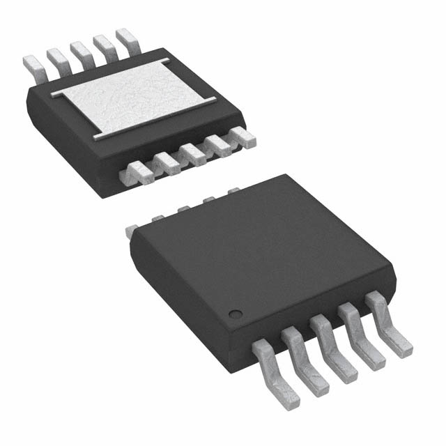
n Available in Small Thermally Enhanced 10-Lead MS
and 3mm × 3mm DFN Packages
n
Applications
n
n
n
n
High Peak Load Current Applications
USB Powered Devices
Supercapacitor Charging
Radio Transmitters and Other Handheld Devices
L, LT, LTC, LTM, Linear Technology, the Linear logo and Burst Mode are registered trademarks
and Hot Swap is a trademark of Linear Technology Corporation. All other trademarks are the
property of their respective owners. Protected by U.S. Patents, including 5481178, 6127815,
6304066, 6498466, 6580258, 6611131.
LTC3619B
400mA/800mA Synchronous
Step-Down DC/DC with
Average Input Current Limit
Description
The LTC®3619B is a dual monolithic synchronous buck
regulator using a constant frequency current mode architecture.
The input supply voltage range is 2.5V to 5.5V, making it
ideal for Li-Ion and USB powered applications. 100% duty
cycle capability provides low dropout operation, extending the run time in battery-operated systems. Low output
voltages are supported with the 0.6V feedback reference
voltage. Channel 1 and channel 2 can supply 400mA and
800mA output current, respectively.
The LTC3619B’s programmable average input current limit
is ideal for USB applications and for point-of-load power
supplies because the LTC3619B’s limited input current
will still allow its output to deliver high peak load currents
without collapsing the input supply. When the sum of
both channels’ currents exceeds the input current limit,
channel 2 is current limited while channel 1 remains regulated. The operating frequency is internally set at 2.25MHz
allowing the use of small surface mount inductors. Internal
soft-start reduces in-rush current during start-up. The
LTC3619B is available in small MSOP and 3mm × 3mm
DFN packages. The LTC3619B is also available in a low
quiescent current, high efficiency Burst Mode® version,
LTC3619.
Typical Application
GSM Pulse Load
Dual Monolithic Buck Regulator in 10-Lead 3mm × 3mm DFN
VIN
3.4V TO 5.5V
10µF
VOUT
200mV/DIV
RUN2 VIN RUN1
PGOOD2 PGOOD1
1.5µH
VOUT2
3.4V AT
800mA
LTC3619B
SW2
+
1190k
2.2mF
×2
SuperCap
SW1
22pF
VFB1
VFB2
255k
3.3µH
RLIM GND
255k
511k
VOUT1
1.8V AT
400mA
10µF
VIN
AC-COUPLED
1V/DIV
IOUT
500mA/DIV
IIN
500mA/DIV
1ms/DIV
3619B TA01
1000pF
116k
3619B TA01b
VIN = 5V, 500mA COMPLIANT
ILOAD = 0A to 2.2A, CHANNEL 1 UNLOADED
ILIM = 475mA
3619bfb
1
�LTC3619B
Absolute Maximum Ratings
(Note 1)
Input Supply Voltage (VIN).............................. –0.3 to 6V
VFB1, VFB2......................................... –0.3V to VIN + 0.3V
RUN1, RUN2, RLIM........................... –0.3V to VIN + 0.3V
SW1, SW2......................................... –0.3V to VIN + 0.3V
PGOOD1, PGOOD2............................ –0.3V to VIN + 0.3V
P-channel SW Source Current (DC) (Note 2)
Channel 1......................................................... 600mA
Channel 2.................................................................1A
N-channel SW Source Current (DC) (Note 2)
Channel 1......................................................... 600mA
Channel 2.................................................................1A
Peak SW Source and Sink Current (Note 2)
Channel 1......................................................... 900mA
Channel 2.............................................................. 2.7A
Operating Junction Temperature Range
(Notes 3, 6, 8).........................................–40 to 125°C
Storage Temperature Range................... –65°C to 125°C
Lead Temperature (Soldering, 10 sec)
MSOP Package.................................................. 300°C
Reflow Peak Body Temperature............................. 260°C
Pin Configuration
TOP VIEW
VFB1
1
RUN1
2
RLIM
3
PGOOD1
4
SW1
5
TOP VIEW
10 VFB2
11
GND
VFB1
RUN1
RLIM
PGOOD1
SW1
9 RUN2
8 PGOOD2
7 SW2
6 VIN
1
2
3
4
5
11
GND
10
9
8
7
6
VFB2
RUN2
PGOOD2
SW2
VIN
MSE PACKAGE
10-LEAD PLASTIC MSOP
TJMAX = 125°C, θJA = 45°C/W
EXPOSED PAD (PIN 11) IS GND, MUST BE SOLDERED TO PCB
DD PACKAGE
10-LEAD (3mm × 3mm) PLASTIC DFN
TJMAX = 125°C, θJA = 40°C/W
EXPOSED PAD (PIN 11) IS GND, MUST BE SOLDERED TO PCB
Order Information
LEAD FREE FINISH
TAPE AND REEL
PART MARKING*
PACKAGE DESCRIPTION
TEMPERATURE RANGE
LTC3619BEDD#PBF
LTC3619BEDD#TRPBF
LFFH
10-Lead (3mm × 3mm) Plastic DFN
–40°C to 125°C
LTC3619BIDD#PBF
LTC3619BIDD#TRPBF
LFFH
10-Lead (3mm × 3mm) Plastic DFN
–40°C to 125°C
LTC3619BEMSE#PBF
LTC3619BEMSE#TRPBF
LTFFJ
10-Lead Plastic MSOP
–40°C to 125°C
LTC3619BIMSE#PBF
LTC3619BIMSE#TRPBF
LTFFJ
10-Lead Plastic MSOP
–40°C to 125°C
Consult LTC Marketing for parts specified with wider operating temperature ranges. *The temperature grade is identified by a label on the shipping container.
Consult LTC Marketing for information on non-standard lead based finish parts.
For more information on lead free part marking, go to: http://www.linear.com/leadfree/
For more information on tape and reel specifications, go to: http://www.linear.com/tapeandreel/
Electrical Characteristics
The l denotes the specifications which apply over the full operating
junction temperature range, otherwise specifications are at TA = 25°C (Note 3)
SYMBOL
PARAMETER
VIN
VIN Operating Voltage Range
VUV
VIN Undervoltage Lockout
CONDITIONS
MIN
l
VIN Low to High
l
TYP
2.5
2.1
MAX
UNITS
5.5
V
2.5
V
3619bfb
2
�LTC3619B
Electrical
Characteristics
The l denotes the specifications which apply over the full operating
junction temperature range, otherwise specifications are at TA = 25°C (Note 3)
SYMBOL
PARAMETER
IFB
Feedback Pin Input Current
MAX
UNITS
±30
nA
VFBREG
Feedback Voltage (Channels 1, 2)
LTC3619BE, –40°C < TJ < 85°C (Note 7)
LTC3619BI, –40°C < TJ < 125°C (Note 7)
0.600
0.600
0.612
0.618
V
V
ΔVLINEREG
VFB Line Regulation
VIN = 2.5V to 5.5V (Note 7)
0.01
0.25
%/V
ΔVLOADREG
VFB Load Regulation (Channel 1)
VFB Load Regulation (Channel 2)
ILOAD = 0mA to 400mA (Note 7)
ILOAD = 0mA to 800mA (Note 7)
0.5
0.5
IS
Supply Current
Active Mode (Note 4)
Shutdown
VFB1 = VFB2 = 0.95 × VFBREG
VRUN1 = VRUN2 = 0V, VIN = 5.5V
600
875
1
µA
µA
fOSC
Oscillator Frequency
VFB = VFBREG
1.8
2.25
2.7
MHz
ILIM(PEAK)
Peak Switch Current Limit
Channel 1 (400mA)
Channel 2 (800mA)
VIN = 5V, VFB < VFBREG , Duty Cycle 100pF at the RLIM pin.
Each application input current limit will call for different
CLIM value to optimize its response time. Using a large CLIM
capacitor requires longer time for the RLIM pin voltage
to charge. For example, consider the application 500mA
input current limit, 5V input and 1A, 2.5V output with a
50% duty cycle. When an instantaneous 1A output pulse is
applied, the current out of the RLIM pin becomes 1A/55k
= 18.2µA during the 50% on-time or 9.1µA full duty cycle.
With a CLIM capacitor of 1µF, RLIM of 116k, and using I =
CdV/dt, it will take 110ms for CLIM to charge from 0V to
1V. This is the time after which the LTC3619B will start
input current limiting. Any current within this time must be
considered in each application to determine if it is tolerable.
3619bfb
9
�LTC3619B
Operation
Figure 1a shows VIN (IIN) current below input current limit
with a CLIM capacitor of 0.1µF. Channel 1 is unloaded to
simplify calculations. When the load pulse is applied,
under the specified condition, ILIM current is 1.1A/55k •
0.66 = 13.2µA, where 0.66 is the duty cycle. It will take a
little more than 7.5ms to charge the CLIM capacitor from
0V to 1V, after which the LTC3619B begins to limit input
current. The IIN current is not limited during this 7.5ms
time and is more than 725mA. This current transient may
cause the input supply to temporarily droop if the supply
current compliance is exceeded, but recovers after the
input current limit engages. The output will continue to
deliver the required current load while the output voltage
droops to allow the input voltage to remain regulated
during input current limit.
this 92µs, the input current limit is not yet engaged and
the output must deliver the required current load. This
may cause the input voltage to droop if the current compliance is exceeded. Depending on how long this time is,
the VIN supply decoupling capacitor can provide some of
this current before VIN droops too much. In applications
with a bigger VIN supply decoupling capacitor and where
VIN supply is allow to droop closer to dropout, the CLIM
capacitor can be increased slightly. This will delay the
start of input current limit and artificially regulated VOUT
before input current limit is engaged. In this case, within
the 577µs load pulse, the VOUT voltage will stay artificially
regulated for 92µs out of the total 577µs before the input
current limit activates. This approach may be used if a
faster recovery on the output is desired.
For applications with short load pulse duration, a smaller
CLIM capacitor may be the better choice as in the example
shown in Figure 1b. Channel 1 is unloaded for simplification. In this example, a 577µs, 0A to 2A output pulse
is applied once every 4.7ms. A CLIM capacitor of 2.2nF
requires 92µs for VRLIM to charge from 0V to 1V. During
Selecting a very small CLIM will speed up response time
but it can put the device within threshold of interfering
with normal operation and input current limit in every
few switching cycles. This may be undesirable in terms
of noise. Use 2πRC >> 100/clock frequency (2.25MHz) as
a starting point, R being RLIM, C being CLIM.
VOUT
2V/DIV
VOUT
200mV/DIV
IIN
500mA/DIV
VIN
AC-COUPLED
1V/DIV
VRLIM
1V/DIV
IOUT
500mA/DIV
IIN
500mA/DIV
IL
1A/DIV
50ms/DIV
3619B F01a
VIN = 5V, 500mA COMPLIANT
RLIM = 116k, CLIM = 0.1µF
ILOAD = 0A to 1.1A, COUT = 2.2mF, VOUT = 3.3V
ILIM = 475mA, CHANNEL 1 NOT LOADED
Figure 1a. Input Current Limit Within 100ms Load Pulses
1ms/DIV
3619B F01b
VIN = 5V, 500mA COMPLIANT
RLIM = 116k, CLIM = 2200pF
ILOAD = 0A to 2A, COUT = 2.2mF, VOUT = 3.3V
ILIM = 475mA, CHANNEL 1 NOT LOADED
Figure 1b. Input Current Limit Within
577µs, 2A Repeating Load Pulses
3619bfb
10
�LTC3619B
Applications Information
A general LTC3619B application circuit is shown in Figure 2.
External component selection is driven by the load requirement, and begins with the selection of the inductor L. Once
the inductor is chosen, CIN and COUT can be selected.
Inductor Selection
Although the inductor does not influence the operating
frequency, the inductor value has a direct effect on ripple
current. The inductor ripple current DIL decreases with
higher inductance and increases with higher VIN or VOUT :
VOUT VOUT
• 1−
fO • L
VIN
ΔIL =
(1)
Accepting larger values of DIL allows the use of low
inductances, but results in higher output voltage ripple,
greater core losses, and lower output current capability.
A reasonable starting point for setting ripple current is
40% of the maximum output load current. So, for a 800mA
regulator, DIL = 320mA (40% of 800mA).
The inductor value will also have an effect on Burst Mode
operation. The transition to low current operation begins
when the peak inductor current falls below a level set by
the internal burst clamp. Lower inductor values result in
higher ripple current which causes the transition to occur
at lower load currents. This causes a dip in efficiency in
the upper range of low current operation. Furthermore,
lower inductance values will cause the bursts to occur
with increased frequency.
RUN2 VIN RUN1
L2
VOUT2
SW2
CF2
COUT2
R4
R3
SW1
VFB2
RLIM
CLIM
VFB1
GND
Table 1. Representative Surface Mount Inductors
MANUFACTURER
PART NUMBER
L1
CF1
R1
R2
RLIM
VOUT1
COUT1
3619B F02
MAX DC
VALUE CURRENT
DCR
HEIGHT
Coilcraft
LPS4012-152ML
LPS4012-222ML
LPS4012-332ML
LPS4012-472ML
LPS4018-222ML
LPS4018-332ML
LPS4018-472ML
1.5µH
2.2µH
3.3µH
4.7µH
2.2µH
3.3µH
4.7µH
2200mA
1750mA
1450mA
1450mA
2300mA
2000mA
1800mA
0.070Ω
0.100Ω
0.100Ω
0.170Ω
0.070Ω
0.080Ω
0.125Ω
1.2mm
1.2mm
1.2mm
1.2mm
1.8mm
1.8mm
1.8mm
FDK
FDKMIPF2520D
FDKMIPF2520D
FDKMIPF2520D
4.7µH
3.3µH
2.2µH
1100mA
1200mA
1300mA
0.11Ω
0.1Ω
0.08Ω
1mm
1mm
1mm
LQH32CN4R7M23 4.7µH
450mA
0.2Ω
2mm
ELT5KT4R7M
4.7µH
950mA
0.2Ω
1.2mm
CDRH2D18/LD
CDH38D11SNP3R3M
CDH38D11SNP2R2M
4.7µH
3.3μH
630mA
1560mA
0.086Ω
0.115Ω
2mm
1.2mm
2.2μH
1900mA
0.082Ω
1.2mm
2.2µH
2.2µH
3.3µH
2.2µH
4.7µH
510mA
530mA
410mA
1100mA
750mA
0.13Ω
0.33Ω
0.27Ω
0.1Ω
0.19Ω
1.6mm
1.25mm
1.6mm
1mm
1mm
4.7µH
700mA
0.28Ω
1mm
3.3µH
870mA
0.17Ω
1mm
2.2µH
1000mA
0.12Ω
1mm
2.2µH
1500mA
0.076Ω
1.2mm
3.3μH
1700mA
0.095Ω
1.2mm
2.2µH
2300mA
0.059Ω
1.4mm
Murata
Panasonic
Sumida
TDK
PGOOD2 PGOOD1
LTC3619B
Different core materials and shapes will change the size/
current and price/current relationship of an inductor. Toroid or shielded pot cores in ferrite or permalloy materials
are small and do not radiate much energy, but generally
cost more than powdered iron core inductors with similar
electrical characteristics. The choice of which style inductor to use often depends more on the price versus size
requirements, and any radiated field/EMI requirements,
than on what the LTC3619B requires to operate. Table 1
shows some typical surface mount inductors that work
well in LTC3619B applications.
Taiyo Yuden CB2016T2R2M
CB2012T2R2M
CB2016T3R3M
NR30102R2M
NR30104R7M
VIN
2.5V TO 5.5V
C1
Inductor Core Selection
VLF3010AT4R7MR70
VLF3010AT3R3MR87
VLF3010AT2R2M1R0
VLF4012AT-2R2
M1R5
VLF5012ST-3R3
M1R7
VLF5014ST-2R2
M2R3
Figure 2. LTC3619B General Schematic
3619bfb
11
�LTC3619B
Applications Information
Input Capacitor (CIN) Selection
In continuous mode, the input current of the converter is a
square wave with a duty cycle of approximately VOUT / VIN .
To prevent large voltage transients, a low equivalent series
resistance (ESR) input capacitor sized for the maximum
RMS current must be used. The maximum RMS capacitor
current is given by:
IRMS ≈IMAX
VOUT (VIN − VOUT )
VIN
Where the maximum average output current IMAX equals
the peak current minus half the peak-to-peak ripple current, IMAX = ILIM – DIL /2. This formula has a maximum at
VIN = 2VOUT, where IRMS = IOUT/2. This simple worst-case
is commonly used to design because even significant
deviations do not offer much relief. Note that capacitor
manufacturer’s ripple current ratings are often based on
only 2000 hours lifetime. This makes it advisable to further
derate the capacitor, or choose a capacitor rated at a higher
temperature than required. Several capacitors may also be
paralleled to meet the size or height requirements of the
design. An additional 0.1µF to 1µF ceramic capacitor is
also recommended on VIN for high frequency decoupling
when not using an all-ceramic capacitor solution.
Output Capacitor (COUT) Selection
The selection of COUT is driven by the required effective
series resistance (ESR). Typically, once the ESR requirement for COUT has been met, the RMS current rating
generally far exceeds the IRIPPLE(P-P) requirement. The
output ripple DVOUT is determined by:
1
ΔVOUT ≈ ΔIL ESR +
8fOCOUT
capacitor types include Sanyo POSCAP, Kemet T510 and
T495 series, and Sprague 593D and 595D series. Consult
the manufacturer for other specific recommendations.
Using Ceramic Input and Output Capacitors
Higher values, lower cost ceramic capacitors are now
becoming available in smaller case sizes. Their high ripple
current, high voltage rating and low ESR make them
ideal for switching regulator applications. Because the
LTC3619B control loop does not depend on the output
capacitor’s ESR for stable operation, ceramic capacitors
can be used freely to achieve very low output ripple and
small circuit size.
However, care must be taken when ceramic capacitors are
used at the input. When a ceramic capacitor is used at the
input and the power is supplied by a wall adapter through
long wires, a load step at the output can induce ringing at
the input, VIN. At best, this ringing can couple to the output
and be mistaken as loop instability. At worst, a sudden
inrush of current through the long wires can potentially
cause a voltage spike at VIN, large enough to damage the
part. For more information, see Application Note 88.
When choosing the input and output ceramic capacitors,
choose the X5R or X7R dielectric formulations. These
dielectrics have the best temperature and voltage characteristics of all the ceramics for a given value and size.
Setting the Output Voltage
The LTC3619B regulates the VFB1 and VFB2 pins to 0.6V
during regulation. Thus, the output voltage is set by a resistive divider, Figure 2, according to the following formula:
R2
VOUT = 0.6V 1+
R1
(2)
where fO = operating frequency, COUT = output capacitance
and DIL = ripple current in the inductor. For a fixed output
voltage, the output ripple is highest at maximum input
voltage since DIL increases with input voltage.
Keeping the current small (< 10µA) in these resistors
maximizes efficiency, but making it too small may allow
stray capacitance to cause noise problems or reduce the
phase margin of the error amp loop.
If tantalum capacitors are used, it is critical that the capacitors are surge tested for use in switching power supplies.
An excellent choice is the AVX TPS series of surface mount
tantalum. These are specially constructed and tested for low
ESR so they give the lowest ESR for a given volume. Other
To improve the frequency response of the main control
loop, a feedback capacitor (CF) may also be used. Great
care should be taken to route the VFB line away from noise
sources, such as the inductor or the SW line.
3619bfb
12
�LTC3619B
Applications Information
Checking Transient Response
The regulator loop response can be checked by looking
at the load transient response. Switching regulators take
several cycles to respond to a step in load current. When
a load step occurs, VOUT immediately shifts by an amount
equal to DILOAD • ESR, where ESR is the effective series
resistance of COUT. DILOAD also begins to charge or discharge COUT generating a feedback error signal used by the
regulator to return VOUT to its steady-state value. During
this recovery time, VOUT can be monitored for overshoot
or ringing that would indicate a stability problem.
The initial output voltage step may not be within the
bandwidth of the feedback loop, so the standard second
order overshoot/DC ratio cannot be used to determine the
phase margin. In addition, feedback capacitors (CF1 and
CF2) can be added to improve the high frequency response,
as shown in Figure 2. Capacitor CF provides phase lead by
creating a high frequency zero with R2 which improves
the phase margin.
The output voltage settling behavior is related to the stability
of the closed-loop system and will demonstrate the actual
overall supply performance. For a detailed explanation of
optimizing the compensation components, including a
review of control loop theory, refer to Application Note 76.
In some applications, a more severe transient can be caused
by switching in loads with large (>1µF) input capacitors.
The discharged input capacitors are effectively put in parallel with COUT, causing a rapid drop in VOUT. No regulator
can deliver enough current to prevent this problem if the
switch connecting the load has low resistance and is driven
quickly. The solution is to limit the turn-on speed of the
load switch driver. A Hot Swap™ controller is designed
specifically for this purpose and usually incorporates current limiting, short-circuit protection, and soft-starting.
Efficiency Considerations
The percent efficiency of a switching regulator is equal to
the output power divided by the input power times 100%.
It is often useful to analyze individual losses to determine
what is limiting the efficiency and which change would
produce the most improvement. Percent efficiency can
be expressed as:
% Efficiency = 100% – (L1 + L2 + L3 + ...)
where L1, L2, etc., are the individual losses as a percentage of input power.
Although all dissipative elements in the circuit produce
losses, four sources usually account for the losses in
LTC3619B circuits: 1) VIN quiescent current, 2) switching
losses, 3) I2R losses, 4) other system losses.
1. The VIN current is the DC supply current given in the
Electrical Characteristics which excludes MOSFET
driver and control currents. VIN current results in a
small (


 工商网监
湘ICP备2023018690号
工商网监
湘ICP备2023018690号
