LTC3773
Triple Output Synchronous
3-Phase DC/DC Controller with
Up/Down Tracking
FEATURES
■
■
■
■
■
■
■
■
■
■
■
DESCRIPTION
The LTC®3773 is a high performance, 3-phase, triple output
synchronous step-down switching regulator controller
with output voltage power up/down tracking capability.
The controller allows for sequential, coincident or ratiometric tracking.
Current Mode Controller with Onboard
MOSFET Drivers
Programmable Power Up/Down Tracking
Wide VIN Range: 3.3V to 36V (VCC = 5V)
±1% 0.6V VFB Accuracy Over Temperature
Power Good Output Voltage Monitor
Phase-Lockable or Adjustable Frequency:
160kHz to 700kHz
OPTI-LOOP® Compensation Minimizes COUT
Current Foldback and Overvoltage Protection
Selectable Continuous, Discontinuous or
Burst Mode® Operation at Light Load
Programmable Phase Operation
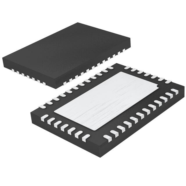
Available in 5mm x 7mm QFN and 36-Lead
SSOP Packages
This 3-phase controller drives its output stages with 120°
phase separation at frequencies of up to 700kHz per phase
minimizing the RMS input current. Light load efficiency can
be maximized by using selectable Burst Mode operation.
The 0.6V precision reference supports output voltages
from 0.6V to 5V.
Fault protection features include output overvoltage, input
undervoltage lockout plus current foldback under shortcircuit or overload conditions.
, LT, LTC, LTM, Burst Mode and OPTI-LOOP are registered trademarks of
Linear Technology Corporation. All other trademarks are the property of their respective
owners. Protected by U.S. Patents including 5408150, 5481178, 5705919, 5929620,
6144194, 6177787, 6304066, 6498466, 6580258, 6611131.
APPLICATIONS
■
■
■
Servers, Telecom, Industrial Power Supplies
General Purpose Multiple Rail DC/DC
FPGA and DSP Requirements
TYPICAL APPLICATION
High Efficiency, 3-Phase, Triple Synchronous DC/DC Step-Down Controller
VCC
4.5V TO 6V
10k
0.1μF
PGOOD VCC
POWER UP/SHUTDOWN
BOOST1, 2, 3
SDB1, 2, 3
VIN
2.2μH
VOUT2
0.003Ω 1.8V/15A
1.5μH
TG3
SW1
COUT2
SENSE2+
SENSE2–
VFB2
TG1
20k
VIN
VOUT3
0.003Ω 1.2V/15A
1.2μH
SW3
BG3
31.6k
10k
SENSE1+
SENSE1–
VFB1
ITH1, 2, 3
PLLFLTR
CIN
+
BG2
LTC3773
BG1
COUT1
VIN
4.5V TO 22V
VDR
TG2
SW2
TRACK1, 2, 3
0.01μF
VOUT1
2.5V/15A 0.003Ω
10μF
SW1, 2, 3
PGOOD
10k
COUT3
PGND
SGND
SENSE3+
SENSE3–
VFB3
3773 F01
20k
20k
3773fb
1
�LTC3773
ABSOLUTE MAXIMUM RATINGS
(Note 1)
Topside Driver Voltage (BOOSTn) .............. 42V to –0.3V
Switch Voltage (SWn) ................................... 36V to –1V
Boosted Driver Voltage (BOOSTn – SWn) .... 7V to –0.3V
Supply Voltages (VCC, VDR).......................... 7V to –0.3V
PGOOD, PHASEMD, PLLFLTR, PLLIN/FC, SDBn,
TRACKn, VFBn ...............................(VCC + 0.3V) to –0.3V
SENSE+n, SENSE –n ........................ (1.1 • VCC) to –0.3V
ITHn Voltage............................................... 2.7V to –0.3V
Extended Commercial Operating
Temperature Range (Note 2)................–40°C to 85°C
Junction Temperature (Note 2) ............................. 125°C
Storage Temperature Range...................–65°C to 125°C
Lead Temperature (Soldering, 10 sec)
G Package ......................................................... 300°C
Peak Body Temperature UHF Package................... 240°C
34 BOOST1
TRACK1
4
33 TG1
VFB1
5
32 SW1
ITH1
6
31 SW2
SGND
7
30 TG2
ITH2
8
29 BOOST2
ITH3
9
PGOOD
35 PGOOD
3
SENSE1+
2
SDB
SENSE1–
SENSE1–
SDB2
36 PHASEMD
SDB3
1
SDB1
TOP VIEW
TOP VIEW
SENSE1+
PHASEMD
PIN CONFIGURATIONS
38 37 36 35 34 33 32
31 BOOST1
TRACK1 1
VFB1 2
30 TG1
ITH1 3
29 SW1
SGND 4
28 SW2
27 TG2
28 BOOST3
ITH2 5
VFB2 10
27 TG3
ITH3 6
VFB3 11
26 SW3
VFB2 7
TRACK2 12
25 BG1
VFB3 8
24 TG3
TRACK3 13
24 BG2
TRACK2 9
23 SW3
23 VDR
22 PGND
TRACK3 10
22 BG1
SENSE2– 11
21 BG2
21 BG3
20 PLLIN/FC
BG3
19 PLLFLTR
G PACKAGE
36-LEAD PLASTIC SSOP
CLKOUT
VCC 18
20 VDR
13 14 15 16 17 18 19
PLLIN/FC
SENSE3+ 17
25 BOOST3
SENSE2+ 12
PLLFLTR
16
SENSE3 –
SENSE3
–
VCC
SENSE2+ 15
SENSE3+
SENSE2 – 14
26 BOOST2
39
UHF PACKAGE
38-LEAD (5mm × 7mm) PLASTIC QFN
EXPOSED PAD IS PGND (PIN 39),
MUST BE SOLDERED TO PCB
TJMAX = 125°C, θJA = 95°C/W
TJMAX = 125°C, θJA = 34°C/W
ORDERING INFORMATION
LEAD FREE FINISH
TAPE AND REEL
LTC3773EG#PBF
LTC3773EG#TRPBF
LTC3773EUHF#PBF
LTC3773EUHF#TRPBF
PART MARKING
3773E
PACKAGE DESCRIPTION
TEMPERATURE RANGE
36-Lead Plastic SSOP
–40°C to 85°C
38-Lead (5mm x 7mm) Plastic QFN
–40°C to 85°C
Consult LTC Marketing for parts specified with wider operating temperature ranges.
Consult LTC Marketing for information on non-standard lead based finish parts.
For more information on lead free part marking, go to: http://www.linear.com/leadfree/
For more information on tape and reel specifications, go to: http://www.linear.com/tapeandreel/
3773fb
2
�LTC3773
ELECTRICAL CHARACTERISTICS
(Note 3) The ● denotes the specifications which apply over the full
operating temperature range, otherwise specifications are at TA = 25°C. VCC = VDR = VBOOST = VSDB = 5V, unless otherwise noted.
SYMBOL
PARAMETER
CONDITIONS
Feedback Voltage
VITH = 1.2V, 0°C ≤ T ≤ 85°C (Note 4)
MIN
TYP
MAX
UNITS
●
0.594
0.591
0.600
0.600
0.606
0.609
–15
–100
nA
●
65
60
75
75
85
90
mV
mV
0.15
–0.2
0.5
–0.5
%
%
3.2
mmho
Main Control Loop
VFB
IVFB
Feedback Pin Input Current
0 ≤ VFB ≤ 1V
VSENSEMAX
Maximum Current Sense Threshold
VFB = 0.55V, VTRACK = 1V, VSENSE– = 2.5V
VFBLOADREG
Feedback Voltage Load Regulation
Measured in Servo Loop (Note 4)
ΔITH Voltage = 1.2V to 0.7V
ΔITH Voltage = 1.2V to 2V
●
●
V
V
VFBLNREG
Feedback Voltage Line Regulation
VCC = 4.5V to 6V
gm
Transconductance Amplifier gm
VITH = 1.2V, Sink/Source 25μA (Note 4)
fu
Transconductance Amplifier GBW
VITH = 1.2V (Note 5)
AERR
Transconductance Amplifier DC Gain
VITH = 0.8V to 1.6V
VUVR
VCC Undervoltage Reset
Undervoltage Hysteresis
VCC Ramping Positive
VCC
VCC Supply Voltage
IVCC
VCC Supply Current
Normal Mode
Shutdown
VCC = 5V
VSDB = 0V
VDR Supply Current
Normal Mode
Shutdown
VDR = 5V (Note 6)
VSDB = 0V
5
1
mA
μA
VBOOST Supply Current
Normal Mode
Shutdown
VBOOST = 5V, VSW = 0V (Note 6)
VSDB = 0V
1
1
mA
μA
–1.5
–0.5
μA
μA
IVDR
IBOOST
ISDB
SDB Source Current
SDB1, SDB2, SDB3 Source Content
VSDB
SDB Power Up Threshold
SDB1 Pin CH1 ON Threshold
SDB2 Pin CH2 ON Threshold
SDB3 Pin CH3 ON Threshold
0.01
●
2.7
%/V
3
●
●
Ramping Positive
2.3
●
●
●
●
MHz
50
56
3.7
4.1
0.16
4.4
V
V
4.5
5
6
V
2.8
20
4
30
mA
μA
0.4
1.14
1.71
2.3
Channel On Threshold Hysteresis
1.2
1.8
2.4
dB
1.26
1.89
2.5
V
V
V
V
–20
μA
–10
%
ISENSE
SENSE Pins Source Current
VSENSE+, VSENSE– = 1.2V, Current at Each Pin
DFMAX
Maximum Duty Factor
PLLFLTR Floats, In Dropout
98.5
%
TG RUP
TG Driver Pull-Up On-Resistance
TG High, IOUT = 100mA (Note 7)
2.2
Ω
TG RDOWN
TG Driver Pull-Down On-Resistance
TG Low, IOUT = 100mA (Note 7)
1.8
Ω
BG RUP
BG Driver Pull-Up On-Resistance
BG High, IOUT = 100mA (Note 7)
2.4
Ω
BG RDOWN
BG Driver Pull-Down On-Resistance
BG Low, IOUT = 100mA (Note 7)
0.9
Ω
TG/BG t1D
Top Gate OFF to Bottom Gate ON Delay
Synchronous Switch-On Delay Time
All Controllers
50
ns
BG/TG t2D
Bottom Gate OFF to Top Gate ON Delay
Top Switch-On Delay Time
All Controllers
50
ns
tON(MIN)
Minimum On-Time
Tested with a Square Wave (Note 8)
130
ns
ITRACK
TRACK Pin Pull-Up Current
VSDB = 5V, VTRACK = 0V
–1
μA
VFBTRACK
VFB Voltage During Tracking
VTRACK = 0.2V, VITH = 1.2V (Note 4)
VTRACK = 0.4V, VITH = 1.2V (Note 4)
–13
97
Tracking
180
380
200
400
220
420
mV
mV
3773fb
3
�LTC3773
ELECTRICAL CHARACTERISTICS
(Note 3) The ● denotes the specifications which apply over the full
operating temperature range, otherwise specifications are at TA = 25°C. VCC = VDR = VBOOST = VSDB = 5V, unless otherwise noted.
SYMBOL
PARAMETER
CONDITIONS
MIN
TYP
MAX
UNITS
0.1
0.3
V
1
μA
–13
13
%
%
Power Good Output Indication
VPGL
PGOOD Voltage Output Low
IPGOOD = 2mA
IPGOOD
PGOOD Output Leakage
VPGOOD = 5V
VPGTHNEG
VPGTHPOS
PGOOD Trip Thresholds
VFB Ramping Negative
VFB Ramping Positive
VFB with Respect to 0.6V Reference
PGOOD Goes Low After VPGDLY Delay
VPGDLY
PGOOD Delay
–7
7
–10
10
100
150
μs
Oscillator and Phase-Locked Loop
fNOM
Nominal Frequency
VPLLFLTR Open
360
400
440
kHz
fLOW
Low Frequency
VPLLFLTR = 0V
190
220
250
kHz
fHIGH
High Frequency
VPLLFLTR = 5V
510
560
630
kHz
fPLLLOW
PLLIN Minimum Input Frequency
160
200
kHz
fPLLHIGH
PLLIN Maximum Input Frequency
VLO
VFLOAT
VHI
PLLIN/FC, PHASEMD, PLLFLTR
Logic Input
Low Level Input Voltage
Floating Voltage
High Level Input Voltage
VPLLIN
PLLIN Synchronization Input Threshold
IPLLFLTR
Phase Detector Output Current
Sinking Capability
Sourcing Capability
VPLLFLTR = 1.5V
fPLLIN < fOSC
fPLLIN > fOSC
Controller 2 - Controller 1 Phase
Controller 3 - Controller 1 Phase
PRELPHS
CLKOUT
540
700
kHz
1.0
1.6
3.0
V
V
V
1
V
25
–25
μA
μA
PHASEMD Floats or VPHASEMD = 0V
120
240
Deg
Deg
Controller 2 - Controller 1 Phase
Controller 3 - Controller 1 Phase
VPHASEMD = 5V
90
270
Deg
Deg
Controller 1 TG to CLKOUT Phase
PHASEMD Floats
VPHASEMD = 0V
VPHASEMD = 5V
0
60
180
Deg
Deg
Deg
Note 1: Stresses beyond those listed under Absolute Maximum Ratings
may cause permanent damage to the device. Exposure to any Absolute
Maximum Rating condition for extended periods may affect device
reliability and lifetime.
Note 2: The LTC3773 is guaranteed to meet performance specifications
from 0°C to 85°C. Specifications over the –40°C to 85°C operating
temperature range are assured by design, characterization and correlation
with statistical process controls. TJ is calculated from the ambient
temperature TA and power dissipation PD according to the following
formula.
LTC3773EG: TJ = TA + (PD x 95°C/W)
LTC3773EUHF: TJ = TA + (PD x 34°C/W)
Note 3: All currents into device pins are positive; all currents out of device
pins are negative. All voltages are referenced to ground unless otherwise
specified.
Note 4: The IC is tested in a feedback loop that adjusts VFB to achieve a
specified error amplifier output voltage (VITH).
Note 5: Guaranteed by design, not subject to test.
Note 6: Dynamic supply current is higher due to the gate charge being
delivered at the switching frequency. See Applications Information.
Note 7: RDS(ON) limit is guaranteed by design and/or correlation to static
test.
Note 8: The minimum on-time condition corresponds to an inductor
peak-to-peak ripple current of ≥40% of IMAX (see minimum on-time
considerations in the Applications Information section).
3773fb
4
�LTC3773
TYPICAL PERFORMANCE CHARACTERISTICS
Efficiency vs Load Current,
Shutdown CH2 and CH3
Efficiency vs Load Current,
Power-Up CH2 and CH3
100
10000
100
1000
60
100
CONTINUOUS
MODE
50
40
10
DISCONTINUOUS
MODE
30
Burst Mode
OPERATION
20
EFFICIENCY
POWER LOSS
10
0
0.001
1
0.01
0.1
1
10
80
1000
70
60
CONTINUOUS 100
MODE
50
DISCONTINUOUS
MODE
40
30
Burst Mode
OPERATION
20
0
0.001
CHANNEL 1 LOAD CURRENT (A)
VIN = 12V, VCC = 5V, VOUT1 = 2.5V
fSW = 220kHz
3773 G01
1.6
ΔVOUT (mV)
CHANNEL 1 EFFICIENCY (%)
2.4
0.8
80
15
VIN (V)
20
0.0
25
0.2
VIN = 12V, VCC = 5V, VOUT = 2.5V
0
0.0
–5
–0.2
–10
–0.4
–15
–0.6
CONTINUOUS MODE
DISCONTINUOUS MODE
Burst Mode OPERATION
–20
EFFICIENCY
POWER LOSS
10
–25
5
0
–0.8
3773 G04
Line Regulation
0.6
1.0
0.4
0.5
0.2
0
0
–0.5
–0.2
–1.0
–0.4
–1.5
–0.6
–2.0
–0.8
–2.5
–1.0
0
5
10
15
VIN (V)
20
25
3773 G05
MAXIMUM LOAD CURRENT (A)
0.8
1.5
NOMALIZED ΔVOUT (mV/V)
ΔVOUT (mV)
Current Limit vs VIN
25
1.0
VCC = 5V, VOUT = 2.5V, IOUT = 5A
2.0
–1.0
20
15
10
LOAD CURRENT (A)
3773 G03
2.5
0.1
100
10
NORMALIZED ΔVOUT (%)
90 PLLFLTR = 5V
fSW = 560kHz
PLLFLTR FLOATS
fSW = 400kHz
85
PLLFLTR = 0V
fSW = 220kHz
5
POWER LOSS (W)
3.2
5
1
Load Regulation
4.0
VCC = 5V, VOUT1 = 2.5V, IOUT1 = 5A
SHUTDOWN CH2 AND CH3
0
0.1
CHANNEL 1 LOAD CURRENT (A)
95
75
0.01
VIN = 12V, VCC = 5V, VOUT1 = 2.5V
VOUT2 = 1.8V (NO LOAD), VOUT3 = 1.2V (NO LOAD)
3773 G02
fSW = 220kHz
Efficiency vs VIN
Shutdown CH2 and CH3
100
1
EFFICIENCY
POWER LOSS
10
0.1
100
10
POWER LOSS (mW)
70
CHANNEL 1 EFFICIENCY (%)
90
80
POWER LOSS (mW)
CHANNEL 1 EFFICIENCY (%)
90
10000
RSENSE = 3mΩ
20
15
RSENSE = 5mΩ
10
5
0
VCC = 5V, VOUT = 2.5V, fSW = 220kHz
0
5
10
15
VIN (V)
20
25
3773 G06
3773fb
5
�LTC3773
TYPICAL PERFORMANCE CHARACTERISTICS
IVCC and IVDR vs Load Current
IVDR and IVCC vs Switching Frequency
IVDR
2.4
60
2.3
40
2.2
20
2.1
0
150
250
450
550
650
350
SWITCHING FREQUENCY (kHz)
FORCED CONTINUOUS
2.5
IVCC
IVCC (mA)
IVDR (mA)
VIN = 10V, VCC = VDR = 5V,
FORCED CONTINUOUS MODE
100 VOUT1 = 2.5V WITH 5A LOAD
VOUT2 = 1.8V WITH 5A LOAD
VOUT3 = 1.2V WITH 5A LOAD
80
100
2.6
IVCC + IVDR (mA)
120
DISCONTINUOUS
MODE
10
Burst Mode
OPERATION
1
0.001
2.0
750
PLLFLTR = 0V
PLLFLTR = 5V
PLLFLTR = FLOATS
0.01
0.1
1
10
CHANNEL 1 LOAD CURRENT (A)
100
VIN = 12V, VCC = VDR = 5V, VOUT1 = 2.5V
VOUT2 = 1.8V (NO LOAD), VOUT3 = 1.2V (NO LOAD)
3773 G07
3773 G08
Forced Continuous Mode
0A to 10A Load Step
Discontinuous Mode 0A to 5A
Load Step at 5kHz Interval
1.8V VOUT
50mV/DIV
AC COUPLED
1.8V VOUT
50mV/DIV
AC COUPLED
IL
5A/DIV
IL
5A/DIV
VSW
10V/DIV
ILOAD
5A/DIV
ILOAD
10A/DIV
50μs/DIV
50μs/DIV
VIN = 12V, fSW = 220kHz
VIN = 12V, fSW = 220kHz
3773 G09
3773 G10
Burst Mode Operation 0A to 5A
Load Step at 5kHz Interval
1.8V VOUT
50mV/DIV
AC COUPLED
IL
5A/DIV
VSW
10V/DIV
ILOAD
5A/DIV
50μs/DIV
VIN = 12V, fSW = 220kHz
3773 G11
3773fb
6
�LTC3773
TYPICAL PERFORMANCE CHARACTERISTICS
Error Amplifier gm
vs Temperature
1.00
3.2
604.5
0.75
3.1
603.0
0.50
601.5
0.25
600.0
0
598.5
–0.25
597.0
–0.50
595.5
–0.75
594.0
–50
–25
25
50
75
0
TEMPERATURE (°C)
100
ERROR AMPLIFIER gm (mmho)
606.0
ΔVFB (%)
VFB (mV)
VFB vs Temperature
3.0
2.9
2.8
2.7
2.6
2.5
2.4
–1.00
125
2.3
–50
–25
25
50
75
0
TEMPERATURE (°C)
3773 G12
125
3773 G13
Maximum Current Limit
Threshold vs Temperature
Maximum Current Limit
Threshold vs VITH
84
12
80
8
60
78
4
40
75
0
VSENSE – = 5V
81
100
VFB = 0.58V
72
VSENSE – = 0.6V
69
66
–50
–25
25
50
75
0
TEMPERATURE (°C)
100
VSENSE (mV)
ΔVSENSE (%)
VSENSE (mV)
VSENSE – = 2.5V
20
–4
0
–8
–20
–12
125
–40
0
0.3 0.6 0.9 1.2 1.5 1.8 2.1 2.4 2.7
VITH (V)
3773 G14
3773 G15
Maximum Current Limit
Threshold vs SENSE Common
Mode Voltage
90
87
Maximum Current Limit
Threshold vs Duty Factor
80
VCC = 5V
VFB = 0.58V
70
84
60
VSENSE (mV)
VSENSE (mV)
81
78
75
72
69
40
30
20
66
10
63
60
50
0 0.5 1 1.5 2 2.5 3 3.5 4 4.5 5 5.5
VSENSE COMMON MODE VOLTAGE (V)
3773 G16
0
0
10 20 30 40 50 60 70 80 90 100
DUTY FACTOR (%)
3773 G17
3773fb
7
�LTC3773
TYPICAL PERFORMANCE CHARACTERISTICS
Maximum Current Limit
Threshold vs VFB
80
SENSE Pin Input Current vs
SENSE Common Mode Voltage
40
VTRACK = 1V
70
20
50
ISENSE (μA)
VSENSE (mV)
60
40
30
10
0
–10
20
–20
10
0
VCC = 5V
ISENSE = ISENSE+ = ISENSE–
30
0
100
200
300
400
VFB (mV)
500
–30
600
0 0.5 1 1.5 2 2.5 3 3.5 4 4.5 5 5.5
VSENSE COMMON MODE VOLTAGE (V)
3773 G19
Switching Frequency
vs Temperature
650
VPLLFLTR = 5V
SWITCHING FREQUENCY (kHz)
600
550
500
450
PLLFLTR FLOATING
400
350
300
VPLLFLTR = 0V
250
200
150
–50
–25
0
25
50
75
TEMPERATURE (°C)
100
125
SYNCHRONIZATION SWITCHING FREQUENCY (kHz)
3773 G18
Synchronization Switching
Frequency vs VPLLFLTR
800
VCC = 5V
700
600
500
400
300
200
100
0
0.5
1
1.5
2
VPLLFLTR (V)
3773 G20
3773 G21
MAXIMUM DUTY FACTOR (%)
TG MINIMUM PULSE WIDTH (ns)
100
VSENSE = 100mV STEP
160
140
120
96
VPLLFLTR = 0V
PLLFLTR FLOATING
VPLLFLTR = 5V
DROPOUT
92
VPLLFLTR = 0V, fSW = 220kHz
88
VPLLFLTR FLOATING, fSW = 400kHz
84
TG, BG OPEN
100
–50
–25
0
25
50
75
TEMPERATURE (°C)
3
Maximum Duty Factor
vs Temperature
TG Minimum Pulse Width
vs Temperature
180
2.5
100
125
3773 G22
80
–50
–25
VPLLFLTR = 5V, fSW = 560kHz
0
25
50
75
TEMPERATURE (°C)
100
125
3773 G23
3773fb
8
�LTC3773
TYPICAL PERFORMANCE CHARACTERISTICS
VCC Undervoltage Reset Voltage
vs Temperature
TRACK and SDB Pull-Up Current
vs Temperature
1.2
ITRACK
4.3
4.2
PULLUP CURRENT (μA)
VCC UNDERVOLTAGE RESET (V)
4.4
POWER UP
4.1
4.0
SHUTDOWN
3.9
0.9
0.6
ISDB2
0.3
3.8
3.7
–50
–25
0
25
50
75
TEMPERATURE (°C)
100
0
–50
125
–25
0
25
50
75
TEMPERATURE (°C)
3773 G24
PLLIN/FC, PHASEMD, PLLFLTR,
Threshold Voltage vs Temperature
3.3
170
2.9
THRESHOLD VOLTAGE (V)
180
PGOOD ↑
140
PGOOD ↓
120
100
–50
–25
0
25
50
75
TEMPERATURE (°C)
100
VCC = 5V
HIGH THRESHOLD
2.5
2.1
1.7
FLOATING THRESHOLD
1.3
0.9
110
LOW THRESHOLD
0.5
–50
125
–25
0
25
50
75
TEMPERATURE (°C)
100
125
3773 G27
3773 G26
SDB2 Threshold Voltage
vs Temperature
2
VCC = 5V
CHANNEL 2 ENABLE
THRESHOLD VOLTAGE (V)
PGOOD DELAY (μs)
160
130
125
3773 G25
PGOOD Delay vs Temperature
150
100
CHANNEL 2 DISABLE
1.5
1
SDB2 SHUTDOWN
0.5
0
–50
–25
0
25
50
75
TEMPERATURE (°C)
100
125
3773 G28
3773fb
9
�LTC3773
PIN FUNCTIONS
(G/UHF)
SENSE1+ (Pin 1/Pin 34): The (+) Input to the Channel 1
Differential Current Comparator. The ITH1 pin voltage and
controlled offsets between the SENSE1– and SENSE1+
pins in conjunction with RSENSE set the channel 1 current
trip threshold.
SENSE1– (Pin 2/Pin 35): The (–) Input to the Channel 1
Differential Current Comparator.
SDB/SDB1, SDB2, SDB3 (Pin 3/Pins 36, 37, 38): Shutdown, Active Low. For G package, SDB1, SDB2 and SDB3
are shorted at the SDB pin. The power up thresholds for
channel 1, 2 and 3 are set at 1.2V, 1.8V and 2.4V respectively. By pulling the SDB1, SDB2 and SDB3 pins below
0.4V, the IC is put into low current shutdown mode (IVCCQ
> VOUT, the top MOSFETs’ on-resistance is normally
less important for overall efficiency than its input capacitance at operating frequencies above 300kHz. MOSFET
manufacturers have designed special purpose devices that
provide reasonably low on-resistance with significantly
reduced input capacitance for the main switch application
in switching regulators.
The peak-to-peak MOSFET gate drive levels are set by
the driver supply voltage, VDR, requiring the use of logiclevel threshold MOSFETs in most applications. Pay close
attention to the BVDSS specification for the MOSFETs as
well; many of the logic-level MOSFETs are limited to 30V
or less.
Selection criteria for the power MOSFETs include the onresistance RDS(ON), input capacitance, input voltage and
maximum output current. MOSFET input capacitance is
VIN
+
–
MILLER EFFECT
VGS
A
B
+
VGS
QIN
CMILLER = (QB – QA)/VDS
+
–
VDS
–
3773 F02
Figure 2. MOSFET Miller Capacitance
a combination of several components but can be taken
from the typical “gate charge” curve included on most data
sheets as shown in Figure 2. The curve is generated by
forcing a constant input current into the gate of a common
source, current source loaded stage and then plotting the
gate voltage versus time. The initial slope is the effect of the
gate-to-source and the gate-to-drain capacitance. The flat
portion of the curve is the result of the Miller multiplication
effect of the drain-to-gate capacitance as the drain drops the
voltage across the current source load. The upper sloping
line is due to the drain-to-gate accumulation capacitance
and the gate-to-source capacitance.
The Miller charge (the increase in coulombs on the horizontal axis from A to B while the curve is flat) is specified
for a given VDS drain voltage, but can be adjusted for
different VDS voltages by multiplying by the ratio of the
application VDS to the curve specified VDS values. A way
to estimate the CMILLER term is to take the change in gate
charge from points A and B on a manufacturers data sheet
and divide by the stated VDS voltage specified. CMILLER
is the most important selection criterion for determining
the transition loss term in the top MOSFET but is not directly specified on MOSFET data sheets. CRSS and COS are
specified sometimes but definitions of these parameters
are not included.
When the controller is operating in continuous mode the
duty cycles for the top and bottom MOSFETs are given by:
V
Main Switch Duty Cycle = OUT
VIN
V –V
Synchronous Switch Duty Cycle = IN OUT
VIN
The power dissipation for the main and synchronous
MOSFETs at maximum output current is given by:
V
PMAIN = OUT (IMAX 2 )(1+ �)RDS(ON) +
VIN
I
VIN2 MAX (RDR )(CMILLER ) •
2
�
1 �
1
+
�
� (f)
�� VDR – VTH(IL) VTH(IL) ��
V –V
PSYNC = IN OUT (IMAX 2 )(1+ �)RDS(ON)
VIN
3773fb
16
�LTC3773
APPLICATIONS INFORMATION
where δ is the temperature dependency of RDS(ON), RDR
is the effective top driver resistance (approximately 2Ω
at VGS = VMILLER), and VIN is the drain potential and the
change in drain potential in the particular application.
VTH(IL) is the typical gate threshold voltage shown in the
power MOSFET data sheet at the specified drain current.
CMILLER is the calculated capacitance using the gate charge
curve from the MOSFET data sheet and the technique
described above.
Both MOSFETs have I2R losses while the topside N-channel
equation includes an additional term for transition losses,
which peak at the highest input voltage. For VIN < 12V,
the high current efficiency generally improves with larger
MOSFETs, while for VIN > 12V the transition losses rapidly
increase to the point that the use of a higher RDS(ON) device
with lower CMILLER actually provides higher efficiency. The
synchronous MOSFET losses are greatest at high input
voltage when the top switch duty factor is low or during
a short-circuit when the synchronous switch is on close
to 100% of the period.
The term (1 + δ) is generally given for a MOSFET in the
form of a normalized RDS(ON) vs temperature curve, but
δ = 0.005/°C can be used as an approximation for low
voltage MOSFETs.
The Schottky diodes in Figure 1 conduct during the dead
time between the conduction of the two large power
MOSFETs. This prevents the body diode of the bottom
MOSFET from turning on, storing charge during the dead
time and requiring a reverse recovery period which could
cost as much as several percent in efficiency. A 2A to 8A
Schottky is generally a good compromise for both regions
of operation due to the relatively small average current.
Larger diodes result in additional transition loss due to
their larger junction capacitance.
CIN and COUT Selection
The selection of CIN is simplified by the 3-phase architecture and its impact on the worst-case RMS current drawn
through the input network (battery/fuse/capacitor). It can
be shown that the worst-case capacitor RMS current occurs when only one controller is operating. The controller
with the highest (VOUT)(IOUT) product needs to be used to
determine the maximum RMS capacitor current require-
ment. Increasing the output current drawn from the other
controller will actually decrease the input RMS ripple current from its maximum value. The out-of-phase technique
typically reduces the input capacitor’s RMS ripple current
by a factor of 30% to 70% when compared to a single
phase power supply solution.
The type of input capacitor, value and ESR rating have efficiency effects that need to be considered in the selection
process. The capacitance value chosen should be sufficient
to store adequate charge to keep high peak battery currents
down. The ESR of the capacitor is important for capacitor
power dissipation as well as overall battery efficiency. All
the power (RMS ripple current • ESR) not only heats up
the capacitor but wastes power from the battery.
Medium voltage (20V to 35V) ceramic, tantalum, OS-CON
and switcher-rated electrolytic capacitors can be used as
input capacitors, but each has drawbacks: ceramics have
high voltage coefficients of capacitance and may have
audible piezoelectric effects; tantalums need to be surge
rated; OS-CONs suffer from higher inductance, larger
case size and limited surface mount applicability; and
electrolytics’ higher ESR and dry out possibility require
several to be used. Sanyo OS-CON SVP, SVPD series; Sanyo
POSCAP TQC series or aluminum electrolytic capacitors
from Panasonic WA series or Cornell Dubilier SPV series,
in parallel with a couple of high performance ceramic capacitors, can be used as an effective means of achieving
low ESR and large bulk capacitance. Multiphase systems
allow the lowest amount of capacitance overall. As little
as one 22μF or two to three 10μF ceramic capacitors are
an ideal choice in 20W to 35W power supplies due to their
extremely low ESR. Even though the capacitance at 20V
is substantially below their rating at zero-bias, very low
ESR loss makes ceramics an ideal candidate for highest
efficiency battery operated systems.
In continuous mode, the source current of the top N-channel MOSFET is a square wave of duty cycle VOUT/VIN. To
prevent large voltage transients, a low ESR input capacitor sized for the maximum RMS current of one channel
must be used. The maximum RMS capacitor current is
given by:
V (V – V )
IRMS �IOUT(MAX) OUT IN OUT
VIN
3773fb
17
�LTC3773
APPLICATIONS INFORMATION
This formula has a maximum value at VIN = 2VOUT, where
IRMS = IOUT/2. This simple worst-case condition is commonly used for design because even significant deviations
do not offer much relief. Note that capacitor manufacturer’s
ripple current ratings are often based on only 2000 hours
of life. This makes it advisable to further derate the capacitor, or to choose a capacitor rated at a higher temperature
than required. Several capacitors may also be paralleled
to meet size or height requirements in the design. Always
consult the manufacturer if there is any question.
The benefit of the LTC3773 multiphase clocking can be
calculated by using the equation above for the highest
power controller and then calculating the loss that would
have resulted if all three channels switched on at the same
time. The total RMS power lost is lower when triple controllers are operating due to the interleaving of current pulses
through the input capacitor’s ESR. This is why the input
capacitance requirement calculated above for the worstcase controller is adequate for the triple controller design.
Remember that input protection fuse resistance, battery
resistance and PC board trace resistance losses are also
reduced due to the reduced peak currents in a multiphase
system. The overall benefit of a multiphase design will only
be fully realized when the source impedance of the power
supply/battery is included in the efficiency testing. The
drains of the three top MOSFETs should be placed within
1cm of each other and share a common CIN(s). Separating
the drains and CIN may produce undesirable voltage and
current resonances at VIN.
The selection of COUT is driven by the required effective
series resistance (ESR). Typically once the ESR requirement is satisfied the capacitance is adequate for filtering.
The output ripple (ΔVOUT) is determined by:
�
�
1
�VOUT � �IL � ESR +
8 • f • COUT ��
�
Where f = operating frequency, COUT = output capacitance,
and ΔIL = ripple current in the inductor. The output ripple is
highest at maximum input voltage since ΔIL increases with
input voltage. With ΔIL = 0.3IOUT(MAX) the output ripple will
typically be less than 50mV at maximum VIN assuming:
COUT Recommended ESR < 2RSENSE
and COUT >
18
1
(8 • f • RSENSE )
The first condition relates to the ripple current into
the ESR of the output capacitance while the second
term guarantees that the output capacitance does not
significantly discharge during the operating frequency
period due to ripple current. The choice of using smaller
output capacitance increases the ripple voltage due to the
discharging term but can be compensated for by using
capacitors of very low ESR to maintain the ripple voltage
at or below 50mV. The ITH pin OPTI-LOOP compensation
components can be optimized to provide stable, high
performance transient response regardless of the output
capacitors selected.
Manufacturers such as Sanyo, Panasonic and Cornell
Dubilier should be considered for high performance
through-hole capacitors. The OS-CON semiconductor
electrolyte capacitor available from Sanyo has a good
(ESR)(size) product. An additional ceramic capacitor in
parallel with OS-CON capacitors is recommended to offset
the effect of lead inductance.
In surface mount applications, multiple capacitors may
have to be paralleled to meet the relevant ESR or transient
current handling requirements. Aluminum electrolytic
and dry tantalum capacitors are both available in surface
mount configurations. New special polymer surface
mount capacitors offer very low ESR also but have much
lower capacitive density per unit volume. In the case of
tantalum, it is critical that the capacitors are surge tested
for use in switching power supplies. Several excellent
output capacitor choices are the Sanyo POSCAP TPD, TPE,
TPF, AVX TPS, TPSV, the Kemet T510 series of surface
mount tantalums, Kemet AO-CAPs or the Panasonic SP
series of surface mount special polymer capacitors available in case heights ranging from 2mm to 4mm. Other
capacitor types include Nichicon PL series and Sprague
595D series. Consult the manufacturers for other specific
recommendations.
RSENSE Selection for Output Current
Once the frequency and inductor have been chosen, RSENSE
is determined based on the required peak inductor current.
The current comparator has a typical maximum threshold
of 75mV/RSENSE and an input common mode range of
SGND to (1.1) • VCC. The current comparator threshold
sets the peak inductor current, yielding a maximum aver3773fb
�LTC3773
APPLICATIONS INFORMATION
age output current IMAX equal to the peak value less half
the peak-to-peak ripple current, ΔIL.
Allowing a margin for variations in the IC and external
component values yields:
55mV
RSENSE =
IMAX
VIN
RZ
2k
+
CIN
100Ω
Q1
DB
BOOST
CB
VOUT
VZ
6.8V
COUT
The IC works well with values of RSENSE from 0.002Ω to
0.1Ω.
+
VCC and VDR Power Supplies
Power for the top and bottom MOSFET drivers is derived
from the VDR pin; the internal controller circuitry is derived
from the VCC pin. Under typical operating conditions, the
total current consumption at these two pins should be well
below 100mA. Hence, VDR and VCC can be connected to an
external auxiliary 5V power supply. If an auxiliary supply is
not available, a simple zener diode and a darlington NPN
buffer can be used to power these two pins as shown in
Figure 3. To prevent switching noise from coupling to the
sensitive analog control circuitry, VCC should have a 1μF
bypass capacitor, at least, close to the device. The BiCMOS
process that allows the LTC3773 to include large on-chip
MOSFET drivers also limits the maximum VDR and VCC
voltage to 7V. This limits the practical maximum auxiliary
supply to a loosely regulated 7V rail. If VCC drops below
3.9V, LTC3773 goes into undervoltage lockout; if VDR
drops below VCC by more than 1V, the driver outputs are
disabled.
L
SW
BG
QB
D1
LTC3773
+
Slope Compensation and Inductor Peak Current
Slope compensation provides stability in constant frequency architectures by preventing subharmonic oscillations at duty cycles greater than 50%. It is accomplished
internally by adding a compensating ramp to the inductor
current signal at duty cycles in excess of 40%. Normally,
at the maximum duty cycle, with slope compensation, the
maximum inductor peak current is reduced by more than
50%, reducing the maximum output current at high duty
cycle operation. However, the LTC3773’s slope compensation recovery is implemented to allow 70% rated inductor
peak current at the maximum duty cycle.
TG
QT
RSENSE
10μF
VDR
0.1μF
PGND
10Ω
+
10μF
VCC SGND
0.1μF
Q1: ZETEX FZT603
VZ: ON SEMI MM5Z6V8ST1
3773 F03
Figure 3. LTC3773 VCC and VDR Power Supplies
Topside MOSFET Driver Supply (CB, DB)
External bootstrap capacitors, CB, connected to the
BOOST pins, supply the gate drive voltages for the topside
MOSFETs. Capacitor CB in Figure 3 is charged though diode
DB from VDR when the SW pin is low. When the topside
MOSFETs turns on, the driver places the CB voltage across
the gate-source of the desired MOSFET. This enhances
the MOSFET and turns on the topside switch. The switch
node voltage, SW, rises to VIN and the BOOST pin follows.
With the topside MOSFET on, the boost voltage is above
the input supply (VBOOST = VDR + VIN). The value of the
boost capacitor CB needs to be 30 to 100 times that of the
total gate charge capacitance of the topside MOSFET(s)
as specified on the manufacturer’s data sheet. The reverse
breakdown of DB must be greater than VIN(MAX).
Regulator Output Voltage
The regulator output voltages are each set by an external
feedback resistive divider carefully placed across the output
capacitor. The resultant feedback signal is compared with
the internal precision 0.6V voltage reference by the error
amplifier. The output voltage is given by the equation:
� R2 �
VOUT = 0.6V � 1+ �
� R1�
where R1 and R2 are defined in Figure 1.
3773fb
19
�LTC3773
APPLICATIONS INFORMATION
SENSE+/SENSE– Pins
The common mode input range of the current comparator sense pins is from 0V to (1.1)VCC. Continuous linear
operation is guaranteed throughout this range allowing
output voltage setting from 0.6V to 7.7V, depending upon
the voltage applied to VCC. A differential NPN input stage
is biased with internal resistors from an internal 2.4V
source as shown in Figure 1. This requires that current
either be sourced or sunk from the SENSE pins depending
on the regulator output voltage. If the output voltage is
below 2.4V, current will flow out of both SENSE pins to
the main output. The output can be easily preloaded by
the VOUT resistive divider to compensate for the current
comparator’s negative input bias current. The maximum
current flowing out of each pair of SENSE pins is:
ISENSE + +ISENSE – = 2 •
small external capacitor larger than 100pF at the SDB pin
reduces the slew rate at the node, permitting the internal
circuit to settle before actual conversion begins.
LTC3773 can be easily configured to produce a sequential
power up/down supply. By adding an external capacitor
at the SDB pin; or by controlling the SDB input voltage,
channel 1 will be powered up first, followed by channel
2 and sequentially channel 3. The channel turn on time
delay is determined by the SDB capacitor value. Figure 4
shows the sequential power up/down configuration and
its waveform. The capacitor at the TRACK pins control
the individual channel power up slew rate.
LTC3773
TRACK1
TRACK2
TRACK3
2.4V – VOUT
60k
Since VFB is servoed to the 0.6V reference voltage, we
can choose R1 in Figure 1 to have a maximum value to
absorb this current.
RAMP
SOURCE
SDB1
SDB2
SDB3
CSLEW
1MΩ
POWER
DOWN
0V TO 2V
CSS
10k
�
�
0.6V
for VOUT < 2.4V
R1(MAX) = 30k �
� 2.4V – VOUT ��
SDB
1V/DIV
Regulating an output voltage of 1.8V, the maximum value
of R1 should be 30k. Note that for an output voltage above
2.4V, R1 has no maximum value necessary to absorb the
sense currents; however, R1 is still bounded by the VFB
feedback current.
2.5V VOUT1 1V/DIV
1.8V VOUT2 1V/DIV
1.2V VOUT3 1V/DIV
Power Up from Shutdown
If the SDB1, SDB2 and SDB3 pins are forced below 0.4V,
the IC enters low current shutdown mode. Under this
condition, most of the internal circuit blocks, including
the reference, are disabled. The supply current drops to a
typical value of 20μA. Disconnecting the external applied
voltage source allows an internal 0.5μA current source to
pull up the SDBn pin. Once the voltage at any of the SDB
pins is above the shutdown threshold, the reference and
the internal biasing circuit wake up. When the voltage at
the SDBn pin goes above its power-up threshold, its driver
starts to toggle. The power-up thresholds for channels 1, 2
and 3 are set at 1.2V, 1.8V and 2.4V respectively. Adding a
0.1s/DIV
3773 F04
Figure 4. Sequential Power Up/Down
Soft-Start/Tracking
When the voltage on the TRACK pin is less than the
internal 0.6V reference, the LTC3773 regulates the VFB
voltage to the TRACK pin voltage instead of 0.6V. After
the soft-start/tracking cycle, the TRACK pin voltage must
be higher than 0.8V; otherwise, the tracking circuit introduces offset in the error amplifier and the switcher output
will be regulated to a slightly lower potential. If tracking is
not required, a soft-start capacitor should be connected
to the TRACK pin to regulate the output startup slew rate.
3773fb
20
�LTC3773
APPLICATIONS INFORMATION
An internal 1μA current source pull-up at the TRACK pin
programs the output to take about 600ms/μF to reach its
steady state value. The output voltage ramp down slew
rate can be controlled by the external capacitor CSLEW
and the TRACK DOWN switch as shown in Figure 5a
and 5b.
With a simple configuration, TRACK allows VOUT startup to track the master channel as shown qualitatively
in Figures 5a and 5b. The LTC3773 can be configured
for two different up/down tracking modes:coincident or
ratiometric.
To implement the ratiometric tracking shown in Figure 5a,
no extra divider is needed; simply connect the TRACK2
and TRACK3 pins to the TRACK1 pin. Do not connect
TRACK to the VFB pin. With a ratiometric configuration,
the LTC3773 produces three different output slew rates.
Because each channel’s slew rate is proportional to its
corresponding output voltage, the three output voltages
MASTER
VOUT
VOUT1
To implement coincident tracking, connect extra resistor
dividers to the output of channel 1. These resistor dividers
are selected to be the same as the VFB dividers across
the outputs of channels 2 and 3. TRACK2 and TRACK3
are connected to these extra resistor dividers as shown
in Figure 5b. In this tracking scheme, VOUT1 must be set
higher than VOUT2 and VOUT3. The coincident configuration produces the same slew rate at the three outputs,
so that the lowest output voltage channel reaches its
steady state first.
The TRACK pin 1μA internal pull-up current performs the
soft-start action, but in tracking mode it introduces an
error term in the resistive divider. To minimize this error,
build the resistive divider with smaller value resistors, or
VOUT1
VOUT2
RM2
R12
RM1
R11
VOUT2
R22
VFB2
VFB1
LTC3773
TRACK2
TRACK3
TRACK1
RAMP
SOURCE
reach their steady-state values at about the same time.
If any of the channel SDB pins are asserted, its TRACK
pin will be internally pulled low and all channels will be
disabled.
CSLEW
R12
VFB1
MASTER
VOUT
R21
VOUT3
R22
R32
R31
R11
VFB2
R21
VOUT3
LTC3773
R21
R32
VFB3
R31
TRACK3
R31
1MΩ
TRACK
DOWN
0V TO 2V
R11
TRACK2
R12
R32
VFB3
3773 F04a
R22
TRACK1
CSS
10k
RAMP
SOURCE
CSLEW
3773 F05b
CSS
1MΩ
TRACK
DOWN
0V TO 2V
TRACK 1
1V/DIV
TRACK 1
0.5V/DIV
2.5V VOUT1 1V/DIV
1.8V VOUT2 1V/DIV
1.2V VOUT3 1V/DIV
0.1s/DIV
10k
3773 F05a
Figure 5a. Ratiometric Tracking. TRACK1 Functions
as a Soft-Start Pin; VOUT2 and VOUT3 Track VOUT1
with Ratiometric Start-Up Slew Rate
2.5V VOUT1 1V/DIV
1.8V VOUT2 1V/DIV
1.2V VOUT3 1V/DIV
3773 F05b
0.1s/DIV
Figure 5b. Coincident Tracking. TRACK1 Functions
as a Soft-Start Pin; VOUT2 and VOUT3 Track VOUT1
with the Same Start-Up Slew Rate
3773fb
21
�LTC3773
APPLICATIONS INFORMATION
add an extra tracking resistive divider. When the tracking
resistive divider input is grounded, the pull-up current flowing through the network could produce a small unwanted
offset at the TRACK pin, forcing the controller to create
an unwanted low voltage supply at the regulator output.
To compensate for this error, the LTC3773 introduces a
30mV offset in the tracking circuit, which disables the
driver until the potential at the TRACK pin is above 30mV.
The magnitude of this offset diminishes as the potential
at the TRACK pin approaches 100mV, allowing accurate
tracking after startup.
Fault Conditions: Current Limit and Current Foldback
The LTC3773 current comparator has a maximum sense
voltage of 75mV resulting in a maximum MOSFET current of 75mV/RSENSE. The maximum value of current
limit generally occurs with the largest VIN at the highest
ambient temperature, conditions that cause the highest
power dissipation in the top MOSFET.
The LTC3773 includes current foldback to help further
limit load current when the output is shorted to ground.
If the potential at the TRACK pin is above 0.54V and the
VFB voltage falls below 70% of its nominal level, then the
maximum sense voltage is progressively lowered from
75mV to 15mV. Under short-circuit conditions with very
low duty cycles, the LTC3773 will begin cycle skipping in
order to limit the short-circuit current. In this situation
the bottom MOSFET will be dissipating most of the power
but less than in normal operation. The short-circuit ripple
current is determined by the minimum on-time, tON(MIN),
of the LTC3773 (less than 200ns), the input voltage and
inductor value:
�V �
�IL(SC) = tON(MIN) � IN �
� L �
The resulting short-circuit current is:
ISC =
15mV 1
� �I
RSENSE 2 L(SC)
Disable Current Foldback at Start-Up
At start-up, if the potential at the TRACK pin is lower than
0.54V, the LTC3773 current comparator threshold voltage
stays at 75mV and the regulator current limit remains at
its rated value. This feature allows the LTC3773 to power
the core and I/O of low voltage FPGAs.
When power is first applied to an FPGA, the device can
draw current several times its normal operating current.
This power-on surge current is due to the programmable
nature of FPGAs. When the FPGA powers up, before initialization, the RAM cells are briefly in a random state. This
results in contention at the interconnect and significant
power dissipation. The duration of the power-on surge
current is typically quite brief but can cause problems
for power supply designs. LTC3773 views currents that
are outside the normal operation range as possible shortcircuits. Disabling the current foldback at startup allows
the regulator to provides a higher surge current to meet
the FPGA’s requirement. Nevertheless, when calculating
the current sense resistor value for FPGA power supply
applications, the computed output current value must be
higher than the power-on surge current to allow a proper
startup.
Fault Conditions: Overvoltage Protection
A comparator monitors the output for overvoltage
conditions. The comparator (OV) detects overvoltage
faults greater than 3.75% above the nominal output voltage. When this condition is sensed, the top MOSFET is
turned off and the bottom MOSFET is turned on until the
overvoltage condition is cleared. The bottom MOSFET
remains on continuously for as long as the OV condition
persists. If VOUT returns to a safe level, normal operation
automatically resumes.
Note that under extreme power-up conditions, e.g. with
high input voltage, a small inductor and a small soft-start
capacitor, once the OV comparator trips, the output voltage might continue to charge above the rated value until
the energy in the inductor is depleted. The peak of the
overshoot might be higher than the rated voltage of the
output capacitors.
Phase-Locked Loop and Frequency Synchronization
The LTC3773 has a phase-locked loop (PLL) comprised of
an internal voltage-controlled oscillator (VCO) and a phase
detector. This allows the turn-on of the external N channel
3773fb
22
�LTC3773
MOSFET of controller 1 to be locked to the rising edge of
an external clock signal applied to the PLLIN/FC pin. The
turn-on of controller 2’s/3’s external N-channel MOSFET
and CLKOUT signal are controlled by the PHASEMD
pin as showed in Table 1. Note that when PHASEMD is
forced high, controller 2 and controller 3 outputs can be
connected in parallel to produce a higher output power
voltage source.
Table 1. Phase Relationship between the PLLIN/FC Pin vs
Controller 1, 2, 3 Top Gate and CLKOUT Pin
PHASEMD
GND
Floating
VCC
CH1
0 Deg
0 Deg
CH2
120 Deg
120 Deg
CH3
240 Deg
240 Deg
CLKOUT
60 Deg
0 Deg
0 Deg
90 Deg
270 Deg
180 Deg
The phase detector is an edge sensitive digital type that
provides zero degrees phase shift between the external
and internal oscillators. This type of phase detector does
not exhibit false lock to harmonics of the external clock.
A simplified Phase-Locked Loop Block Diagram is shown
in Figure 6a. The output of the phase detector is a pair of
complementary current sources that charge or discharge
the external filter network connected to the PLLFLTR pin.
The relationship between the voltage on the PLLFLTR pin
and operating frequency, when there is a clock signal applied to PLLIN/FC, is shown in Figure 6b and specified in
the Electrical Characteristics table. Note that the LTC3773
can only be synchronized to an external clock whose
frequency is within range of the LTC3773’s internal VCO,
which is nominally 160kHz to 700Hz. This is guaranteed,
over temperature and variations, to be between 200kHz
and 540kHz.
VCC
RLP
CLP
PLLIN/
FC
EXTERNAL
OSCILLATOR
PLLFLTR
DIGITAL
PHASE/
FREQUENCY
DETECTOR
OSCILLATOR
3773 F06a
Figure 6a. Phase-Locked Loop Block Diagram
SYNCHRONIZATION SWITCHING FREQUENCY (kHz)
APPLICATIONS INFORMATION
800
VCC = 5V
700
600
500
400
300
200
100
0
0.5
1
1.5
2
VPLLFLTR (V)
2.5
3.0
3773 F06b
Figure 6b. Relationship Between Oscillator Frequency
and Voltage at the PLLFLTR Pin When Synchronizing
to an External Clock
If the external clock frequency is greater than the internal oscillator’s frequency, fOSC, then current is sourced
continuously from the phase detector output, pulling up
the PLLFLTR pin. When the external clock frequency is
less than fOSC, current is sunk continuously, pulling down
the PLLFLTR pin. If the external and internal frequencies
are the same but exhibit a phase difference, the current
sources turn on for an amount of time corresponding to
the phase difference. The voltage on the PLLFLTR pin is
adjusted until the phase and frequency of the oscillators
are identical. At the stable operating point, the phase
detector has high impedance and the filter capacitor CLP
holds the voltage.
The loop filter components, CLP and RLP, smooth out the
current pulses from the phase detector and provide a
stable input to the voltage-controlled oscillator. The filter
components CLP and RLP determine how fast the loop acquires lock. Typically RLP = 10k and CLP is 0.01μF to 0.1μF.
The external clock (on the PLLIN/FC pin) input threshold
is typically 1V. Table 2 summarizes the different states in
which the PLLIN/FC and PLLFLTR pins can be used.
Table 2. PLLFLTR Pin Voltage vs Switching Frequency
PLLFLTR
GND
Floating
VCC
RC Loop Filter
PLLIN/FC
DC Voltage
DC Voltage
DC Voltage
Clock Signal
FREQUENCY
220kHz
400kHz
560kHz
Phase-Locked
to External Clock
3773fb
23
�LTC3773
APPLICATIONS INFORMATION
The LTC3773 can be configured to operate at any switching frequency within the synchronization range. Figure 7
shows a simple circuit to achieve this. The resistive divider
at the PLLFLTR pin programs the LTC3773 switching
frequency according to the transfer curve of Figure 6b. By
connecting the PLLIN/FC pin to the BG1 or the CLKOUT
(UHF package only) node, the pre-set frequency selection
is disengaged and the PLLFLTR pin potential determines
the switching frequency.
PHASE
DETECTOR/
OSCILLATOR
VCC
RPLLFL2
DIGITAL
PHASE/
FREQUENCY
DETECTOR
If an application can operate close to the minimum on-time
limit, an inductor must be chosen that is low enough in
value to provide sufficient ripple amplitude to meet the
minimum on-time requirement. As a general rule, keep
the inductor ripple current for each channel equal to or
greater than 30% of IOUT(MAX) at VIN(MAX).
Efficiency Considerations
VCC
OSCILLATOR
PLLIN/FC
ripple current at light loads. If the duty cycle drops below
the minimum on-time limit in this situation, a significant
amount of cycle skipping can occur with correspondingly
larger current and voltage ripple.
PLLFLTR
CLP
BG1
RPLLFL1
The percent efficiency of a switching regulator is equal to
the output power divided by the input power times 100%.
It is often useful to analyze individual losses to determine
what is limiting the efficiency and which change would
produce the most improvement. Percent efficiency can
be expressed as:
%Efficiency = 100% – (L1 + L2 + L3 + ...)
CLKOUT
3773 F07
where L1, L2, etc. are the individual losses as a percentage of input power.
Figure 7. Fixed Frequency Adjustment
Checking Transient Response
Minimum On-Time Considerations
Minimum on-time, tON(MIN), is the smallest time duration
that the IC is capable of turning on the top MOSFET. It is
determined by internal timing delays and the gate charge
of the top MOSFET. Low duty cycle applications may
approach this minimum on-time limit and care should be
taken to ensure that:
tON(MIN) <
VOUT
VIN(f)
If the duty cycle falls below what can be accommodated
by the minimum on-time, the IC will begin to skip every
other cycle, resulting in half-frequency operation. The
output voltage will continue to be regulated, but the ripple
current and ripple voltage will increase.
The minimum on-time for the IC is generally about
130ns. However, as the peak sense voltage decreases,
the minimum on-time gradually increases. This is of particular concern in forced continuous applications with low
The regulator loop response can be checked by looking at the load transient response. Switching regulators
take several cycles to respond to a step in DC (resistive)
load current. When a load step occurs, VOUT shifts by an
amount equal to ΔILOAD • ESR, where ESR is the effective
series resistance of COUT. ΔILOAD also begins to charge or
discharge COUT, generating the feedback error signal that
forces the regulator to adapt to the current change and
return VOUT to its steady-state value. During this recovery
time, VOUT can be monitored for excessive overshoot or
ringing, which would indicate a stability problem. The
availability of the ITH pin not only allows optimization of
control loop behavior, but also provides a DC coupled and
AC filtered closed-loop response test point. The DC step,
rise time and settling at this test point truly reflects the
closed-loop response. Assuming a predominantly second
order system, phase margin and/or damping factor can be
estimated using the percentage of overshoot seen at this
pin. The bandwidth can also be estimated by examining
the rise time at the pin.
3773fb
24
�LTC3773
APPLICATIONS INFORMATION
The ITH series RC-CC filter sets the dominant pole-zero
loop compensation. The values can be modified slightly
to maximize transient response once the final PC layout
is done and the particular output capacitor type and value
have been determined. The output capacitors need to be
decided upon because the various types and values determine the loop feedback factor gain and phase. An output
current pulse of 20% to 80% of full load current having
a rise time of