LTC3779
150V VIN and VOUT Synchronous
4-Switch Buck-Boost Controller
DESCRIPTION
FEATURES
4-Switch Current Mode Single Inductor Architecture
Allows VIN Above, Below or Equal to VOUT
nn Wide V Range: 4.5V to 150V
IN
nn Wide Output Voltage Range: 1.2V ≤ V
OUT ≤ 150V
nn Synchronous Rectification: Up to 99% Efficiency
nn ±1% 1.2V Voltage Reference
nn Input or Output Average Current Limit
nn Onboard LDO or External NMOS LDO for DRV
CC
nn 36V EXTV
LDO
Powers
Drivers
CC
nn Programmable 6V to 10V DRV
CC Optimizes Efficiency
nn No Top FET Refresh Noise in Boost or Buck Mode
nn V
OUT Disconnected from VIN During Shutdown
nn Phase-Lockable Fixed Frequency (50kHz to 600kHz)
nn No Reverse Current During Start-Up
nn Power Good Output Voltage Monitor
nn 150V Rated RUN Pin with Accurate Turn-On Threshold
nn Programmable Input Overvoltage Lockout
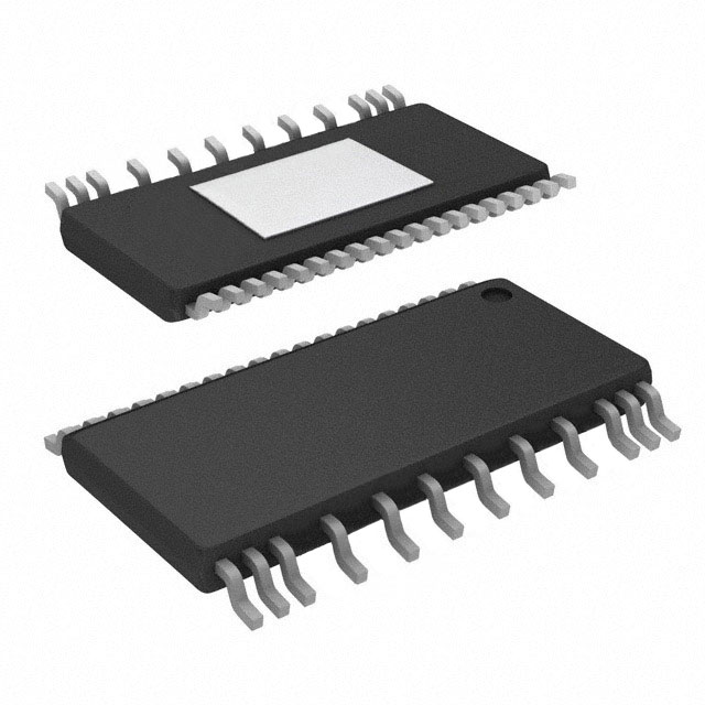
nn Thermally Enhanced FE38 TSSOP Package Modified
for High Voltage Operation
nn
APPLICATIONS
nn
Industrial, Automotive, Medical, Military, Avionics
The LTC®3779 is a high performance buck-boost switching
regulator controller that operates from input voltages
above, below or equal to the output voltage. The constant
frequency current mode architecture allows a phaselockable frequency of up to 600kHz, while an input/
output constant-current loop provides support for battery
charging.
With a wide 4.5V to 150V input and output range and
seamless transfers between operating regions, the
LTC3779 is ideal for automotive, telecom and batterypowered systems.
The LTC3779 features a precision 1.2V reference and
power good output indicator. The MODE pin can select
between pulse-skipping mode or forced continuous mode
of operation. Pulse-skipping mode offers high efficiency
at light load while forced continuous mode operates at
a constant frequency for noise sensitive applications.
The PLLIN pin allows the IC to be synchronized to an
external clock. The SS pin ramps the output voltage
during start-up. Current foldback limits MOSFET heat
dissipation during short-circuit conditions.
All registered trademarks and trademarks are the property of their respective owners.
TYPICAL APPLICATION
VIN
20V TO 120V
4mΩ
VOUT
48V
10A
5µF
30µF
1k
VINSNS
5Ω
Efficiency and Power Loss
vs Input Voltage
56µF
BOOST1
VIN
0.22µF
0.1µF
30
100
15µH
SW1
TG1
10k
133k
98
BG1
RUN
1.21k
100Ω
SENSEP
220pF
NDRV
DRVCC
10µF
LTC3779
475k
SENSEN
SGND
4mΩ
100Ω
PGND
24
EFFICIENCY
96
18
94
12
POWER LOSS (W)
VINOV
EFFICIENCY (%)
20µF
BG2
V5
2.2µF
SS
0.1µF
FREQ
56.2k
100pF
10k
10nF
VOUT = 48V
IOUT = 10A
0.22µF
SW2
90
TG2
100Ω
IAVGSNSP
ITH
6
92
BOOST2
4.7µF
IAVGSNSN
VOUTSNS
0
POWER LOSS
0
12 24 36 48 60 72 84 96 108 120
VIN VOLTAGE (V)
3779 TA01b
100Ω
1k
VFB
3779 TA01a
12.1k
Rev A
Document Feedback
For more information www.analog.com
1
�LTC3779
ABSOLUTE MAXIMUM RATINGS
PIN CONFIGURATION
(Note 1)
Input Supply Voltage (VIN)........................ 150V to –0.3V
Topside Driver Voltage
BOOST1, BOOST2......................................161V to –0.3V
Switch Voltage SW1, SW2........................... 150V to –5V
RUN.......................................................... 150V to –0.3V
IAVGSNSP , IAVGSNSN.....................................150V to –10V
VINSNS, VOUTSNS....................................... 150V to –0.3V
EXTVCC Voltage......................................... 36V to –0.3V
NDRV Voltage..................................................... (Note 9)
DRVCC Voltage.............................................11V to –0.3V
BOOST1-SW1, BOOST2-SW2.......................11V to –0.3V
TG1-SW1, TG2-SW2, BG1, BG2........................... (Note 8)
V5 Voltage.................................................... 6V to –0.3V
MODE, PLLIN, SS, PGOOD........................... V5 to –0.3V
ITH, FREQ, DRVSET...................................... V5 to –0.3V
SENSEP, SENSEN, VINOV............................. V5 to –0.3V
VFB Voltage................................................ 2.7V to –0.3V
Operating Junction Temperature
Range (Notes 2, 3).................................. –40°C to 150°C
Storage Temperature Range................... –65°C to 150°C
EXTVCC /DRVCC Peak Current...............................100mA
ORDER INFORMATION
TOP VIEW
BG1
1
38 SW1
VINOV
2
37 TG1
DRVSET
3
36 BOOST1
SGND
4
EXTVCC
5
NDRV
6
DRVCC
7
V5
8
SS
9
VFB 10
SENSEP 11
34 VIN
32 VINSNS
39
PGND
30 VOUTSNS
28 IAVGSNSN
SENSEN 12
ITH 13
26 IAVGSNSP
SGND 14
MODE 15
24 RUN
PLLIN 16
FREQ 17
22 BOOST2
PGOOD 18
21 TG2
BG2 19
20 SW2
FE PACKAGE
VARIATION: FE38(31)
38-LEAD PLASTIC TSSOP
TJMAX = 150°C, θJA = 28°C/W
EXPOSED PAD (PIN 39) IS PGND, MUST BE SOLDERED TO PCB
FOR RATED ELECTRICAL AND THERMAL CHARACTERISTICS
http://www.linear.com/product/LTC3779#orderinfo
LEAD FREE FINISH
TAPE AND REEL
PART MARKING
PACKAGE DESCRIPTION
TEMPERATURE RANGE
LTC3779EFE#PBF
LTC3779EFE#TRPBF
LTC3779FE
38-Lead Plastic TSSOP
–40°C to 125°C
LTC3779IFE#PBF
LTC3779IFE#TRPBF
LTC3779FE
38-Lead Plastic TSSOP
–40°C to 125°C
LTC3779HFE#PBF
LTC3779HFE#TRPBF
LTC3779FE
38-Lead Plastic TSSOP
–40°C to 150°C
Consult ADI Marketing for parts specified with wider operating temperature ranges.
For more information on lead free part marking, go to: http://www.linear.com/leadfree/
For more information on tape and reel specifications, go to: http://www.linear.com/tapeandreel/. Some packages are available in 500 unit reels through
designated sales channels with #TRMPBF suffix.
Rev A
2
For more information www.analog.com
�LTC3779
ELECTRICAL CHARACTERISTICS
The l denotes the specifications which apply over the specified operating
junction temperature range, otherwise specifications are at TA = 25°C (Note 2), VIN = 15V, VRUN = 5V, VEXTVCC = 0V, VDRVSET = 0V,
VVINOV = 0V unless otherwise noted.
SYMBOL
PARAMETER
CONDITIONS
MIN
MAX
UNITS
VIN
Input Supply Operating Voltage Range
(Note 4)
4.5
150
V
VOUT
Output Supply Operating Voltage Range
1.2
150
V
IQ
1.188
TYP
1.2
1.212
V
–15
-50
nA
Regulated Feedback Voltage
(Note 5); ITH Voltage = 1.4V
Feedback Current
(Note 5)
Reference Voltage Line Regulation
(Note 5); VIN = 7V to 100V
Output Voltage Load Regulation
(Note 5); Measured in Servo Loop; ∆ITH
Voltage = 1.5V to 2V
Transconductance Amplifier gm
(Note 5); ITH = 1.4V; Sink/Source 5µA
1.5
Input DC Supply Current
(Note 6)
3.6
Shutdown
RUN = 0V
Undervoltage Lockout
V5 Ramping Up
4.1
V5 Ramping Down
3.6
VRUN Rising
1.1
RUN Pin ON Threshold
l
l
RUN Pin Hysteresis
0.02
0.2
%
0.01
0.2
%
mmho
5.5
mA
40
75
µA
4.35
4.6
V
3.85
4.1
V
1.2
1.3
100
V
mV
RUN Pin Source Current
VRUN < 1.2V
2.5
µA
RUN Pin Hysteresis Current
VRUN > 1.2V
6.5
µA
VIN Overvoltage Lockout Threshold
(Rising)
VVINOV Rising
1.18
VIN Overvoltage Hysteresis
1.28
1.38
50
V
mV
SENSE Pins Current
VSENSEP = VSENSEN = 0
±2
µA
IAVGSNS Pins Current
VIAVGSNSP = VIAVGSNSN = 10V
15
µA
Soft-Start Charge Current
VSS = 0V
Maximum Current Sense Threshold
(Buck Region Valley Current Mode)
VFB = 1V
Maximum Current Sense Threshold
(Boost Region Peak Current Mode)
VFB = 1V
Maximum Input / Output Average
Current Sense Threshold
VIAVGSNSP = VIAVGSNSN = 10V, VFB = 1V
Maximum Duty Factor
% Switch C On
90
%
DCON(MIN, BOOST) Minimum Duty Factor for Main Switch in % Switch C On
Boost Operation
9
%
Minimum Duty Factor for Main Switch in % Switch B On
Buck Operation
9
%
IAVGSNSP
IAVGSNSN
VSENSE(MAX)
DC(MAX, BOOST)
DCON(MIN, BUCK)
4
5
6
µA
l
70
90
110
mV
l
120
140
160
mV
47.5
50
52.5
mV
Gate Driver
TG Pull-Up On Resistance
TG Pull-Down On Resistance
VDRVCC = 9V
3.1
1.3
Ω
BG Pull-Up On Resistance
BG Pull-Down On Resistance
VDRVCC = 9V
5.5
3
Ω
TG Transition Time:
Rise Time
Fall Time
VDRVCC = 9V (Note 7)
CLOAD = 3300pF
60
ns
BG Transition Time:
Rise Time
Fall Time
VDRVCC = 9V (Note 7)
CLOAD = 3300pF
60
ns
Rev A
For more information www.analog.com
3
�LTC3779
ELECTRICAL CHARACTERISTICS
The l denotes the specifications which apply over the specified operating
junction temperature range, otherwise specifications are at TA = 25°C (Note 2), VIN = 15V, VRUN = 5V, VEXTVCC = 0V, VDRVSET = 0V,
VVINOV = 0V unless otherwise noted.
SYMBOL
PARAMETER
CONDITIONS
MIN
TYP
MAX
UNITS
Top Gate Off to Bottom Gate On Delay
Synchronous Switch-On Delay Time
CLOAD = 3300pF Each Driver, VDRVSET = V5
60
ns
Bottom Gate Off to Top Gate On Delay
Top Switch-On Delay Time
CLOAD = 3300pF Each Driver, VDRVSET = V5
60
ns
DRVCC LDO Regulator
VDRVCC
VEXTVCC
DRVCC Regulation Voltage from NDRV
Regulator
NDRV Driving External NFET, VEXTVCC = 0V
7V < VIN < 150V, VDRVSET = 0V
8V < VIN < 150V, VDRVSET = 1/4 VV5
9V < VIN < 150V, VDRVSET = Float
10V < VIN < 150V, VDRVSET = 3/4 VV5
11V < VIN < 150V, VDRVSET = VV5
5.8
6.8
7.8
8.75
9.65
6.1
7.1
8.1
9.1
10
6.4
7.4
8.4
9.45
10.35
V
V
V
V
V
DRVCC Regulation Voltage from Internal
VIN LDO
VNDRV = VDRVCC, VEXTVCC = 0V
7V < VIN < 150V, VDRVSET = 0V
8V < VIN < 150V, VDRVSET = 1/4 VV5
9V < VIN < 150V, VDRVSET = Float
10V < VIN < 150V, VDRVSET = 3/4 VV5
11V < VIN < 150V, VDRVSET = VV5
5.5
6.5
7.5
8.45
9.15
5.8
6.8
7.8
8.8
9.5
6.1
7.1
8.1
9.15
9.85
V
V
V
V
V
DRVCC Load Regulation from VIN LDO
DRVCC Regulation Voltage from Internal
EXTVCC LDO
ICC = 0mA to 50mA, VEXTVCC = 0V
0.5
2
%
6.1
7.1
8.1
9.1
10
6.4
7.4
8.4
9.45
10.35
V
V
V
V
V
DRVCC Load Regulation from Internal
EXTVCC LDO
ICC = 0mA to 50mA, VEXTVCC = 12V
VDRVSET = 0V
0.5
2
%
EXTVCC LDO Switchover Voltage
EXTVCC Ramping Positive
EXTVCC Hysteresis
% of DRVCC Regulation Voltage
7V < VEXTVCC < 30V, VDRVSET = 0V
8V < VEXTVCC < 30V, VDRVSET = 1/4 VV5
9V < VEXTVCC < 30V, VDRVSET = Float
10V < VEXTVCC < 30V, VDRVSET = 3/4 VV5
11V < VEXTVCC < 30V, VDRVSET = VV5
5.8
6.8
7.8
8.75
9.65
DRVCC – 0.5
V
10
%
V5 Linear Regulator
V5 Regulation Voltage
6V < VDRVCC < 10V
V5 Load Regulation
IV5 = 0mA to 20mA, VDRVCC = 10V
5.3
5.5
5.7
V
0.5
1
%
250
275
kHz
Oscillator and Phase-Locked Loop
Nominal Frequency
RFREQ = 68.5kΩ
225
Low Fixed Frequency
RFREQ ≤ 20kΩ
30
40
50
kHz
High Fixed Frequency
RFREQ = 135kΩ
450
500
550
kHz
PLLIN Input Threshold
VPLLIN Rising
VPLLIN Falling
1.2
V
V
2
PLLIN Input Resistance
Synchronizable Oscillator Frequency
IFREQ
200
PLLIN = External Clock
Frequency Setting Current
l
50
l
18
kΩ
600
kHz
20
22
µA
0.1
0.3
V
±1
µA
PGOOD Output
PGOOD Voltage Low
IPGOOD = 2mA
PGOOD Leakage Current
VPGOOD = 5.5V
PGOOD Trip Level
VFB with Respect to Set Regulated Voltage
PGOOD delay
VFB Ramping Negative
–10
%
VFB Ramping Positive
10
%
VPGOOD High to Low
125
µs
Rev A
4
For more information www.analog.com
�LTC3779
ELECTRICAL CHARACTERISTICS
Note 1: Stresses beyond those listed under Absolute Maximum Ratings
may cause permanent damage to the device. Exposure to any Absolute
Maximum Rating condition for extended periods may affect device
reliability and lifetime.
Note 2: The LTC3779 is tested under pulsed load conditions such that TJ
≈ TA. The LTC3779E is guaranteed to meet performance specifications
from 0°C to 85°C junction temperature. Specifications over the –40°C
to 125°C operating junction temperature range are assured by design,
characterization and correlation with statistical process controls. The
LTC3779I is guaranteed over the full –40°C to 125°C operating junction
temperature range. The LTC3779H is guaranteed over the full –40°C to
150°C operating junction temperature range. High junction temperature
degrades operating lifetimes; operating lifetime is derated for junction
temperatures greater than 125°C. Note that the maximum ambient
temperature consistent with these specifications is determined by
specific operating conditions in conjunction with board layout, the rated
package thermal impedance and other environmental factors. The junction
temperature TJ is calculated from the ambient temperature TA and power
dissipation PD according to the formula:
TJ = TA + (PD • θJA),
where θJA = 28°C/W for the TSSOP package.
Note 3: This IC includes over temperature protection that is intended to
protect the device during momentary overload conditions. The maximum
rated junction temperature will be exceeded when this protection is active.
Continuous operation above the specified absolute maximum operating
junction temperature may impair device reliability or permanently damage
the device.
Note 4: When biased from an auxiliary supply through the EXTVCC pin, the
LTC3779 can operate from a VIN voltage lower than 4.5V. Otherwise the
minimum VIN operational voltage is 4.5V after startup.
Note 5: The LTC3779 is tested in a feedback loop that servos VITH to a
specified voltage and measures the resultant VFB.
Note 6: Dynamic supply current is higher due to the gate charge being
delivered at the switching frequency. See Applications Information.
Note 7: Rise and fall times are measured using 10% and 90% levels.
Delay times are measured using 50% levels.
Note 8: Do not apply a voltage or current source to these pins. They must
be connected to capacitive loads only, otherwise permanent damage may
occur. These pins are rated for an absolute maximum voltage of –0.3V to
11V.
Note 9: Do not apply a voltage or current source to the NDRV pin, other
than tying NDRV to DRVCC when not used. If used it must be connected
to capacitive loads only (see DRVCC Regulator in the Applications
Information section), otherwise permanent damage may occur.
Rev A
For more information www.analog.com
5
�LTC3779
TYPICAL PERFORMANCE CHARACTERISTICS
Efficiency and Power Loss
vs Load Current and Input Voltage
Continuous Mode
96
EFFICIENCY (%)
VIN = 72V
VIN = 48V
VIN = 24V
5
4
72
3
68
2
64
8
6
94
EFFICIENCY
4
91
POWER LOSS
2
88
1
POWER LOSS
60
0.1
1
LOAD CURRENT (A)
FIGURE 18 CIRCUIT
10
0
85
5
10 15 20 25 30 35 40 45 50 55
VIN VOLTAGE (V)
Load Step Boost Region
Pulse-Skipping Mode
Load Step Buck-Boost Region
Continuous Mode
ILOAD
5A/DIV
ILOAD
5A/DIV
ILOAD
5A/DIV
IL
5A/DIV
IL
5A/DIV
IL
5A/DIV
VOUT
1V/DIV
AC-COUPLED
VOUT
1V/DIV
AC-COUPLED
VOUT
1V/DIV
AC-COUPLED
200µs/DIV
3779 G03
VIN = 36V
VOUT = 48V
Load Step Buck-Boost Region
Pulse-Skipping Mode
200µs/DIV
3779 G04
VIN = 48V
VOUT = 48V
Load Step Buck Region
Continuous Mode
ILOAD
5A/DIV
ILOAD
5A/DIV
IL
5A/DIV
IL
5A/DIV
IL
5A/DIV
VOUT
1V/DIV
AC-COUPLED
VOUT
1V/DIV
AC-COUPLED
VOUT
1V/DIV
AC-COUPLED
200µs/DIV
3779 G06
VIN = 120V
VOUT = 48V
200µs/DIV
200µs/DIV
3779 G05
Load Step Buck Region
Pulse-Skipping Mode
ILOAD
5A/DIV
VIN = 48V
VOUT = 48V
0
3779 G02
3779 G01
Load Step Boost Region
Continuous Mode
VIN = 36V
VOUT = 48V
10
POWER LOSS (W)
6
84
POWER LOSS (W)
7
FIGURE 17 CIRCUIT
97
8
88
76
VOUT = 12V
IOUT = 5A
9
VOUT = 48V
fSW = 250kHz
92
80
100
10
EFFICIENCY
EFFICIENCY (%)
100
Efficiency and Power Loss
vs Input Voltage
3779 G07
VIN = 120V
VOUT = 48V
200µs/DIV
3779 G08
Rev A
6
For more information www.analog.com
�LTC3779
TYPICAL PERFORMANCE CHARACTERISTICS
Forced Continuous Mode
Boost Region
Forced Continuous Mode
Buck-Boost Region
Pulse-Skipping Mode
Boost Region
SW1
100V/DIV
SW1
100V/DIV
SW1
100V/DIV
SW2
100V/DIV
SW2
100V/DIV
SW2
100V/DIV
IL
5A/DIV
IL
5A/DIV
IL
1A/DIV
VOUT
200mV/DIV
AC-COUPLED
VOUT
200mV/DIV
AC-COUPLED
VOUT
200mV/DIV
AC-COUPLED
VIN = 24V
VOUT = 48V
ILOAD = 0A
5µs/DIV
3779 G09
VIN = 24V
VOUT = 48V
ILOAD = 0A
5µs/DIV
3779 G10
VIN = 48V
VOUT = 48V
ILOAD = 0A
Forced Continuous Mode
Buck Region
Pulse-Skipping Mode
Buck-Boost Region
SW1
100V/DIV
SW1
100V/DIV
SW2
100V/DIV
SW2
100V/DIV
SW2
100V/DIV
IL
1A/DIV
IL
5A/DIV
IL
5A/DIV
VOUT
200mV/DIV
AC-COUPLED
VOUT
200mV/DIV
AC-COUPLED
VOUT
200mV/DIV
AC-COUPLED
5µs/DIV
3779 G12
VIN = 120V
VOUT = 48V
ILOAD = 0A
Start-Up from RUN
Forced Continuous Mode
Pre-Biased Output
5µs/DIV
3779 G13
VIN = 120V
VOUT = 48V
ILOAD = 0A
Start-Up Forced Continuous Mode
Boost Region
SW1
50V/DIV
SW1
100V/DIV
SW2
50V/DIV
SW2
100V/DIV
IL
5A/DIV
IL
500mA/DIV
IL
500mA/DIV
VOUT
50V/DIV
VOUT
50V/DIV
VOUT
50V/DIV
3779 G15
5ms/DIV
VIN = 24V
VOUT = 48V
15Ω RESISTIVE LOAD
3779 G16
5µs/DIV
3779 G14
Start-Up Forced Continuous Mode
Buck-Boost Region
SW1
100V/DIV
SW2
100V/DIV
2.5ms/DIV
VIN = 24V
VOUT = 48V
VOUT PRE-BIAS = 12V
200mA LOAD
3779 G11
Pulse-Skipping Mode
Buck Region
SW1
100V/DIV
VIN = 48V
VOUT = 48V
ILOAD = 0A
5µs/DIV
5ms/DIV
VIN = 48V
VOUT = 48V
15Ω RESISTIVE LOAD
3779 G17
Rev A
For more information www.analog.com
7
�LTC3779
TYPICAL PERFORMANCE CHARACTERISTICS
Shutdown from RUN
Forced Continuous Mode
Boost Region
Start-Up Forced Continuous Mode
Buck Region
SW1
100V/DIV
SW2
100V/DIV
IL
500mA/DIV
VOUT
50V/DIV
5ms/DIV
VIN = 120V
VOUT = 48V
15Ω RESISTIVE LOAD
Shutdown from RUN
Pulse-Skipping Mode
Boost Region
RUN
5V/DIV
RUN
5V/DIV
SW1
100V/DIV
SW2
100V/DIV
IL
20A/DIV
SW1
100V/DIV
SW2
100V/DIV
IL
20A/DIV
VOUT
50V/DIV
VOUT
50V/DIV
3779 G18
200µs/DIV
VIN = 24V
VOUT = 48V
5A LOAD
Shutdown from RUN
Forced Continuous Mode
Buck-Boost Region
3779 G19
Shutdown from RUN
Forced Continuous Mode
Buck Region
RUN
5V/DIV
SW1
100V/DIV
SW1
100V/DIV
VIN
100V/DIV
12V to 120V
SW2
100V/DIV
IL
2A/DIV
SW2
100V/DIV
IL
20A/DIV
ITH
2V/DIV
IL
1A/DIV
VOUT
50V/DIV
VOUT
50V/DIV
VOUT
500mV/DIV
AC-COUPLED
200µs/DIV
3779 G21
Line Transient Falling Edge
10.5
IL
1A/DIV
VOUT
500mV/DIV
AC-COUPLED
1ms/DIV
1ms/DIV
VOUT = 48V
6.5
VIN LDO (No NDRV FET), EXTVCC = 0V
NDRV LDO (NDRV FET), EXTVCC = 0V
EXTVCC = 12V (No NDRV FET)
DRVCC VOLTAGE (V)
DRVCC VOLTAGE (V)
ITH
2V/DIV
3779 G22
DRVCC vs Load Current
VIN
100V/DIV
VOUT = 48V
200µs/DIV
VIN = 120V
VOUT = 48V
ILOAD = 5A
3779 G20
Line Transient Rising Edge
RUN
5V/DIV
VIN = 48V
VOUT = 48V
NO LOAD
200µs/DIV
VIN = 24V
VOUT = 48V
5A LOAD
10.0
9.5
3779 G23
DRVCC vs Load Current
label2
label5
label4
label3
VIN LDO (No NDRV FET), EXTVCC = 0V
NDRV LDO (NDRV FET), EXTVCC = 0V
EXTVCC = 8.5V (No NDRV FET)
6.0
5.5
3779 G24
9.0
VIN = 12V
DRVSET = V5
0
20
40
60
80
LOAD CURRENT (mA)
100
3779 G25
5.0
VIN = 12V
DRVSET = 0V
0
20
40
60
80
LOAD CURRENT (mA)
100
3779 G26
Rev A
8
For more information www.analog.com
�LTC3779
TYPICAL PERFORMANCE CHARACTERISTICS
VINOV Transient Forced
Continuous Mode Buck Region
Peak Current Threshold vs VITH
(Boost)
Current Foldback Limit
IL
10A/DIV
VOUT
50V/DIV
3779 G27
10ms/DIV
VIN = 120V
VOUT = 48V
50Ω RESISTIVE LOAD
200
BOOST
150
100
50
0
–50
–100
BUCK
–150
0
CURRENT LIMIT (SENSEP – SENSEN) (mV)
SW2
100A/DIV
CURRENT LIMIT (SENSEP – SENSEN) (mV)
200
SW1
100V/DIV
150
100
50
0
–50
–100
–150
0.1 0.2 0.3 0.4 0.5 0.6 0.7 0.8 0.9 1.0
VFB (V)
0
0.4
0.8
3779 G28
Valley Current Threshold vs VITH
(Buck)
0
–50
–100
0
100
BOOST
50
0
–50
BUCK
1210
1200
1190
0
25 50 75 100 125 150
TEMPERATURE (°C)
1180
–50 –25
V5 Low Dropout Regulation
Voltage vs Temperature
12
4.1
4.0
3.9
3.8
5.6
10
DRVCC (V)
RISING
5.5
EXTVCC = 30V
9
8
DRVSET = V5
DRVSET = 3/4 • V5
DRVSET = 1/2 • V5
DRVSET = 1/4 • V5
7
5.4
DRVSET = GND
FALLING
0
EXTVCC LDO vs Temperature
11
V5 LDO VOLTAGE (V)
UVLO THRESHOLD (V)
4.3
3.6
–50 –25
25 50 75 100 125 150
TEMPERATURE (°C)
3779 G32
5.7
3.7
0
3779 G31
Undervoltage Lockout Threshold
(V5) vs Temperature
4.2
3779 G29
–100
3779 G30
4.4
2.8
150
–150
–50 –25
0.2 0.4 0.6 0.8 1.1 1.3 1.5 1.7 1.9 2.1
VITH (V)
2.4
1220
FEEDBACK VOLTAGE (mV)
CURRENT LIMIT (SENSEP – SENSEN) (mV)
CURRENT LIMIT (SENSEP – SENSEN) (mV)
200
50
2.0
Regulated Feedback Voltage
vs Temperature
Maximum Current Limit
vs Temperature
100
1.2 1.6
VITH (V)
6
25 50 75 100 125 150
TEMPERATURE (°C)
5.3
–50 –25
0
25 50 75 100 125 150
TEMPERATURE (°C)
3779 G33
3779 G34
5
–50 –25
0
25 50 75 100 125 150
TEMPERATURE (°C)
3779 G35
Rev A
For more information www.analog.com
9
�LTC3779
TYPICAL PERFORMANCE CHARACTERISTICS
NDRV LDO vs Temperature
12
800
11
11
700
DRVSET = V5, VIN = 11V
10
DRVCC (V)
DRVSET = 3/4 • V5, VIN = 10V
9
DRVSET = 1/2 • V5, VIN = 9V
8
DRVSET = 1/4 • V5, VIN = 8V
7
DRVSET = GND, VIN = 7V
6
5
–50 –25
0
25 50 75 100 125 150
TEMPERATURE (°C)
DRVSET = V5, VIN = 11V
9
DRVSET = 3/4 • V5, VIN = 10V
8
DRVSET = 1/2 • V5, VIN = 9V
7
DRVSET = 1/4 • V5, VIN = 8V
6
DRVSET = GND, VIN = 7V
5
–50 –25
3779 G36
EXTVCC = 0V
SWITCHING FREQUENCY (kHz)
12
10
DRVCC (V)
Oscillator Frequency
vs Temperature
VIN LDO vs Temperature
0
600
RFREQ = 120k
500
400
300
RFREQ = 67.5k
200
100
25 50 75 100 125 150
TEMPERATURE (°C)
FREQ = V5
RFREQ = 27.5k
0
–50 –25
0
25 50 75 100 125 150
TEMPERATURE (°C)
3779 G38
3779 G37
Frequency Setting Current
vs Temperature
FREQ = GND
Input Supply Current
vs Temperature
5
20.5
20.4
4
SUPPLY CURRENT (mA)
20.3
IFREQ (µA)
20.2
20.1
20.0
19.9
19.8
3
2
1
19.7
19.6
19.5
–50 –25
0
0
–50 –25
25 50 75 100 125 150
TEMPERATURE (°C)
VFREQ = 0.8V
3779 G40
Soft-Start Pull-Up Current
vs Temperature
5.2
1.4
SS PULL–UP CURRENT (µA)
RUN THRESHOLD (V)
ON
OFF
1.2
1.1
1.0
0.9
–50 –25
25 50 75 100 125 150
TEMPERATURE (°C)
3779 G39
RUN Threshold vs Temperature
1.3
0
0
25 50 75 100 125 150
TEMPERATURE (°C)
5.1
5.0
4.9
–50 –25
3779 G41
0
25 50 75 100 125 150
TEMPERATURE (°C)
3779 G42
Rev A
10
For more information www.analog.com
�LTC3779
PIN FUNCTIONS
BG1/BG2 (Pins 1 and 19): Bottom Gate Driver Outputs.
This pin drives the gate(s) of the bottom N-Channel
MOSFET between PGND to DRVCC.
VINOV (Pin 2): Connect to the input supply through a
resistor divider to set the over-voltage lockout level. A
voltage on this pin above 1.28V disables all switching,
and the top GATE pins are held low, the bottom GATE pins
are held high, and VOUT is disconnected from VIN. DRVCC
and V5 regulation is maintained during an over-voltage
event. Normal operation resumes when the voltage on this
pin decreases below 1.23V. Exceeding the VINOV lockout
threshold triggers a soft-start reset, resulting in a graceful
recovery from an input supply transient. Tie this pin to
ground if the overvoltage function is not used.
DRVSET (Pin 3): Sets the regulated output voltage of the
DRVCC linear regulator from 6V to 10V in 1V increments.
Tying this pin to SGND sets DRVCC to 6V, tying it to
1/4 • V5 sets DRVCC to 7V, while floating this pin sets
DRVCC to 8V, tying it to 3/4 •V5 sets DRVCC to 9V, and
tying it to V5 sets DRVCC to 10V.
SGND (Pins 4 and 14): Signal ground. All feedback
and soft-start connections should return to SGND. For
optimum load regulation, the SGND pin should be Kelvin
connected to the PCB location between the negative
terminals of the output capacitors.
EXTVCC (Pin 5): External Power Input to an Internal LDO
Connected to DRVCC. When the voltage on this pin is
greater than the DRVCC LDO setting minus 500mV, this
LDO bypasses the internal LDO powered from VIN or the
external LDO connected to NDRV. Tie this pin to ground
if the EXTVCC is not used.
NDRV (Pin 6): Drive Output for External Pass Device of
the LDO Regulator connected to DRVCC. Connect to the
gate of an external NMOS pass device. To disable the
external linear regulator, tie NDRV to DRVCC. An internal
charge pump can drive NDRV above VIN for low dropout
performance.
DRVCC (Pin 7): Output of the Internal or External Low
Dropout Regulator. The gate drivers are powered from
this voltage source. The DRVCC voltage is set by the
DRVSET pin. A low ESR 4.7µF (X5R or better) ceramic
bypass capacitor should be connected between DRVCC
and PGND, as close as possible to the IC. Do not use the
DRVCC pin for any other purpose.
V5 (Pin 8): Output of the Internal 5.5V Low Dropout
Regulator. The control circuits are powered from this
voltage. Bypass this pin to SGND with a minimum of
4.7µF low ESR tantalum or ceramic capacitor, as close
as possible to the IC.
SS (Pin 9): Soft-Start Input. The voltage ramp rate at this
pin sets the voltage ramp rate of the regulated voltage.
This pin has a 5μA pull-up current. A capacitor to ground
at this pin sets the ramp time to final regulated output
voltage.
VFB (Pin 10): Error Amplifier Input. The FB pin should be
connected through a resistive divider network to VOUT to
set the output voltage.
SENSEP (Pin 11): The positive input to the differential
current comparator. This pin is normally connected to a
sense resistor at the source of the power MOSFET. The ITH
pin voltage and controlled offsets between the SENSEP
and SENSEN pins, in conjunction with RSENSE , set the
current trip threshold.
SENSEN (Pin 12): The negative input to the differential
current sense comparator. This pin is normally connected
to the ground side of the sense resistor.
ITH (Pin 13): Error Amplifier Output. The current
comparator trip threshold increases with the ITH control
voltage. The ITH pin is also used for compensating the
control loop of the converter.
MODE (Pin 15): Mode Selection pin. Tying this pin to
SGND or below 0.8V enables forced continuous mode.
Tying it to V5 enables pulse-skipping mode.
Rev A
For more information www.analog.com
11
�LTC3779
PIN FUNCTIONS
PLLIN (Pin 16): External Synchronization Input to Phase
Detector. For external sync, apply a clock signal to this pin
and the internal PLL will synchronize the internal oscillator
to the clock. The PLL compensation network is integrated
into the IC. When synchronized to an external clock, the
regulator can operate either in forced continuous or pulseskipping mode. The mode of operation is controlled by
the setting on the MODE pin.
RUN (Pin 24): Enable Control Input. A voltage above 1.2V
turns on the IC. There is a 2.5µA pull-up current on this
pin. Once the RUN pin rises above the 1.2V threshold the
pull-up current increases to 6.5µA. Forcing this pin below
1.1V shuts down the controller. This pin can be tied to VIN
for always-on operation. Do not float this pin.
FREQ (Pin 17): The frequency control pin for the internal
VCO. Frequencies between 50kHz and 600kHz can be
programmed by using a resistor between FREQ and
SGND. The resistor and an internal 20µA source current
create a voltage used by the internal oscillator to set the
frequency.
IAVGSNSN (Pin 28): The negative input to the Input / Output
Average Current Sense Amplifier. Short IAVGSNSP and
IAVGSNSN pins together, and tie them to V5, if this average
current loop function is not used.
PGOOD (Pin 18): Fault indicator Output. Open-drain
output that pulls to ground when the voltage on the VFB
pin is not within ±10% of its set point.
SW1, SW2 (Pins 38 and 20): Switch Node Connections
to the Inductors.
TG1, TG2 (Pin 37 and 21): High Current Gate Drives
for Top N-Channel MOSFETs. These are the outputs of
floating high side drivers with a voltage swing equal to
DRVCC superimposed on the switch node voltage SW.
BOOST1, BOOST2 (Pin 36 and 22): Boosted Floating
Driver Supplies. The (+) terminal of the bootstrap
capacitor connects to this pin. This pin swings from a
diode drop below DRVCC up to VIN + DRVCC.
IAVGSNSP (Pin 26): The positive input to the Input / Output
Average Current Sense Amplifier.
VOUTSNS (Pin 30): VOUT Sense Input to the Buck-Boost
Transition comparator. Connect this pin to the drain of
the top N-channel MOSFET on the output side through
a 1kΩ resistor.
VINSNS (Pin 32): VIN Sense Input to the Buck-Boost
Transition comparator. Connect this pin to the drain of
the top N-channel MOSFET on the input side.
VIN (Pin 34): Main Supply Pin. A bypass capacitor should
be tied between this pin and the PGND pin.
PGND (Exposed Pad Pin 39): Driver Power Ground.
Connects to the (–) terminal of CIN, COUT and RSENSE.
The exposed pad must be soldered to PCB ground for
electrical contact and rated thermal performance.
Rev A
12
For more information www.analog.com
�LTC3779
BLOCK DIAGRAM
VOUT /BOOST2
VIN /BOOST1
VINOV
+
–
1.2V
2.5µA
RUN
–
+
+
VIN
OV
BOOST2
BOOST1
CA
TG1
FCB
CCM/DCM
IDREV
VIN
DA
BUCK
LOGIC
FET A
D1
SW1
DRVCC
–
SW1
SHDN
DRVCC
BOOST1
CHARGE
CONTROL
BG1
FET B
+
PGND
IREV
RSENSE
BG2
–
FCB
VFLD
VINSNS
VOUTSNS
BUCK/BOOST
TRANSITION
DETECTOR
+
BOOST
LOGIC
DRVCC
FET D
MODE
SELECT
200k
CB
BOOST2
BBT
–
DB
OV/SHDN
IAVGSNSP
A1
CCM
IAVGSNSN
–
SLOPE
DCM
FET C
D2
TG2
ICMP
+
MODE
SW2
DRVCC
RSENSE2
+
IOS
VOUT
–
EA
PLLIN
PHASE DET
5µA
VFB
–
+
+
1.2V
SS
200k
20µA
ITH
FREQ
OSCILLATOR
SENSEP
SENSEN
1.32V
CHARGE
PUMP
VIN
DRVCC LDO
CONTROL
VIN
EN
+
–
NDRV
NDRV LDO
+
–
VIN LDO
+
–
EXTVCC LDO
DRVCC
VFB
1.08V
NDRV
DRVSET
+
–
PGOOD
–
+
+
–
4R
CDRVCC
SGND
V5
UVLO
1R
EXTVCC
DRVSET
V5
LDO
UVLO
V5
3779 BD
CV5
Rev A
For more information www.analog.com
13
�LTC3779
OPERATION
MAIN CONTROL LOOP
The LTC3779 is a current mode controller that provides
an output voltage above, equal to or below the input voltage. The ADI proprietary topology and control architecture
employs a current-sensing resistor. The inductor current
is controlled by the voltage on the ITH pin, which is the
output of the error amplifier EA. The VFB pin receives the
voltage feedback signal, which is compared to the internal
reference voltage by the EA. If the input/output current
regulation loop is implemented, the sensed inductor
current is controlled by either the sensed feedback voltage
or the input/output current.
DRVCC /EXTVCC / V5 Power
Power for the top and bottom MOSFET drivers is derived
from the DRVCC pin. The DRVCC supply voltage can be
programmed from 6V to 10V in 1V steps using the
DRVSET pin. Two separate LDOs (low dropout linear
regulators) can provide power from VIN to DRVCC. The
internal VIN LDO uses an internal P-channel pass device
between the VIN and DRVCC pins. To prevent high on-chip
power dissipation in high input voltage applications, the
LTC3779 also includes an NDRV LDO that utilizes the
NDRV pin to supply power to DRVCC by driving the gate of
an external N-channel MOSFET acting as a linear regulator
with its source connected to DRVCC and drain connected
to VIN. The NDRV LDO includes an internal charge pump
that allows NDRV to be driven above VIN for low dropout
performance.
When the EXTVCC pin is tied to a voltage below its
switchover voltage (DRVCC – 500mV), the VIN and NDRV
LDOs are enabled and one of them supplies power from
VIN to DRVCC. The VIN LDO has a slightly lower regulation
point than the NDRV LDO. If the NDRV LDO is being
used with an external N-channel MOSFET, the gate of the
MOSFET tied to the NDRV pin is driven such that DRVCC
regulates above the VIN LDO regulation point, causing all
DRVCC current to flow through the external N-channel
MOSFET, and bypassing the internal VIN LDO pass device.
If the NDRV LDO is not being used, all DRVCC current
flows through the internal P-channel pass device between
the VIN and DRVCC pins.
If EXTVCC is taken above its switchover voltage, the VIN
and NDRV LDOs are turned off and an EXTVCC LDO is
turned on. Once enabled, the EXTVCC LDO supplies power
from EXTVCC to DRVCC. Using the EXTVCC pin allows the
DRVCC power to be derived from a high efficiency external
source such as the LTC3779 switching regulator output.
Most of the internal circuitry is powered from the V5
rail that is generated by an internal linear regulator from
DRVCC. The V5 pin needs to be bypassed with a 1µF to
10µF external capacitor between V5 and SGND. This pin
provides a 5.5V output that can supply up to 20mA of
current. See the Applications Information section for more
details.
Top MOSFET DRIVER and Internal Charge Path
Each of the two top MOSFET drivers is biased from its
floating bootstrap capacitor, which is normally recharged
by DRVCC through an external diode when the top MOSFET
is turned off and when SW goes low. When the LTC3779
operates exclusively in the buck or boost regions, one
of the top MOSFETs is constantly on. An internal charge
path, from VOUT and BOOST2 to B00ST1 or from VIN and
B00ST1 to B00ST2, charges the bootstrap capacitor so
that the top MOSFET can be kept on. However, if a high
leakage external diode is used such that the internal charge
path cannot provide sufficient charge to the external
bootstrap capacitor, an internal UVLO comparator, which
constantly monitors the drop across the capacitor, will
sense the (BOOST – SW) voltage when it is below the
boost capacitor refresh threshold. This will turn off its top
MOSFET for about one-twelfth of the clock period every
four cycles to allow the bootstrap capacitor to recharge.
The boost capacitor refresh threshold varies with the
DRVSET pin setting.
Shutdown and Start-Up
The LTC3779 can be shut down by pulling the RUN pin
low. Pulling RUN below 1.1V shuts down the main control
loop for the controller and most internal circuits, including
the DRVCC and V5 regulators. Releasing RUN allows an
internal 2.5µA current to pull-up the pin and enable the
controller. When RUN is above the accurate threshold of
1.2V, the internal LDO will power up DRVCC. At the same
Rev A
14
For more information www.analog.com
�LTC3779
OPERATION
time, a 6.5µA pull-up current will kick in to provide more
RUN pin hysteresis. The RUN pin may be externally pulled
up or driven directly by logic. The RUN pin can tolerate up
to 150V (absolute maximum), so it can be conveniently
tied to VIN in always-on applications where the controller
is enabled continuously and never shut down. The RUN
pin will have no internal pull-up current when externally
driven to a voltage above 4V.
between regions is continuous. Hysteresis is added to
prevent chattering when transitioning between regions.
VOUT
VIN
TG1
A
SW1
BG1
D
L
TG2
SW2
B
C
BG2
RSENSE
Soft-Start
3779 F01
The start-up of the controller’s output voltage VOUT is
controlled by the voltage on the SS pin. When the voltage
on the SS pin is less than the 1.2V internal reference,
the LTC3779 regulates the VFB voltage to the SS voltage
instead of the 1.2V reference. This allows the SS pin to
be used to program soft-start by connecting an external
capacitor from the SS pin to SGND. An internal 5µA
pull-up current charges this capacitor, creating a voltage
ramp on the SS pin. As the SS voltage rises linearly from
0V to 1.2V (and beyond), the output voltage VOUT rises
smoothly from zero to its final value. When RUN is pulled
low to disable the controller, or during an overvoltage
event on the VIN input supply or during an overtemperature
shutdown event, or when V5 drops below its undervoltage
lockout threshold of 3.85V, the SS pin is pulled low by
an internal MOSFET. When in undervoltage lockout, the
controller is disabled and the external MOSFETs are held
off.
Certain applications can require the start-up of the
converter into a non-zero load voltage, where residual
charge is stored on the VOUT capacitor at the onset of
converter switching. In order to prevent the VOUT from
discharging under these conditions, the part will be forced
into discontinuous mode of operation until the SS voltage
crosses VFB or 1.32V, whichever is lower.
Power Switch Control
Figure 1 shows a simplified diagram of how the four power
switches are connected to the inductor, VIN, VOUT and GND.
Figure 2 shows the regions of operation for the LTC3779
as a function of VOUT – VIN or switch duty cycle, DC. The
power switches are properly controlled so the transfer
Figure 1. Simplified Diagram of the Output Switches
DCMAX
BOOST
DCMIN
BOOST
DCMAX
BUCK
A ON, B OFF
PWM C, D SWITCHES
BOOST REGION
FOUR SWITCH PWM
BUCK/BOOST REGION
D ON, C OFF
PWM A, B SWITCHES
BUCK REGION
DCMIN
BUCK
3779 F02
Figure 2. Operating Region vs Duty Cycle
Buck Region (VIN >> VOUT)
When VIN is significantly higher than VOUT, the part will run
in the buck region. In this region switch C is always off. At
the start of every cycle, synchronous switch B is turned on
first. Inductor current is sensed when synchronous switch
B is turned on. After the sensed inductor valley current
falls below a reference voltage, which is proportional to
VITH, synchronous switch B is turned off and switch A
is turned on for the remainder of the cycle. Switches A
and B will alternate, behaving like a typical synchronous
buck regulator. The duty cycle of Switch A increases
until the maximum duty cycle of the converter reaches
DC(MAX_BUCK), given by:
1⎞
⎛
DC(MAX,BUCK) = ⎜ 1− ⎟ • 100% = 91.67%
⎝ 12 ⎠
Rev A
For more information www.analog.com
15
�LTC3779
OPERATION
Figure 3 shows the typical buck region waveforms. If VIN
approaches VOUT, the buck-boost region is reached.
CLOCK
SWITCH A
SWITCH B
LOW
SWITCH C
HIGH
SWITCH D
IL
3779 F03
Figure 3. Buck Region (VIN >> VOUT)
Buck-Boost Region (VIN ≈ VOUT)
When VIN is close to VOUT, the controller enters the buckboost region. Figure 4 shows the typical waveforms in this
region. At the beginning of a clock cycle, if the controller
starts with B and D on, the controller first operates as if in
the buck region. When ICMP trips, switch B is turned off,
and switch A is turned on. At 120° clock phase, switch C is
turned on. The LTC3779 starts to operate as a boost until
ICMP trips. Then, switch D is turned on for the remainder
of the clock period. If the controller starts with switches
A and C on, the controller first operates as a boost, until
ICMP trips and switch D is turned on. At 120°, switch B is
turned on, making it operate as a buck. Then, ICMP trips,
turning switch B off and switch A on for the remainder of
the clock period.
Boost Region (VIN
(
)
VIN(MIN) • VOUT − VIN(MIN) • 100
f •IOUT(MAX) • %Ripple • VOUT
(
)
2
VOUT • VIN(MAX) − VOUT • 100
f •IOUT(MAX) • %Ripple • VIN(MAX)
H,
H
Ferrite designs have very low core loss and are preferred
at high switching frequencies, so design goals can
concentrate on copper loss and preventing saturation.
Ferrite core material saturates “hard,” which means that
inductance collapses abruptly when the peak design
current is exceeded. This results in an abrupt increase
in inductor ripple current and consequent output voltage
ripple. Do not allow the core to saturate!
CIN and COUT Selection
In the boost region, input current is continuous. In the
buck region, input current is discontinuous. In the buck
region, the selection of input capacitor CIN is driven by
the need to filter the input square wave current. Use a low
ESR capacitor sized to handle the maximum RMS current.
For buck operation, the input RMS current is given by:
where:
f is operating frequency, Hz
% Ripple is allowable inductor current ripple
VIN(MIN) is minimum input voltage, V
VIN(MAX) is maximum input voltage, V
VOUT is output voltage, V
IOUT(MAX) is maximum output load current, A
For high efficiency, choose an inductor with low core loss,
such as ferrite. Also, the inductor should have low DC
resistance to reduce the I2R losses, and must be able to
handle the peak inductor current without saturating. To
minimize radiated noise, use a toroid, pot core or shielded
bobbin inductor.
Inductor Core Selection
Once the inductance value is determined, the type of
inductor must be selected. Core loss is independent of
core size for a fixed inductor value, but it is very dependent
on inductance selected. As inductance increases, core
losses go down. Unfortunately, increased inductance
requires more turns of wire and therefore copper losses
will increase.
IRMS ≈ IOUT(MAX) •
VOUT
VIN
•
−1
VIN
VOUT
This formula has a maximum at VIN = 2VOUT, where
IRMS = IOUT(MAX) / 2. This simple worst-case condition
is commonly used for design because even significant
deviations do not offer much relief. Note that ripple
current ratings from capacitor manufacturers are often
based on only 2000 hours of life which makes it advisable
to derate the capacitor.
In the boost region, the discontinuous current shifts
from the input to the output, so COUT must be capable
of reducing the output voltage ripple. The effects of ESR
(equivalent series resistance) and the bulk capacitance
must be considered when choosing the right capacitor
for a given output ripple voltage. The steady ripple due to
charging and discharging the bulk capacitance is given by:
ΔVRIPPLE(BOOST,CAP) =
(
IOUT(MAX) • VOUT − VIN(MIN)
COUT • VOUT • f
)V
where COUT is the output filter capacitor.
The steady ripple due to the voltage drop across the ESR
is given by:
∆V(BOOST,ESR) = IOUT(MAX,BOOST) • ESR
Rev A
For more information www.analog.com
23
�LTC3779
APPLICATIONS INFORMATION
In buck mode, VOUT ripple is given by:
Multiple capacitors placed in parallel may be needed to
meet the ESR and RMS current handling requirements.
Aluminum electrolytic and ceramic capacitors are
available in surface mount packages. Ceramic capacitors
have excellent low ESR characteristics but can have a high
voltage coefficient. Bulk capacitors are now available with
low ESR and high ripple current ratings, such as OSCON
and aluminum electrolytics with hybrid conductive
polymers.
Power MOSFET Selection and Efficiency
Considerations
2
PA,BOOST
⎛V
⎞
= ⎜ OUT •IOUT(MAX) ⎟ • ρτ • RDS(ON)
⎝ VIN
⎠
where ρt is a normalization factor (unity at 25°C)
accounting for the significant variation in on-resistance
with temperature, typically about 0.4%/°C, as shown in
Figure 11. For a maximum junction temperature of 125°C,
using a value ρt = 1.5 is reasonable.
2.0
The LTC3779 requires four external N-channel power
MOSFETs, two for the top switches (switches A and
D, shown in Figure 1) and two for the bottom switches
(switches B and C, shown in Figure 1). Important
parameters for the power MOSFETs are the breakdown
voltage VBR,DSS, threshold voltage VGS,TH, on-resistance
RDS(ON), reverse transfer capacitance CRSS and maximum
current IDS(MAX).
The peak-to-peak drive levels are set by the DRVCC
voltage. This voltage can range from 6V to 10V depending
on the DRVSET pin setting. Therefore, both logic-level
and standard-level threshold MOSFETs can be used in
most applications, depending on the programmed DRVCC
voltage. Pay close attention to the BVDSS specification for
the MOSFETs as well.
ρT NORMALIZED ON-RESISTANCE (Ω)
⎛
⎞
1
ΔVOUT ≤ ΔIL ⎜ ESR +
8 • f • COUT ⎟⎠
⎝
In order to select the power MOSFETs, the power
dissipated by the device must be known. For switch A,
the maximum power dissipation happens in the boost
region, when it remains on all the time. Its maximum
power dissipation at maximum output current is given by:
1.5
1.0
0.5
0
–50
50
100
0
JUNCTION TEMPERATURE (°C)
150
3779 F11
Figure 11. Normalized RDS(ON) vs Temperature
The LTC3779’s ability to adjust the gate drive level
between 6V to 10V allows an application circuit to be
precisely optimized for efficiency. When adjusting the gate
drive level, the final arbiter is the total input current for
the regulator. If a change is made and the input current
decreases, then the efficiency has improved. If there is
no change in input current, then there is no change in
efficiency.
Rev A
24
For more information www.analog.com
�LTC3779
APPLICATIONS INFORMATION
Switch B operates in the buck region as the synchronous
rectifier. Its power dissipation at maximum output current
is given by:
PB,BUCK =
VIN − VOUT
•IOUT(MAX)2 • ρτ • RDS(ON)
VIN
Switch C operates in the boost region as the control
switch. Its power dissipation at maximum current is given
by:
PC,BOOST =
( VOUT − VIN ) VOUT •I
2
OUT(MAX)
VIN2
•RDS(ON) + k • VOUT3 •
IOUT(MAX)
VIN
• ρτ
• CRSS • f
Schottky Diode (D1, D2) Selection
The Schottky diodes, D1 and D2, shown in the Block
Diagram, conduct during the dead time between the
conduction of the power MOSFET switches. They are
intended to prevent the body diode of synchronous
switches B and D from turning on and storing charge
during the dead time. In particular, D2 significantly
reduces reverse recovery current between switch D
turn-off and switch C turn-on, which improves converter
efficiency and reduces switch C voltage stress. In order
for the diode to be effective, the inductance between it
and the synchronous switch must be as small as possible,
mandating that these components be placed adjacently.
Setting Output Voltage
where CRSS is usually specified by the MOSFET
manufacturers. The constant k, which accounts for the
loss caused by reverse recovery current, is inversely
proportional to the gate drive current and has an empirical
value of 1.7.
The LTC3779 output voltage is set by two external
feedback resistive dividers carefully placed across the
output, as shown in Figure 12. The regulated output
voltage is determined by:
For switch D, the maximum power dissipation happens
in the boost region, when its duty cycle is higher than
50%. Its maximum power dissipation at maximum output
current is given by:
To improve the frequency response, a feed forward
capacitor, CFF, may be used. Great care should be taken
to route the VFB line away from noise sources, such as
the inductor or the SW line.
PD,BOOST
V
= IN
VOUT
VOUT = 1.2V • (1 + RB /RA)
2
⎛V
⎞
• ⎜ OUT •IOUT(MAX) ⎟ • ρτ • RDS(ON)
⎝ VIN
⎠
For the same output voltage and current, switch A has the
highest power dissipation and switch B has the lowest
power dissipation unless a short occurs at the output.
From a known power dissipated in the power MOSFET, its
junction temperature can be obtained using the following
formula:
VOUT
LTC3779
RB
CFF
VFB
RA
3779 F12
Figure 12. Setting Output Voltage
TJ = TA + P • RTH(JA)
The RTH(JA) to be used in the equation normally includes
the RTH(JC) for the device plus the thermal resistance from
the case to the ambient temperature (RTH(JC)). This value
of TJ can then be compared to the original, assumed value
used in the iterative calculation process.
Rev A
For more information www.analog.com
25
�LTC3779
APPLICATIONS INFORMATION
RUN Pin and Overvoltage /Undervoltage Lockout
The LTC3779 is enabled using the RUN pin. It has a rising
threshold of 1.2V with 100mV of hysteresis. Pulling the
RUN pin below 1.1V shuts down the main control loop
for the controller and most internal circuits, including the
DRVCC and V5 LDOs. In this state the LTC3779 draws only
40μA of quiescent current. Releasing the RUN pin allows
an internal 2.5µA current to pull-up the pin and enable the
controller. The RUN comparator itself has about 100mV
of hysteresis. When the voltage on the RUN pin exceeds
1.2V, the current sourced into the RUN pin is switched
from 2.5µA to 6.5µA current. The user can therefore
program both the rising threshold and the amount of
hysteresis using an external resistive divider.
The RUN pin is high impedance above 3V and must be
externally pulled up/down or driven directly by logic, as
shown in Figure 13. The RUN pin can tolerate up to 150V
(absolute maximum), so it can be conveniently tied to VIN
in always-on applications where the controller is enabled
continuously and never shut down.
The RUN and VINOV pins can alternatively be configured
as undervoltage (UVLO) and overvoltage (OVLO) lockouts
on the VIN supply with a resistor divider from VIN to
ground. A simple resistor divider can be used as shown
in Figure 14 to meet specific VIN voltage requirements.
One can program additional hysteresis for the RUN
comparator by adjusting the values of the resistive divider.
The current that flows through the R3-R4-R5 divider
will directly add to the shutdown and active current of
the LTC3779, and care should be taken to minimize
the impact of this current on the overall efficiency of
the application circuit. Resistor values in the megohm
range may be required to keep the impact on quiescent
shutdown current low. To pick resistor values, the sum
total of R3 + R4 + R5 (RTOTAL) should be chosen first
based on the allowable DC current that can be drawn from
VIN.
The individual values of R3, R4 and R5 can then be
calculated from the following equations:
⎛
⎞
1.2V
R5 = RTOTAL • ⎜
⎝ Rising VIN OVLO Threshold ⎟⎠
VIN
SUPPLY
4.7M
LTC3779
RUN
⎛
⎞
1.2V
− R5
R4 = RTOTAL • ⎜
⎝ Rising VIN UVLO Threshold ⎟⎠
LTC3779
RUN
3779 F13
For applications that do not need a precise external OVLO,
the VINOV pin should be tied directly to ground. The RUN
pin in this type of application can be used as an external
UVLO using the following equations with R5 = 0Ω.
Figure 13. RUN Pin Interface to Logic
VIN
⎛ R3 ⎞
VIN(ON) = 1.2V ⎜ 1+ ⎟ − 2.5µ • R3
⎝ R4 ⎠
R3
RUN
R4
LTC3779
VINOV
R5
R3 = RTOTAL − R4 − R5
3779 F14
⎛ R3 ⎞
VIN(OFF) = 1.1V ⎜ 1+ ⎟ − 6.5µ • R3
⎝ R4 ⎠
Figure 14. Adjustable UV and OV Lockout
Rev A
26
For more information www.analog.com
�LTC3779
APPLICATIONS INFORMATION
Similarly, for applications that do not require a precise
UVLO, the RUN pin can be tied to VIN. In this configuration,
the UVLO threshold is limited to the internal VIN UVLO
thresholds as shown in the Electrical Characteristics table.
The resistor values for the OVLO can be computed using
the previous equations with R3 = 0Ω.
Be aware that the VINOV pin cannot be allowed to exceed
its absolute maximum rating of 6V. To keep the voltage on
the VINOV pin from exceeding 6V, the following relation
should be satisfied:
R5
⎛
⎞
VIN(MAX) • ⎜
< 6V
⎝ R3 + R4 + R5 ⎟⎠
Soft-Start
The start-up of VOUT is controlled by the voltage on the SS
pin. If its RUN pin voltage is below 1.1V the controller is in
the shutdown state; its SS pin is actively pulled to ground
in this shutdown state. If the RUN pin voltage is above
1.2V, the controller powers up. A soft-start current of
5μA then starts to charge the SS soft-start capacitor. Note
that soft-start is achieved not by limiting the maximum
output current of the controller but by controlling the
output ramp voltage according to the ramp rate on the
SS pin. When the voltage on the SS pin is less than the
internal 1.2V reference, the LTC3779 regulates the VFB pin
voltage to the voltage on the SS pin instead of the internal
reference. Current foldback is disabled during this phase.
The soft-start range is defined to be the voltage range
from 0V to 1.2V on the SS pin. The total soft-start time
can be calculated as:
⎛ 1.2V ⎞
tSS = CSS • ⎜
⎝ 5µA ⎟⎠
DRVCC Regulator
The LTC3779 features three separate low dropout linear
regulators (LDO) that can supply power at the DRVCC
pin. The internal VIN LDO uses an internal P-channel pass
device between the VIN and DRVCC pins. The internal
EXTVCC LDO uses an internal P-channel pass device
between the EXTVCC and DRVCC pins. The NDRV LDO
utilizes the NDRV pin to drive the gate of an external
N-channel MOSFET acting as a linear regulator with its
drain connected to VIN.
The NDRV LDO provides an alternative method to
supply power to DRVCC from the input supply without
dissipating the power inside the LTC3779 IC. It has an
internal charge pump that allows NDRV to be driven above
the VIN supply, allowing for low dropout performance.
The VIN LDO has a slightly lower regulation point than the
NDRV LDO, such that all DRVCC current flows through the
external N-channel MOSFET (and not through the internal
P-channel pass device) once DRVCC reaches regulation.
When laying out the PC board, care should be taken to
route NDRV away from any switching nodes, especially
SW, TG, and BOOST. Coupling to the NDRV node could
cause its voltage to collapse and the NDRV LDO to lose
regulation. If this occurs, the internal VIN LDO would
take over and maintain DRVCC voltage at a slightly lower
regulation point. However, internal heating of the IC would
become a concern. High frequency noise on the drain of
the external NFET could also couple into the NDRV node
(through the gate-to-drain capacitance of the NDRV NFET)
and adversely affect NDRV regulation. The following are
methods that could mitigate this potential issue (refer to
Figure 15).
1. Add local decoupling capacitors right next to the drain
of the external NDRV NFET in the PCB layout.
2. Insert a resistor (~100Ω) in series with the gate of the
NDRV NFET.
3. Insert a small capacitor (~1nF) between the gate and
source of the NDRV NFET.
When testing the application circuit, be sure the NDRV
voltage does not collapse over the entire input voltage
and output current operating range of the buck-boost
regulator. If the NDRV LDO is not being used, connect
the NDRV pin to DRVCC (Figure 15b).
The DRVCC supply is regulated between 6V to 10V,
depending on the DRVSET pin setting. The internal VIN
and EXTVCC LDOs can supply a peak current of at least
50mA. The DRVCC pin must be bypassed to ground with
a minimum of 4.7μF ceramic capacitor. Good bypassing is
needed to supply the high transient currents required by
Rev A
For more information www.analog.com
27
�LTC3779
APPLICATIONS INFORMATION
VIN
VIN
LTC3779
NDRV
R1*
C2*
C1*
DRVCC
GND
*R1, C1 AND C2 ARE OPTIONAL
3779 F15a
Figure 15a. Configuring the NDRV LDO
Figure 15.
VIN
VIN
NDRV
LTC3779
LDO, NDRV LDO or the EXTVCC LDO. When the voltage on
the EXTVCC pin is less than its switchover threshold (as
determined by the DRVSET pin), the VIN and NDRV LDOs
are enabled. Power dissipation in this case is highest and
is equal to VIN • IDRVCC. If the NDRV LDO is not being
used, this power is dissipated inside the IC. The gate
charge current is dependent on operating frequency as
discussed in the Efficiency Considerations section.
The junction temperature can be estimated by using the
equations given in Note 2 of the Electrical Characteristics
table. For example, if DRVCC is set to 6V, the DRVCC
current is limited to less than 49mA from a 40V supply
when not using the EXTVCC or NDRV LDO’s at a 70°C
ambient temperature:
TJ = 70°C + (49mA)(40V)(28°C/W) = 125°C
DRVCC
To prevent the maximum junction temperature from being
exceeded, the VIN supply current must be checked while
operating in forced continuous mode (MODE = SGND) at
maximum VIN.
GND
3779 F15b
Figure 15b. Disabling the NDRV LDO
the MOSFET gate drivers. The DRVSET pin programs the
DRVCC supply voltage and selects the appropriate EXTVCC
switchover threshold voltages as shown in the Electrical
Characteristics table. The DRVSET pin has five logic level
states. When DRVSET is either grounded, floated or tied to
V5, the typical value for the DRVCC voltage will be 6V, 8V
and 10V respectively. Use the 10V setting with careful PCB
layout. This is because any overshoot between BOOST
and SW would exceed the absolute maximum voltage of
11V for the floating driver. Set DRVSET to one-fourth of
V5 and three-fourths of V5 for 7V and 9V DRVCC voltages.
Please note that the DRVSET pin has an internal 200k
pull-down to SGND and a 200k pull-up to V5. The EXTVCC
turn on threshold is the selected DRVCC regulation voltage
minus 500mV. The turn off threshold is 500mV below the
turn on threshold.
High input voltage applications in which large MOSFETs
are being driven at high frequencies may cause the
maximum junction temperature rating for the LTC3779
to be exceeded. The DRVCC current, which is dominated
by the gate charge current, may be supplied by the VIN
When the voltage applied to EXTVCC rises above its
switchover threshold, the VIN and NDRV LDOs are turned
off and the EXTVCC LDO is enabled. The EXTVCC LDO
remains on as long as the voltage applied to EXTVCC
remains above the switchover threshold minus the
comparator hysteresis. The EXTVCC LDO attempts to
regulate the DRVCC voltage to the voltage as programmed
by the DRVSET pin, so while EXTVCC is less than this
voltage, the LDO is in dropout and the DRVCC voltage is
approximately equal to EXTVCC. When EXTVCC is greater
than the programmed voltage, up to an absolute maximum
of 36V, DRVCC is regulated to the programmed voltage.
Using the EXTVCC LDO allows the MOSFET driver and
control power to be derived from the LTC3779’s switching
regulator output (5.7V ≤ VOUT ≤ 36V) during normal
operation and from the VIN or NDRV LDO when the output
is out of regulation (e.g., start-up, short-circuit).
Significant efficiency and thermal gains can be realized by
powering DRVCC from the output, since the VIN current
resulting from the driver and control currents will be
scaled by a factor of (Duty Cycle)/(Switcher Efficiency).
Rev A
28
For more information www.analog.com
�LTC3779
APPLICATIONS INFORMATION
For 5.5V to 36V regulator outputs, this means connecting
the EXTVCC pin directly to VOUT. Tying the EXTVCC pin
to a 12V supply reduces the junction temperature in the
previous example from 125°C to:
TJ = 70°C + 49mA • (12V) ( 28°C / W ) = 86°C
While using the EXTVCC LDO there is an VIN under voltage
detection circuit that disables the EXTVCC LDO if the VIN
voltage is less that the DRVCC voltage that is set by the
DRVSET pin.
For applications where the minimum VIN voltage of
LTC3779 needs to be less than 4.5V, the EXTVCC pin can
be used to power the VIN of LTC3779. The VIN under
voltage detection circuit is disabled when DRVSET is set
to three-fourths of V5, for 9V DRVCC voltage. Under this
condition the DRVCC voltage can be higher than the VIN
of LTC3779 and an external blocking diode should be
connected from the VIN pin of LTC3779 to the external
VIN supply, to avoid back feeding the VIN supply.
The following list summarizes the four possible
connections for EXTVCC:
1. EXTVCC grounded. This will cause DRVCC to be
powered from the internal VIN or NDRV LDO resulting
in an efficiency penalty of up to 10% at high input
voltages.
2. EXTVCC connected directly to the regulator output.
This is the normal connection for a 5.5V to 36V
regulator and provides the highest efficiency.
3. EXTVCC connected to an external supply. If an external
supply is available in the 5.5V to 36V range, it may be
used to power EXTVCC providing it is compatible with
the MOSFET gate drive requirements.
4. EXTVCC connected to the regulator output through an
external Zener diode. If the output voltage is greater
than 36V, a Zener diode can be used to drop the
necessary voltage between VOUT and EXTVCC such
that EXTVCC remains below 36V (Figure 16). In this
configuration, a bypass capacitor on EXTVCC of at
least 0.1μF is recommended. An optional resistor
between EXTVCC and GND can be inserted to ensure
adequate bias current through the Zener diode.
VOUT > 36V
LTC3779
EXTVCC
EXTVCC < 36V
0.1µF
GND
3779 F16
Figure 16. Using a Zener Diode Between VOUT and EXTVCC
V5 Regulator
An additional P-channel LDO supplies power at the V5
pin from the DRVCC pin. Whereas DRVCC powers the
gate drivers, V5 powers much of the LTC3779’s internal
circuitry. The V5 LDO regulates the voltage at the V5 pin
to 5.5V when DRVCC is at least 6V. The LDO can supply
a peak current of 20mA and must be bypassed to ground
with a minimum of 4.7μF ceramic capacitor or low
ESR electrolytic capacitor. No matter what type of bulk
capacitor is used, an additional 0.1μF ceramic capacitor
placed directly adjacent to the V5 and SGND pins is highly
recommended. V5 is also used as a pull-up to bias other
pins, such as MODE, DRVSET and SS.
Rev A
For more information www.analog.com
29
�LTC3779
APPLICATIONS INFORMATION
Pre-Biased Output Start-Up
There may be situations that require the power supply to
start up with a pre-bias on the output capacitors. In this
case, it is desirable to start up without discharging that
output pre-bias. The LTC3779 can safely power up into a
pre-biased output without discharging it.
If the voltage on the SS pin is lower than VFB, to prevent
pulling current from the output to the input, the LTC3779
forces the part into discontinuous mode of operation
irrespective of the status of the MODE pin. If VFB is
>1.12V, or when the SS voltage crosses VFB or 1.32V,
whichever event happens first, then the MODE pin setting
determines the mode of operation.
Topside MOSFET Driver Supply
In the Block Diagram, the external bootstrap capacitors
CA and CB, connected to the BOOST1 and BOOST2 pins,
supply the gate drive voltage for the topside MOSFET
switches A and D. When the top switch A turns on, the
switch node SW1 rises to VIN and the BOOST1 pin rises
to approximately VIN + DRVCC. When the bottom switch
B turns on, the switch node SW1 is low and the boost
capacitor CA is charged through DA from DRVCC. When
the top switch D turns on, the switch node SW2 rises to
VOUT and the BOOST2 pin rises to approximately VOUT +
DRVCC. When the bottom switch C turns on, switch node
SW2 is low and the boost capacitor CB is charged through
DB from DRVCC. The boost capacitors CA and CB need to
store about 100 times the gate charge required by the top
switches A and D. In most applications, a 0.1µF to 0.47µF,
X5R or X7R dielectric capacitor is adequate.
Fault Conditions: Current Limit and Current Foldback
The maximum inductor current is inherently limited in a
current mode controller by the maximum sense voltage. In
the boost region, maximum sense voltage and the sense
resistance determine the maximum allowed inductor peak
current, which is:
IL(MAX,BOOST) =
140mV
R SENSE
In the buck region, maximum sense voltage and the sense
resistance determine the maximum allowed inductor
valley current, which is:
IL(MAX,BUCK) =
90mV
R SENSE
To further limit current in the event of a short circuit to
ground, the LTC3779 includes foldback current limiting.
If the output falls by more than 50%, then the maximum
sense voltage is progressively lowered to about one-third
of its full value.
Efficiency Considerations
The percent efficiency of a switching regulator is equal to
the output power divided by the input power times 100%.
It is often useful to analyze individual losses to determine
what is limiting the efficiency and which change would
produce the most improvement. Percent efficiency can
be expressed as:
% Efficiency = 100% – (L1 + L2 + L3 + ...)
where L1, L2, etc. a e the individual losses as a percentage
of input power.
Although all dissipative elements in the circuit produce
losses, four main sources usually account for most of the
losses in LTC3779 circuits: 1) IC VIN current, 2) MOSFET
driver current, 3) I2R losses, 4) topside MOSFET transition
losses.
1. The VIN current is the DC supply current given in the
Electrical Characteristics table. VIN current typically
results in a small (1μF) supply bypass capacitors. The
discharged bypass capacitors are effectively put in parallel
with COUT, causing a rapid drop in VOUT. No regulator can
alter its delivery of current quickly enough to prevent this
sudden step change in output voltage if the load switch
resistance is low and it is driven quickly. If the ratio of
CLOAD to COUT is greater than 1:50, the switch rise time
should be controlled so that the load rise time is limited
to approximately 25 • CLOAD. Thus a 10μF capacitor would
require a 250μs rise time, limiting the charging current
to about 200mA.
PC Board Layout Checklist
When laying out the printed circuit board, the following
checklist should be used to ensure proper operation of
the IC.
1. Are the signal and power grounds kept separate?
The combined IC signal ground pin and the ground
return of CDRVCC must return to the combined COUT
(–) terminals. The path formed by the top N-channel
MOSFET, bottom N-channel MOSFET and the CIN
capacitor should have short leads and PC trace
lengths. The output capacitor (–) terminals should
be connected as close as possible to the (–) terminals
of the input capacitor by placing the capacitors next
to each other.
2. Does the LTC3779 VFB pin’s resistive divider connect
to the (+) terminal of COUT? The resistive divider must
be connected between the (+) terminal of COUT and
signal ground. The feedback resistor connections
should not be along the high current input feeds from
the input capacitor(s).
3. Are the SENSEN and SENSEP leads routed together
with minimum PC trace spacing? The filter capacitor
between SENSE+ and SENSE– should be as close as
possible to the IC. Ensure accurate current sensing
with Kelvin connections at the SENSE resistor.
4. Is the DRVCC and decoupling capacitor connected
close to the IC, between the DRVCC and the ground
pin? This capacitor carries the MOSFET drivers’
current peaks.
5. Keep the SW, TG, and BOOST nodes away from
sensitive small-signal nodes. All of these nodes have
very large and fast moving signals and therefore
should be kept on the output side of the LTC3779
and occupy minimum PC trace area.
6. The path formed by switch A, switch B, D1 and the
CIN capacitor should have short leads and PC trace
lengths. The path formed by switch C, switch D, D2
and the COUT capacitor also should have short leads
and PC trace lengths.
7. Use a modified star ground technique: a low
impedance, large copper area central grounding
point on the same side of the PC board as the input
and output capacitors with tie-ins for the bottom of
the DRVCC decoupling capacitor, the bottom of the
voltage feedback resistive divider and the GND pin of
the IC.
Rev A
32
For more information www.analog.com
�LTC3779
APPLICATIONS INFORMATION
Design Example
The RSENSE resistor value can be calculated by using the
maximum current sense voltage specification with some
accommodation for tolerances.
VIN = 6V to 100V
VOUT = 12V
IOUT(MAX) = 5A
f = 200kHz
Maximum ambient temperature = 60°C
RSENSE =
VOUT
f •L
IRIPPLE,BUCK =
IOUT
%
VIN ⎛
V ⎞
• ⎜ 1– IN ⎟
f •L ⎝
VOUT ⎠
IRIPPLE,BOOST =
∆I L,BOOST • 100
I IN
Output voltage is 12V. Select RA as 12.1k. RB is:
V
• RA
RB = OUT
– RA
1.2
Selecting MOSFET Switches
The highest value of ripple current occurs at the maximum
input voltage. In the boost region, the ripple current is:
∆IL,BOOST =
Adding an additional 30% margin, choose RSENSE to be
13.3mΩ/1.3 = 10mΩ.
Select RB as 110k. Both RA and RB should have a tolerance
of no more than 1%.
⎛
V ⎞
• ⎜ 1– OUT ⎟
VIN ⎠
⎝
∆IL,BUCK • 100
2 •IOUT(MAX,BOOST) • VOUT + ∆IL,BOOST • VIN(MIN)
= 13.3mΩ
Set the frequency at 200kHz by applying 1.11V on the
FREQ pin (see Figure 9). The 20µA current flowing out
of the FREQ pin will give 1.11V across a 55.6k resistor
to GND. The inductance value is chosen first based on a
30% ripple current assumption. In the buck region, the
ripple current is:
∆IL,BUCK =
2 • 140mV • VIN(MIN)
%
The highest value of ripple current occurs at VIN = VOUT/2.
A 15µH inductor will produce 10% ripple in the boost
region (VIN = 6V) and 70% ripple in the buck region (VIN
= 100V).
The MOSFETs are selected based on voltage rating and
RDS(ON) value. It is important to ensure that the part is
specified for operation with the available gate voltage
amplitude. In this case, the amplitude is 10V and MOSFETs
with an RDS(ON) value specified at VGS = 4.5V can be used.
Select QA and QB. With 100V maximum input voltage
MOSFETs with a rating of at least 150V are used. As we do
not yet know the actual thermal resistance (circuit board
design and airflow have a major impact) we assume that
the MOSFET thermal resistance from junction to ambient
is 50°C/W.
If we design for a maximum junction temperature, TJ(MAX)
= 125°C, the maximum RDS(ON) value can be calculated.
First, calculate the maximum power dissipation:
⎛ TJ(MAX) − TA(MAX) ⎞
PD(MAX) = ⎜
⎟
R(j−a)
⎝
⎠
PD(MAX) =
(125 − 60)
= 1.3W
50
Rev A
For more information www.analog.com
33
�LTC3779
APPLICATIONS INFORMATION
The maximum dissipation in QA occurs at minimum input
voltage when the circuit operates in the boost region and
QA is on continuously. The input current is then:
The highest dissipation occurs at minimum input voltage
when the inductor current is highest. For switch QC the
dissipation is:
VOUT • IOUT(MAX)
, or 10A
VIN(MIN)
PC,BOOST =
RDS(ON) (125°C) <
PD(MAX)
IOUT(MAX)
VIN
• CRSS • f
1.3W
where CRSS is usually specified by the MOSFET
manufacturers. The constant k, which accounts for the
loss caused by reverse recovery current, is inversely
proportional to the gate drive current and has an empirical
value of 1.7.
(10A)2
= 0.013Ω
The dissipation in switch QD is:
The maximum dissipation in QB occurs at maximum input
voltage when the circuit is operating in the buck region.
The dissipation is:
+ k • VOUT 3 •
IIN(MAX) 2
The Infineon BSC360N15NS3G has a typical RDS(ON)
of 0.036Ω at VGS = 10V. Two MOSFETs can be used in
parallel to handle the power dissipation.
P B,BUCK =
VIN 2
• IOUT(MAX) 2 • ρτ • RDS(ON)
We calculate a maximum value for RDS(ON):
RDS(ON) (125°C) <
(VOUT − VIN )VOUT
VIN − VOUT
• IOUT(MAX) 2 • ρτ • RDS(ON)
VIN
1.3W
R DS(ON)(125°C) <
= 0.059Ω
⎛ 100V − 12V ⎞
2
•
(5A)
⎜⎝
⎟
100V ⎠
The Infineon BSC190N15NS3G with a typical RDS(ON) of
19mΩ can be used.
Select QC and QD. With 12V output voltage we need
MOSFETs with 20V or higher rating.
P D,BOOST
⎛V
⎞
V
= IN • ⎜ OUT • IOUT(MAX) ⎟
VOUT ⎝ VIN
⎠
2
• ρτ • RDS(ON)
BSC050NE2LS is a possible choice for QC and QD. The
calculated power loss at 6V input voltage is then 0.392W
for QC and 0.375W for QD.
CIN is chosen to filter the square current in the buck
region. In this mode, the maximum input current peak is:
70% ⎞
⎛
IIN,PEAK(MAX,BUCK) = 5A • ⎜ 1+
= 6.75A
⎝ 2 • 100% ⎟⎠
A low ESR (10mΩ) capacitor is selected. Input voltage
ripple is 67.5mV (assuming ESR dominates the ripple).
COUT is chosen to filter the square current in the boost
region. In this mode, the maximum output current peak is:
IOUT,PEAK(MAX,BOOST) =
12
10% ⎞
⎛
• 5 • ⎜ 1+
= 10.5A
⎝ 2 • 100% ⎟⎠
6
A low ESR (5mΩ) capacitor is suggested. This capacitor
will limit output voltage ripple to 53mV (assuming ESR
dominates the ripple).
Rev A
34
For more information www.analog.com
�VIN
6V TO 100V
MNDRV
1µF
×3
200V
D1, D2: DFLS1200-7
MNDRV: BSC190N15NS3 G
MTOPA: BSC360N15NS3 G
MBOTB: BSC190N15NS3 G
MTOPD: BSC050NE2LS
MBOTC: BSC050NE2LS
10µF
125V
0.1µF
2.2µF
VOUT
121k
100k
10µF
10k
5Ω
1k
1µF
56.2k
1.21k
0.1µF
For more information www.analog.com
ITH
1k
33nF
3.32k
0.22µF
4.7µF
100pF
0.22µF
100Ω
220pF
100Ω
12.1k
100Ω
MBOTC
MTOPD
R1
10mΩ
15µH
100Ω
MBOTB
MTOPA
×2
Figure 17. 97% Efficient 12V/5A Output Buck-Boost Converter
VFB
VOUTSNS
IAVGSNSN
IAVGSNSP
TG2
SW2
BOOST2
BG2
PGND
PLLIN
LTC3779
SENSEN
SGND
SENSEP
BG1
TG1
SW1
BOOST1
MODE
FREQ
SS
DRVSET
V5
PGOOD
EXTVCC
DRVCC
NDRV
VINOV
RUN
VIN
VINSNS
D1
D2
22µF
×3
25V
8mΩ
3779 F17
110k
270µF
25V
VOUT
12V
5A
LTC3779
APPLICATIONS INFORMATION
Rev A
35
�LTC3779
PACKAGE DESCRIPTION
Please refer to http://www.linear.com/product/LTC3779#packaging for the most recent package drawings.
FE Package
Package Variation: FE38 (31)
38-Lead Plastic
TSSOP (4.4mm)
FE Package
(Reference
LTCVariation:
DWG # 05-08-1865
Rev B)
Package
FE38 (31)
Exposed
PadTSSOP
Variation
AB
38-Lead
Plastic
(4.4mm)
(Reference LTC DWG # 05-08-1865 Rev B)
Exposed Pad Variation AB
4.75 REF
38
9.60 – 9.80*
(.378 – .386)
4.75 REF
(.187)
20
6.60 ±0.10
4.50 REF
2.74 REF
SEE NOTE 4
6.40
2.74
REF (.252)
(.108)
BSC
0.315 ±0.05
1.05 ±0.10
0.50 BSC
RECOMMENDED SOLDER PAD LAYOUT
4.30 – 4.50*
(.169 – .177)
0.09 – 0.20
(.0035 – .0079)
0.50 – 0.75
(.020 – .030)
NOTE:
1. CONTROLLING DIMENSION: MILLIMETERS
2. DIMENSIONS ARE IN MILLIMETERS
(INCHES)
3. DRAWING NOT TO SCALE
1
19
PIN NUMBERS 23, 25, 27, 29, 31, 33 AND 35 ARE REMOVED
0.25
REF
1.20
(.047)
MAX
0° – 8°
0.50
(.0196)
BSC
0.17 – 0.27
(.0067 – .0106)
TYP
0.05 – 0.15
(.002 – .006)
FE38 (AB) TSSOP REV B 0910
4. RECOMMENDED MINIMUM PCB METAL SIZE
FOR EXPOSED PAD ATTACHMENT
*DIMENSIONS DO NOT INCLUDE MOLD FLASH. MOLD FLASH
SHALL NOT EXCEED 0.150mm (.006") PER SIDE
Rev A
36
For more information www.analog.com
�LTC3779
REVISION HISTORY
REV
DATE
DESCRIPTION
PAGE NUMBER
A
04/18
Added IQ limits
2
Added graph, Efficiency and Power Loss vs Load Current and Input Voltage Continuous Mode
6
Corrected pinouts, SW1, SW2, TG1, TG2, BOOST1, BOOST2
12
Rev A
Information furnished by Analog Devices is believed to be accurate and reliable. However, no responsibility is assumed by Analog
Devices for its use, nor for any infringements of patents or other rights of third parties that may result from its use. Specifications
For more
information
www.analog.com
subject to change without notice. No license
is granted
by implication
or otherwise under any patent or patent rights of Analog Devices.
37
�LTC3779
TYPICAL APPLICATION
VIN
20V TO 120V
10µF
×2
125V
D2
1µF
×5
200V
4mΩ
VOUT
48V
10A
D1
1k
VINSNS
5Ω
VIN
0.22µF
0.1µF
MTOPD
10µF
×3
50V
56µF
63V
15µH
SW1
TG1
10k
MBOTB
BG1
RUN
133k
VINOV
MNDRV
DRVCC
EXTVCC
10µF
475k
R1
4mΩ
220pF
NDRV
SENSEN
SGND
LTC3779
MBOTC
100Ω
SENSEP
1.21k
100Ω
PGND
1µF
BG2
BOOST2
PGOOD
0.22µF
100k
SW2
V5
TG2
DRVSET
2.2µF
D1, D2: DFLS1200-7
MNDRV: BSC190N15NS3 G
MTOPA: BSC110N15NS5
MBOTB: BSC093N15NS5
MTOPD: BSC028N06NS
MBOTC: BSC066N06NS
MTOPA
×2
BOOST1
FREQ
0.1µF
100Ω
IAVGSNSP
SS
4.7µF
IAVGSNSN
VOUTSNS
56.2k
MODE
VFB
PLLIN
ITH
100Ω
1k
3779 F18
10k
12.1k
100pF
10nF
Figure 18. 99% Efficient 480W, 48V Output Buck-Boost Converter
RELATED PARTS
PART NUMBER DESCRIPTION
COMMENTS
LT 8705A
80V VIN and VOUT Synchronous 4-Switch Buck-Boost
DC/DC Controller
2.8V ≤ VIN ≤ 80V, Input and Output Current Monitor, 5mm × 7mm QFN-38
and TSSOP-38
LTC7813
60V Low IQ Synchronous Boost+Buck Controller Low EMI 4.5V (Down to 2.2V After Start-Up) ≤ VIN ≤ 60V, Boost VOUT Up to 60V,
and Low Input/Output Ripple
0.8V ≤ Buck VOUT ≤ 60V, IQ = 29µA, 5mm × 5mm QFN-32
LTC3899
60V, Triple Output, Buck/Buck/Boost Synchronous
Controller with 29µA Burst Mode IQ
4.5V (Down to 2.2V After Start-Up) ≤ VIN ≤ 60V, VOUT Up to 60V, Buck VOUT
Range: 0.8V to 60V, Boost VOUT Up to 60V
LTM®8056
58V Buck-Boost μModule Regulator, Adjustable Input and
Output Current Limiting
5V ≤ VIN ≤ 58V, 1.2V ≤ VOUT ≤ 48V 15mm × 15mm × 4.92mm BGA Package
LTC3895
150V Low IQ, Synchronous Step-Down DC/DC Controller
with 100% Duty Cycle
4V ≤ VIN ≤ 140V, 150V Absolute Maximum, PLL Fixed Frequency 50kHz to
900kHz, 0.8V ≤ VOUT ≤ 60V, Adjustable 5V to 10V Gate Drive, IQ = 40µA
LTC3639
150V High Efficiency 100mA Synchronous Step-Down
Regulator
Integrated Power MOSFETs, 4V≤ VIN ≤ 150V, 0.8V ≤ VOUT ≤ VIN, IQ = 12µA,
MSOP-16(12)
LTC3638
140V High Efficiency 250mA Step-Down Regulator
Integrated Power MOSFETs, 4V≤ VIN ≤ 140V, 0.8V ≤ VOUT ≤ VIN, IQ = 12µA,
MSOP-16(12)
LTC7138
140V High Efficiency 400mA Step-Down Regulator
Integrated Power MOSFETs, 4V≤ VIN ≤ 140V, 0.8V ≤ VOUT ≤ VIN, IQ = 12µA,
MSOP-16(12)
LTC7103
105V, 2.3A Low EMI Synchronous Step-Down Regulator
4.4V ≤ VIN ≤ 105V, 1V ≤ VOUT ≤ VIN, IQ = 2µA Fixed Frequency 200kHz to
2MHz, 5mm × 6mm QFN
®
Rev A
38
D16839-0-4/18(A)
For more information www.analog.com
www.analog.com
ANALOG DEVICES, INC. 2017-2018
�