LTC3809-1
No RSENSETM, Low Input
Voltage, Synchronous DC/DC
Controller with Output Tracking
FEATURES
DESCRIPTION
n
The LTC®3809-1 is a synchronous step-down switching
regulator controller that drives external complementary
power MOSFETs using few external components. The
constant frequency current mode architecture with MOSFET
VDS sensing eliminates the need for a current sense resistor
and improves efficiency.
n
n
n
n
n
n
n
n
n
n
n
n
n
Programmable Output Voltage Tracking
No Current Sense Resistor Required
Constant Frequency Current Mode Operation for
Excellent Line and Load Transient Response
Wide VIN Range: 2.75V to 9.8V
Wide VOUT Range: 0.6V to VIN
0.6V ±1.5% Reference
Low Dropout Operation: 100% Duty Cycle
Selectable Burst Mode®/Pulse-Skipping/Forced
Continuous Operation
Auxiliary Winding Regulation
Internal Soft-Start Circuitry
Selectable Maximum Peak Current Sense Threshold
Output Overvoltage Protection
Micropower Shutdown: IQ = 9μA
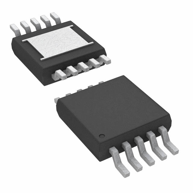
Tiny Thermally Enhanced Leadless (3mm × 3mm)
DFN and 10-lead MSOP Packages
Optional Burst Mode operation provides high efficiency
operation at light loads. 100% duty cycle provides low
dropout operation, extending operating time in batterypowered systems. Burst Mode is inhibited when the MODE
pin is pulled low to reduce noise and RF interference.
The LTC3809-1 allows either coincident or ratiometric
output voltage tracking. Switching frequency is fixed at
550kHz. Fault protection is provided by an overvoltage
comparator and a short-circuit current limit comparator.
The LTC3809-1 is available in tiny footprint thermally
enhanced DFN and 10-lead MSOP packages.
APPLICATIONS
n
n
n
n
, LT, LTC and LTM are registered trademarks of Linear Technology Corporation. Burst
is a registered trademark of Linear Technology Corporation. No RSENSE is a trademark of
Linear Technology Corporation. All other trademarks are the property of their respective
owners. Protected by U.S. Patents including 5481178, 5929620, 6580258, 6304066,
5847554, 6611131, 6498466. Other Patents pending.
1- or 2-Cell Lithium-Ion Powered Devices
Notebook and Palmtop Computers, PDAs
Portable Instruments
Distributed DC Power Systems
TYPICAL APPLICATION
Efficiency and Power Loss vs Load Current
High Efficiency, 550kHz Step-Down Converter
100
10μF
15k
187k
TG
LTC3809-1
470pF
2.2μH
VFB
SW
ITH
BG
VOUT
2.5V
2A
EFFICIENCY (%)
59k
VIN = 5V
1k
VIN = 4.2V
80
100
TYPICAL POWER
LOSS (VIN = 4.2V)
70
10
47μF
RUN
60
1
GND
38091 TA01
POWER LOSS (mW)
MODE
VIN = 3.3V
90
VIN
IPRG
10k
EFFICIENCY
VIN
2.75V TO 9.8V
FIGURE 8 CIRCUIT
VOUT = 2.5V
50
1
10
100
1k
LOAD CURRENT (mA)
0.1
10k
38091 TA02
38091fc
1
�LTC3809-1
ABSOLUTE MAXIMUM RATINGS
(Note 1)
Input Supply Voltage (VIN) ........................ –0.3V to 10V
RUN, TRACK/SS, MODE,
IPRG Voltages ............................... –0.3V to (VIN + 0.3V)
VFB, ITH Voltages ...................................... –0.3V to 2.4V
SW Voltage ......................... –2V to VIN + 1V (10V Max)
TG, BG Peak Output Current (
5V) may work fine at lower voltages (e.g., 3.3V).
Selecting the N-channel MOSFET is typically easier, since
for a given RDS(ON), the gate charge and turn-on and turn-off
delays are much smaller than for a P-channel MOSFET.
Inductor Value Calculation
Given the desired input and output voltages, the inductor
value and operating frequency, fOSC , directly determine
the inductor’s peak-to-peak ripple current:
IRIPPLE =
VOUT VIN – VOUT
•
VIN
fOSC • L
Lower ripple current reduces core losses in the inductor,
ESR losses in the output capacitors and output voltage
ripple. Thus, highest efficiency operation is obtained at
low frequency with a small ripple current. Achieving this,
however, requires a large inductor.
A reasonable starting point is to choose a ripple current
that is about 40% of IOUT(MAX). Note that the largest ripple
current occurs at the highest input voltage. To guarantee
that ripple current does not exceed a specified maximum,
the inductor should be chosen according to:
L≥
VIN – VOUT VOUT
•
fOSC • IRIPPLE VIN
Burst Mode Operation Considerations
The choice of RDS(ON) and inductor value also determines
the load current at which the LTC3809-1 enters Burst Mode
operation. When bursting, the controller clamps the peak
inductor current to approximately:
1 ΔVSENSE(MAX )
IBURST(PEAK ) = •
4
RDS(ON)
The corresponding average current depends on the
amount of ripple current. Lower inductor values (higher
IRIPPLE) will reduce the load current at which Burst Mode
operation begins.
The ripple current is normally set so that the inductor current
is continuous during the burst periods. Therefore,
IRIPPLE ≤ IBURST(PEAK)
This implies a minimum inductance of:
L MIN ≤
VIN – VOUT
V
• OUT
fOSC • IBURST(PEAK ) VIN
A smaller value than LMIN could be used in the circuit,
although the inductor current will not be continuous
during burst periods, which will result in slightly lower
efficiency. In general, though, it is a good idea to keep
IRIPPLE comparable to IBURST(PEAK).
Inductor Core Selection
Once the value of L is known, the type of inductor must be
selected. Actual core loss is independent of core size for a
fixed inductor value, but is very dependent on the inductance selected. As inductance increases, core losses go
down. Unfortunately, increased inductance requires more
turns of wire and therefore copper losses will increase.
Ferrite designs have very low core losses and are preferred at high switching frequencies, so design goals can
concentrate on copper loss and preventing saturation.
Ferrite core material saturates “hard”, which means that
inductance collapses abruptly when the peak design current
is exceeded. Core saturation results in an abrupt increase
in inductor ripple current and consequent output voltage
ripple. Do not allow the core to saturate!
38091fc
14
�LTC3809-1
APPLICATIONS INFORMATION
Different core materials and shapes will change the size/
current and price/current relationship of an inductor. Toroid
or shielded pot cores in ferrite or permalloy materials are
small and don’t radiate much energy, but generally cost
more than powdered iron core inductors with similar
characteristics. The choice of which style inductor to use
mainly depends on the price vs size requirements and any
radiated field/EMI requirements. New designs for surface
mount inductors are available from Coiltronics, Coilcraft,
Toko and Sumida.
Schottky Diode Selection (Optional)
The schottky diode D in Figure 9 conducts current during the dead time between the conduction of the power
MOSFETs. This prevents the body diode of the bottom
N-channel MOSFET from turning on and storing charge
during the dead time, which could cost as much as 1%
in efficiency. A 1A Schottky diode is generally a good
size for most LTC3809-1 applications, since it conducts
a relatively small average current. Larger diode results
in additional transition losses due to its larger junction
capacitance. This diode may be omitted if the efficiency
loss can be tolerated.
CIN and COUT Selection
In continuous mode, the source current of the P-channel
MOSFET is a square wave of duty cycle (VOUT /VIN). To
prevent large voltage transients, a low ESR input capacitor
sized for the maximum RMS current must be used. The
maximum RMS capacitor current is given by:
VOUT • ( VIN – VOUT )
1/ 2
CIN Re quiredIRMS ≈ IMAX •
VIN
This formula has a maximum value at VIN = 2VOUT, where
IRMS = IOUT /2. This simple worst-case condition is commonly used for design because even significant deviations
do not offer much relief. Note that capacitor manufacturer’s
ripple current ratings are often based on 2000 hours of life.
This makes it advisable to further derate the capacitor or
to choose a capacitor rated at a higher temperature than
required. Several capacitors may be paralleled to meet the
size or height requirements in the design. Due to the high
operating frequency of the LTC3809-1, ceramic capacitors
can also be used for CIN. Always consult the manufacturer
if there is any question.
The selection of COUT is driven by the effective series
resistance (ESR). Typically, once the ESR requirement
is satisfied, the capacitance is adequate for filtering. The
output ripple (ΔVOUT) is approximated by:
⎛
⎞
1
ΔVOUT ≈ IRIPPLE • ⎜ ESR +
⎟
8 • f • COUT ⎠
⎝
where f is the operating frequency, COUT is the output
capacitance and IRIPPLE is the ripple current in the inductor. The output ripple is highest at maximum input voltage
since IRIPPLE increase with input voltage.
Setting Output Voltage
The LTC3809-1 output voltage is set by an external
feedback resistor divider carefully placed across the
output, as shown in Figure 3. The regulated output voltage
is determined by:
⎛ R ⎞
VOUT = 0.6 V • ⎜ 1 + B ⎟
⎝ RA ⎠
38091fc
15
�LTC3809-1
APPLICATIONS INFORMATION
For most applications, a 59k resistor is suggested for RA.
In applications where minimizing the quiescent current is
critical, RA should be made bigger to limit the feedback
divider current. If RB then results in very high impedance,
it may be beneficial to bypass RB with a 50pF to 100pF
capacitor CFF.
VOUT
LTC3809-1
RB
CFF
Once the controller is enabled, the start-up of VOUT is controlled by the state of the TRACK/SS pin. If the TRACK/SS
pin is connected to VIN, the start-up of VOUT is controlled
by internal soft-start, which slowly ramps the positive
reference to the error amplifier from 0V to 0.6V, allowing
VOUT to rise smoothly from 0V to its final value. The default
internal soft-start time is around 0.74ms. The soft-start
time can be changed by placing a capacitor between the
TRACK/SS pin and GND. In this case, the soft-start time
will be approximately:
VFB
tSS = CSS •
RA
38091 F03
600mV
1μA
where 1μA is an internal current source which is always on.
Figure 3. Setting Output Voltage
Run and Soft-Start/Tracking Functions
The LTC3809-1 has a low power shutdown mode which is
controlled by the RUN pin. Pulling the RUN pin below 1.1V
puts the LTC3809-1 into a low quiescent current shutdown
mode (IQ = 9μA). Releasing the RUN pin, an internal 0.7μA
(at VIN = 4.2V) current source will pull the RUN pin up
to VIN, which enables the controller. The RUN pin can be
driven directly from logic as showed in Figure 4.
When the voltage on the TRACK/SS pin is less than the
internal 0.6V reference, the LTC3809-1 regulates the VFB
voltage to the TRACK/SS pin voltage instead of 0.6V.
Therefore the start-up of VOUT can ratiometrically track
an external voltage VX, according to a ratio set by a resistor divider at TRACK/SS pin (Figure 5a). The ratiometric
relation between VOUT and VX is (Figure 5c):
VOUT R TA R A + RB
=
•
VX
R A R TA + R TB
VOUT
VX
3.3V OR 5V
LTC3809-1
LTC3809-1
RUN
LTC3809-1
RUN
RTB
TRACK/SS
38091 F04
RB
VFB
RA
RTA
38091 F5a
Figure 4. RUN Pin Interfacing
Figure 5a. Using the TRACK/SS Pin to Track VX
38091fc
16
�LTC3809-1
APPLICATIONS INFORMATION
VOUT
VX
OUTPUT VOLTAGE
OUTPUT VOLTAGE
VX
VOUT
38091 F05b,c
TIME
TIME
(5b) Coincident Tracking
(5c) Ratiometric Tracking
Figure 5b and 5c. Two Different Modes of Output Voltage Tracking
For coincident tracking (VOUT = VX during start-up),
RTA = RA, RTB = RB
VX should always be greater than VOUT when using the
tracking function of TRACK/SS pin.
The internal current source (1μA), which is for external
soft-start, will cause a tracking error at VOUT. For example,
if a 59k resistor is chosen for RTA, the RTA current will be
about 10μA (600mV/59k). In this case, the 1μA internal
current source will cause about 10% (1μA/10μA • 100%)
tracking error, which is about 60mV (600mV • 10%)
referred to VFB. This is acceptable for most applications.
If a better tracking accuracy is required, the value of RTA
should be reduced.
Table 1 summarizes the different states in which the
TRACK/SS can be used.
Table 1. The States of the TRACK/SS Pin
TRACK/SS Pin
FREQUENCY
Capacitor CSS
External Soft-Start
VIN
Internal Soft-Start
Resistor Divider
VOUT Tracking an External Voltage VX
Auxiliary Winding Control Using the MODE Pin
The MODE pin can be used as an auxiliary feedback to
provide a means of regulating a flyback winding output.
When this pin drops below its ground-referenced 0.4V
threshold, continuous mode operation is forced.
During continuous mode, current flows continuously in
the transformer primary side. The auxiliary winding draws
current only when the bottom synchronous N-channel
MOSFET is on. When primary load currents are low and/
or the VIN /VOUT ratio is close to unity, the synchronous
MOSFET may not be on for a sufficient amount of time to
transfer power from the output capacitor to the auxiliary
load. Forced continuous operation will support an auxiliary
winding as long as there is a sufficient synchronous
MOSFET duty factor. The MODE input pin removes
the requirement that power must be drawn from the
transformer primary side in order to extract power from
the auxiliary winding. With the loop in continuous mode,
the auxiliary output may nominally be loaded without
regard to the primary output load.
38091fc
17
�LTC3809-1
APPLICATIONS INFORMATION
The auxiliary output voltage VAUX is normally set, as shown
in Figure 6, by the turns ratio N of the transformer:
VAUX = (N + 1) • VOUT
LTC3809-1
R6
TG
MODE
L1
1:N
VAUX
+
1μF
VOUT
SW
R5
+
BG
COUT
38091 F06
Figure 6. Auxiliary Output Loop Connection
However, if the controller goes into pulse-skipping operation
and halts switching due to a light primary load current, then
VAUX will droop. An external resistor divider from VAUX to
the MODE sets a minimum voltage VAUX(MIN):
⎛ R6 ⎞
VAUX(MIN) = 0.4 V • ⎜ 1 + ⎟
⎝ R5 ⎠
If VAUX drops below this value, the MODE voltage forces
temporary continuous switching operation until VAUX is
again above its minimum.
Fault Condition: Short-Circuit and Current Limit
If the LTC3809-1’s load current exceeds the short-circuit
current limit (ISC), which is set by the short-circuit sense
threshold (ΔVSC) and the on resistance (RDS(ON)) of
bottom N-channel MOSFET, the top P-channel MOSFET
is turned off and will not be turned on at the next clock
cycle unless the load current decreases below ISC. In this
case, the controller’s switching frequency is decreased
and the output is regulated by short-circuit (current limit)
protection.
105
NORMALIZED VOLTAGE OR CURRENT (%)
VIN
In a hard short (VOUT = 0V), the top P-channel MOSFET
is turned off and kept off until the short-circuit condition
is cleared. In this case, there is no current path from
input supply (VIN) to either VOUT or GND, which prevents
excessive MOSFET and inductor heating.
100
VREF
95
MAXIMUM
SENSE VOLTAGE
90
85
80
75
2.0 2.1 2.2 2.3 2.4 2.5 2.6 2.7 2.8 2.9 3.0
INPUT VOLTAGE (V)
38091 F07
Figure 7. Line Regulation of VREF and Maximum Sense Voltage
Low Supply Voltage
Although the LTC3809-1 can function down to below 2.4V,
the maximum allowable output current is reduced as VIN
decreases below 3V. Figure 7 shows the amount of change
as the supply is reduced down to 2.4V. Also shown is the
effect on VREF.
Minimum On-Time Considerations
Minimum on-time, tON(MIN) is the smallest amount of time
that the LTC3809-1 is capable of turning the top P-channel
MOSFET on. It is determined by internal timing delays and
the gate charge required to turn on the top MOSFET. Low
duty cycle and high frequency applications may approach
the minimum on-time limit and care should be taken to
ensure that:
tON(MIN) <
VOUT
fOSC • VIN
38091fc
18
�LTC3809-1
APPLICATIONS INFORMATION
If the duty cycle falls below what can be accommodated
by the minimum on-time, the LTC3809-1 will begin to skip
cycles (unless forced continuous mode is selected). The
output voltage will continue to be regulated, but the ripple
current and ripple voltage will increase. The minimum ontime for the LTC3809-1 is typically about 210ns. However,
as the peak sense voltage (IL(PEAK) • RDS(ON)) decreases,
the minimum on-time gradually increases up to about
260ns. This is of particular concern in forced continuous
applications with low ripple current at light loads. If forced
continuous mode is selected and the duty cycle falls below
the minimum on time requirement, the output will be
regulated by overvoltage protection.
Efficiency Considerations
The efficiency of a switching regulator is equal to the output
power divided by the input power times 100%. It is often
useful to analyze individual losses to determine what is
limiting efficiency and which change would produce the
most improvement. Efficiency can be expressed as:
Efficiency = 100% – (L1 + L2 + L3 + …)
where L1, L2, etc. are the individual losses as a percentage
of input power.
Although all dissipative elements in the circuit produce
losses, four main sources usually account for most of
the losses in LTC3809-1 circuits: 1) LTC3809-1 DC bias
current, 2) MOSFET gate-charge current, 3) I2R losses
and 4) transition losses.
1) The VIN (pin) current is the DC supply current, given
in the Electrical Characteristics, which excludes MOSFET
driver currents. VIN current results in a small loss that
increases with VIN.
2) MOSFET gate-charge current results from switching
the gate capacitance of the power MOSFET. Each time a
MOSFET gate is switched from low to high to low again,
a packet of charge dQ moves from VIN to ground. The
resulting dQ/dt is a current out of VIN, which is typically
much larger than the DC supply current. In continuous
mode, IGATECHG = f • QP.
3) I2R losses are calculated from the DC resistances of the
MOSFETs, inductor and/or sense resistor. In continuous
mode, the average output current flows through L but
is “chopped” between the top P-channel MOSFET and
the bottom N-channel MOSFET. The MOSFET RDS(ON)
multiplied by duty cycle can be summed with the resistance
of L to obtain I2R losses.
4) Transition losses apply to the external MOSFET and
increase with higher operating frequencies and input
voltages. Transition losses can be estimated from:
Transition Loss = 2 • VIN2 • IO(MAX) • CRSS • f
Other losses, including CIN and COUT ESR dissipative losses
and inductor core losses, generally account for less than
2% total additional loss.
Checking Transient Response
The regulator loop response can be checked by looking
at the load transient response. Switching regulators take
several cycles to respond to a step in load current. When
a load step occurs, VOUT immediately shifts by an amount
equal to (ΔILOAD) • (ESR), where ESR is the effective series resistance of COUT. ΔILOAD also begins to charge or
discharge COUT generating a feedback error signal used
by the regulator to return VOUT to its steady-state value.
During this recovery time, VOUT can be monitored for
overshoot or ringing that would indicate a stability problem.
OPTI-LOOP compensation allows the transient response
to be optimized over a wide range of output capacitance
and ESR values.
The ITH series RC-CC filter (see Functional Diagram) sets
the dominant pole-zero loop compensation.
The ITH external components showed in the figure on the
first page of this data sheet will provide adequate compensation for most applications. The values can be modified
slightly (from 0.2 to 5 times their suggested values) to
optimize transient response once the final PC layout is done
and the particular output capacitor type and value have
been determined. The output capacitor needs to be decided
upon because the various types and values determine the
loop feedback factor gain and phase. An output current
38091fc
19
�LTC3809-1
APPLICATIONS INFORMATION
pulse of 20% to 100% of full load current having a rise
time of 1μs to 10μs will produce output voltage and ITH
pin waveforms that will give a sense of the overall loop
stability. The gain of the loop will be increased by increasing RC and the bandwidth of the loop will be increased
by decreasing CC. The output voltage settling behavior is
related to the stability of the closed-loop system and will
demonstrate the actual overall supply performance. For
a detailed explanation of optimizing the compensation
components, including a review of control loop theory,
refer to Application Note 76.
A second, more severe transient is caused by switching
in loads with large (>1μF) supply bypass capacitors. The
discharged bypass capacitors are effectively put in parallel
with COUT, causing a rapid drop in VOUT. No regulator can
deliver enough current to prevent this problem if the load
switch resistance is low and it is driven quickly. The only
solution is to limit the rise time of the switch drive so that
the load rise time is limited to approximately (25) • (CLOAD).
Thus a 10μF capacitor would be require a 250μs rise time,
limiting the charging current to about 200mA.
Design Example
As a design example, assume VIN will be operating from a
maximum of 4.2V down to a minimum of 2.75V (powered
by a single lithium-ion battery). Load current requirement
is a maximum of 2A, but most of the time it will be in a
standby mode requiring only 2mA. Efficiency at both low
and high load currents is important. Burst Mode operation
at light loads is desired. Output voltage is 1.8V. The IPRG
pin will be left floating, so the maximum current sense
threshold ΔVSENSE(MAX) is approximately 125mV.
Maximum Duty Cycle =
VOUT
= 65.5%
VIN(MIN)
From Figure 1, SF = 82%.
ΔVSENSE(MAX )
5
RDS(ON)MAX = • 0.9 • SF •
= 0.032Ω
6
IOUT(MAX ) • ρT
A 0.032Ω P-channel MOSFET in Si7540DP is close to
this value.
The N-channel MOSFET in Si7540DP has 0.017Ω RDS(ON).
The short-circuit current is:
ISC =
90mV
= 5.3A
0.017Ω
So the inductor current rating should be higher than 5.3A.
The LTC3809-1 operates at a frequency of 550kHz. For
continuous Burst Mode operation with 600mA IRIPPLE,
the required minimum inductor value is:
LMIN =
⎛
1.8 V
1.8 V ⎞
• ⎜ 1−
⎟ = 1.88μH
550kHz • 600mA ⎝ 2.75V ⎠
A 6A 2.2μH inductor works well for this application.
CIN will require an RMS current rating of at least 1A
at temperature. A COUT with 0.1Ω ESR will cause
approximately 60mV output ripple.
PC Board Layout Checklist
When laying out the printed circuit board, use the following
checklist to ensure proper operation of the LTC3809-1.
• The power loop (input capacitor, MOSFET, inductor,
output capacitor) should be as small as possible and
isolated as much as possible from LTC3809-1.
• Put the feedback resistors close to the VFB pins. The ITH
compensation components should also be very close
to the LTC3809-1.
• The current sense traces should be Kelvin connections
right at the P-channel MOSFET source and drain.
• Keeping the switch node (SW) and the gate driver nodes
(TG, BG) away from the small-signal components,
especially the feedback resistors, and ITH compensation
components.
38091fc
20
�LTC3809-1
TYPICAL APPLICATIONS
VIN
2.75V TO 8V
1
10μF
MODE
VIN
6
CITH
220pF RITH
15k
4
2
187k
IPRG
TG
LTC3809EDD-1
ITH
SW
TRACK/SS
BG
9
8
MP
Si7540DP
L
1.5μH
10
7
VOUT
2.5V
(5A AT 5VIN)
MN
Si7540DP
3
VFB
GND
RUN
5
COUT
150μF
+
11
59k
100pF
38091 F08
L: VISHAY IHLP-2525CZ-01
COUT: SANYO 4TPB150MC
Figure 8. 550kHz, Synchronous DC/DC Converter with Internal Soft-Start
VIN
2.75V TO 8V
10μF
1
MODE
VIN
6
470pF
15k
4
IPRG
TG
LTC3809EDD-1
ITH
SW
TRACK/SS
BG
9
8
MP
Si3447BDV
L
1.5μH
10
VOUT
1.8V
2A
10nF
2
118k
3
59k
VFB
GND
11
RUN
7
MN
Si3460DV
5
D
(OPT)
COUT
22μF
x2
100pF
L: VISHAY IHLP-2525CZ-01
D: ON SEMI MBRM120LT3 (OPTIONAL)
38091 F09
Figure 9. 550kHz, Synchronous DC/DC Converter with External Soft-Start, Ceramic Output Capacitor
38091fc
21
�LTC3809-1
TYPICAL APPLICATIONS
Synchronous DC/DC Converter with Output Tracking
1
VIN
2.75V TO 8V
10μF
MODE
VIN
6
220pF
15k
4
1.18k
2
Vx
IPRG
TG
LTC3809EDD-1
ITH
SW
TRACK/SS
BG
9
8
MP
Si7540DP
L
1.5μH
10
7
MN
Si7540DP
590Ω
118k
3
VFB
GND
RUN
5
COUT
150μF
VOUT
1.8V
(5A AT 5VIN)
+
11
59k
100pF
38091 TA03
L: VISHAY IHLP-2525CZ-01
COUT: SANYO 4TPB150MC
VOUT < Vx
PACKAGE DESCRIPTION
DD Package
10-Lead Plastic DFN (3mm × 3mm)
(Reference LTC DWG # 05-08-1698)
R = 0.115
TYP
6
0.38 p 0.10
10
0.675 p0.05
3.50 p0.05
1.65 p0.05
2.15 p0.05 (2 SIDES)
3.00 p0.10
(4 SIDES)
PACKAGE
OUTLINE
1.65 p 0.10
(2 SIDES)
PIN 1
TOP MARK
(SEE NOTE 6)
(DD10) DFN 1103
5
0.200 REF
0.25 p 0.05
0.50
BSC
2.38 p0.05
(2 SIDES)
1
0.25 p 0.05
0.50 BSC
0.75 p0.05
0.00 – 0.05
2.38 p0.10
(2 SIDES)
BOTTOM VIEW—EXPOSED PAD
RECOMMENDED SOLDER PAD PITCH AND DIMENSIONS
NOTE:
1. DRAWING TO BE MADE A JEDEC PACKAGE OUTLINE M0-229 VARIATION
OF (WEED-2). CHECK THE LTC WEBSITE DATA SHEET FOR CURRENT STATUS
OF VARIATION ASSIGNMENT
2. DRAWING NOT TO SCALE
3. ALL DIMENSIONS ARE IN MILLIMETERS
4. DIMENSIONS OF EXPOSED PAD ON BOTTOM OF PACKAGE DO NOT INCLUDE
MOLD FLASH. MOLD FLASH, IF PRESENT, SHALL NOT EXCEED 0.15mm ON
ANY SIDE
5. EXPOSED PAD SHALL BE SOLDER PLATED
6. SHADED AREA IS ONLY A REFERENCE FOR PIN 1 LOCATION ON THE
TOP AND BOTTOM OF PACKAGE
38091fc
22
�LTC3809-1
PACKAGE DESCRIPTION
MSE Package
10-Lead Plastic MSOP, Exposed Die Pad
(Reference LTC DWG # 05-08-1664 Rev C)
BOTTOM VIEW OF
EXPOSED PAD OPTION
2.794 p 0.102
(.110 p .004)
5.23
(.206)
MIN
0.889 p 0.127
(.035 p .005)
1
0.05 REF
10
DETAIL “B”
CORNER TAIL IS PART OF
DETAIL “B” THE LEADFRAME FEATURE.
FOR REFERENCE ONLY
NO MEASUREMENT PURPOSE
3.00 p 0.102
(.118 p .004)
(NOTE 3)
10 9 8 7 6
DETAIL “A”
0o – 6o TYP
1 2 3 4 5
GAUGE PLANE
0.53 p 0.152
(.021 p .006)
DETAIL “A”
0.18
(.007)
0.497 p 0.076
(.0196 p .003)
REF
3.00 p 0.102
(.118 p .004)
(NOTE 4)
4.90 p 0.152
(.193 p .006)
0.254
(.010)
0.29
REF
1.83 p 0.102
(.072 p .004)
2.083 p 0.102 3.20 – 3.45
(.082 p .004) (.126 – .136)
0.50
0.305 p 0.038
(.0197)
(.0120 p .0015)
BSC
TYP
RECOMMENDED SOLDER PAD LAYOUT
2.06 p 0.102
(.081 p .004)
SEATING
PLANE
0.86
(.034)
REF
1.10
(.043)
MAX
0.17 – 0.27
(.007 – .011)
TYP
0.50
(.0197)
BSC
0.1016 p 0.0508
(.004 p .002)
MSOP (MSE) 0908 REV C
NOTE:
1. DIMENSIONS IN MILLIMETER/(INCH)
2. DRAWING NOT TO SCALE
3. DIMENSION DOES NOT INCLUDE MOLD FLASH, PROTRUSIONS OR GATE BURRS.
MOLD FLASH, PROTRUSIONS OR GATE BURRS SHALL NOT EXCEED 0.152mm (.006") PER SIDE
4. DIMENSION DOES NOT INCLUDE INTERLEAD FLASH OR PROTRUSIONS.
INTERLEAD FLASH OR PROTRUSIONS SHALL NOT EXCEED 0.152mm (.006") PER SIDE
5. LEAD COPLANARITY (BOTTOM OF LEADS AFTER FORMING) SHALL BE 0.102mm (.004") MAX
38091fc
Information furnished by Linear Technology Corporation is believed to be accurate and reliable.
However, no responsibility is assumed for its use. Linear Technology Corporation makes no representation that the interconnection of its circuits as described herein will not infringe on existing patent rights.
23
�LTC3809-1
RELATED PARTS
PART NUMBER
DESCRIPTION
COMMENTS
LTC1628/LTC3728
Dual High Efficiency, 2-Phase Synchronous Step Down Controllers
Constant Frequency, Standby, 5V and 3.3V LDOs, VIN to 36V,
LTC1735
High Efficiency Synchronous Step-Down Controller
Burst Mode Operation, 16-Pin Narrow SSOP, Fault Protection,
3.5V ≤ VIN ≤ 36V
LTC1773
Synchronous Step-Down Controller
2.65V ≤ VIN ≤ 8.5V, IOUT Up to 4A, 10-Lead MSOP
LTC1778
No RSENSE , Synchronous Step-Down Controller
Current Mode Operation Without Sense Resistor,
Fast Transient Response, 4V ≤ VIN ≤ 36V
LTC1872
Constant Frequency Current Mode Step-Up Controller
2.5V ≤ VIN ≤ 9.8V, SOT-23 Package, 550kHz
LTC3411
1.25A (IOUT), 4MHz, Synchronous Step-Down DC/DC Converter
95% Efficiency, VIN: 2.5V to 5.5V, VOUT = 0.8V, IQ = 60μA,
ISD =


 工商网监
湘ICP备2023018690号
工商网监
湘ICP备2023018690号
