LTC4110
Battery Backup
System Manager
FEATURES
DESCRIPTION
n
The LTC®4110 is a complete single chip, high efficiency,
flyback battery charge and discharge manager with automatic switchover between the input supply and the backup
battery or super capacitor. The IC provides four modes of
operation: battery backup, battery charge, battery calibration and shutdown. Battery backup and battery charge are
automatic standalone modes, while the optional calibration
mode requires a CPU host to communicate over an SMBus.
During calibration the flyback charger is used in reverse
to discharge the battery with a programmable constant
current into the system load eliminating heat generation.
Three status outputs can be individually reconfigured over
the SMBus to become GPIOs. User programmable overdischarge protection is provided. The SHDN pin isolates
the battery to support shipping the product with a charged
battery installed.
n
n
n
n
n
n
n
n
n
n
n
n
n
Complete Backup Battery Manager for Li-Ion/
Polymer, Lead Acid, NiMH/NiCd Batteries and
Super Capacitors
Charge and Discharge Battery with Voltages Above
and Below the Input Supply Voltage
“No Heat” Battery Calibration Discharge Using
System Load
Automatic Battery Backup with Input Supply
Removal Using PowerPath™ Control
Standalone for Li-Ion/Polymer, SLA, and Supercaps
Optional SMBus/I2C Support Allows Battery
Capacity Calibration Operation with Host
Over- and Under-Battery Voltage Protection
Adjustable Battery Float Voltage
Precision Charge Voltage ±0.5%
Programmable Charge/Calibration Current Up to
3A with ±3% Accuracy
Optional Temperature Qualified Charging
Wide Backup Battery Supply Range: 2.7V to 19V
Wide Input Supply Range: 4.5V to 19V
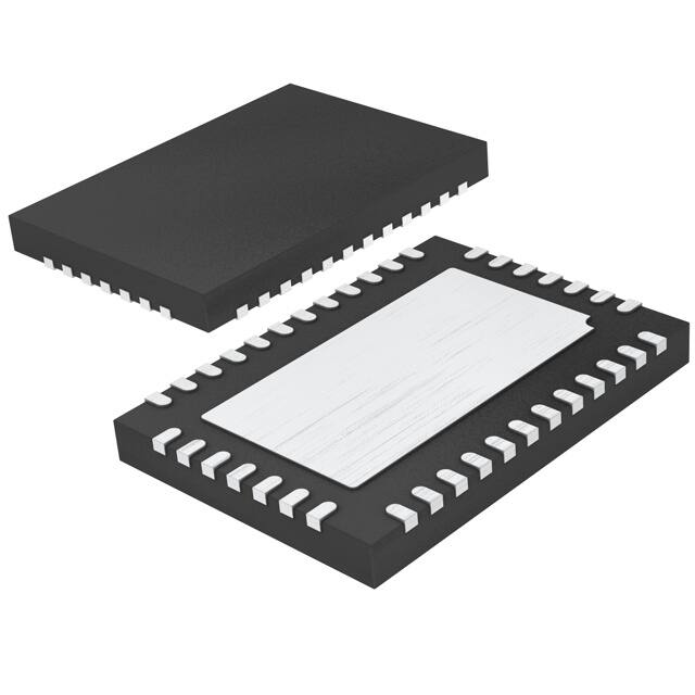
38-Lead (5mm × 7mm) QFN Package
APPLICATIONS
n
n
n
n
Multiple LTC4110s can be combined to form a redundant
battery backup system or increase the number of battery
packs to achieve longer backup run times.
The LTC4110 is available in a low profile (0.75mm), 38-pin
5mm × 7mm QFN package. The QFN features an exposed
metal die mount pad for optimum thermal performance.
L, LT, LTC and LTM are registered trademarks of Linear Technology Corporation. PowerPath
is a trademark of Linear Technology Corporation. All other trademarks are the property of their
respective owners.
Backup Battery Systems
Server Memory Backup
Medical Equipment
High Reliability Systems
TYPICAL APPLICATION
Battery Backup System Manager
SYSTEM LOAD
Server Backup System (In Backup Mode)
BACKUP LOAD (DCOUT)
SYSTEM LOAD
(DC/DC, ETC.)
CURRENT FLOW
DCIN
0V
OFF
ON
LTC4110
BATTERY
BACKUP
SYSTEM
MANAGER
ON
BATTERY
BACKUP LOAD
(MEMORY, ETC.)
CURRENT FLOW
BATTERY
HOST CPU
INID
UVLO
SET POINT
DCDIV
BATID
LTC4110
I2C BUS
CHGFET
4110 TA01b
DCHFET
4110 F01
4110fb
1
�LTC4110
ABSOLUTE MAXIMUM RATINGS
PIN CONFIGURATION
(Note 1)
DCHFET
CHGFET
VDD
BATID
NC
DCOUT
INID
TOP VIEW
38 37 36 35 34 33 32
DCIN 1
31 BAT
CLN 2
30 SELC
CLP 3
29 ISENSE
ACPDLY 4
28 SGND
27 CSN
DCDIV 5
SHDN 6
26 CSP
39
SDA 7
25 ITH
SCL 8
24 ICHG
GPI01 9
23 ICAL
GPI02 10
22 IPCC
GPI03 11
21 THB
20 THA
SELA 12
TYPE
TIMER
VREF
VCAL
VCHG
VDIS
13 14 15 16 17 18 19
ACPb
DCIN, BAT, DCOUT, DCDIV, SHDN
to GND ....................................................... –0.3V to 20V
Input Voltage (CLP, CLN) ...............–0.3V to DCIN + 0.3V
Input Voltage (CSP, CSN) ................–0.3V to BAT + 0.3V
Input Voltage
(GPIO1, GPIO2, GPIO3, SELC, SELA, TYPE, VCHG,
THA, THB, ISENSE, ACPDLY, SDA, SCL) .... –0.3V to 7V
Input Voltage (VCAL, VDIS) ....................... –0.3V to 1.35V
Output Voltage
(ACPb, GPIO1, GPIO2, GPIO3) ................ –0.3V to 7V
CLP-CLN, CSP-CSN ..................................................±1V
Operating Temperature Range (Note 2)....–40°C to 85°C
Junction Temperature (Note 3) ............................. 105°C
Storage Temperature Range
QFN Package......................................–65°C to 125°C
UHF PACKAGE
38-LEAD (5mm s 7mm) PLASTIC QFN
TJMAX = 100°C, θJA = 34°C/W
EXPOSED PAD (PIN 39) IS GND, MUST BE SOLDERED TO PCB
ORDER INFORMATION
LEAD FREE FINISH
TAPE AND REEL
PART MARKING
PACKAGE DESCRIPTION
TEMPERATURE RANGE
LTC4110EUHF#PBF
LTC4110EUHF#TRPBF
4110
38-Lead (5mm × 7mm) Plastic QFN
–40°C to 85°C
LEAD BASED FINISH
TAPE AND REEL
PART MARKING
PACKAGE DESCRIPTION
TEMPERATURE RANGE
LTC4110EUHF
LTC4110EUHF#TR
4110
38-Lead (5mm × 7mm) Plastic QFN
–40°C to 85°C
Consult LTC Marketing for parts specified with wider operating temperature ranges.
For more information on lead free part marking, go to: http://www.linear.com/leadfree/
For more information on tape and reel specifications, go to: http://www.linear.com/tapeandreel/
4110fb
2
�LTC4110
ELECTRICAL CHARACTERISTICS
The l denotes the specifications which apply over the full operating
temperature range, otherwise specifications are at TA = 25°C. Unless otherwise specified, VDCIN = VDCOUT = VDCDIV = 12V, VBAT = 8.4V,
GND = SGND = CLP = CLN = SHDN = 0V and RVREF = 49.9k. All currents into device pins are positive and all currents out of device pins
are negative. All voltages are referenced to GND, unless otherwise specified.
SYMBOL
PARAMETER
CONDITIONS
MIN
TYP
MAX
UNITS
DCIN
Operating Voltage Range
Charge or Calibration Modes
l
4.5
19
V
DCOUT
Operating Voltage Range
Power Input
Charge or Calibration Modes
l
4.5
19
V
Backup Mode
l
2.7
19
V
Backup Mode
l
2.7
19
V
VBAT
Operating Voltage Range
ISPLY
Supply Current (IDCIN + IDCOUT) in Idle Mode
(Note 4)
2
3
mA
IBIDL
Battery Current in Idle Mode (Notes 4 and 5)
30
45
μA
IBBU
Battery Current in Backup Mode (Note 5)
2
3
mA
VDCIN = 0
IBSD
Battery Current in Shutdown (Note 5)
VSHDN = VBAT , VDCIN = 0
20
45
μA
VUVI
Undervoltage Lockout Exit Threshold
VDCIN Increasing
l
3.7
4
4.45
V
VUVD
Undervoltage Lockout Entry Threshold
VDCIN Decreasing
l
3.4
3.7
4.1
V
VUVH
Undervoltage Lockout Hysteresis
400
mV
VDD Regulator
VDD
Output Voltage
No Load
l
4.5
VDD(MIN)
Output Voltage
IDD = –10mA
l
4.25
4.20V for Li-Ion. 2.35V for Lead Acid (Note 8)
VCHG = GND
–5°C < TA < 85°C (Note10)
l
–40°C < TA < 85°C
–0.5
0.5
%
–0.8
–1
0.8
1
%
%
–2
2
%
–3
3
%
4.75
5
V
V
Charging Performance
VFTOL
Charge Float Voltage Accuracy
VFATOL
Charge Float Voltage Adjust Accuracy
0.3V and –0.3V for Li-Ion Batteries,
0.15V and –0.15V for Lead Acid Batteries
(Note 8)
IBTOL
Bulk Charge Current Accuracy (Note 7)
VCSP – VCSN =100mV
VBAT ≥ 3.1V
–40°C < TA < 85°C
IPTOL
Preconditioning and Wake-Up Current
Accuracy (Note 7)
l
l
–5
5
%
VBAT ≥ 3.3V (Note 8), VCSP – VCSN = 10mV;
Li-Ion and NiMH/NiCd Batteries Only
–30
30
%
VBAT ≤ 3.3 (Note 8), VCSP – VCSN = 10mV;
Li-Ion and NiMH/NiCd Batteries Only
–40
40
%
ISKVA
Voltage Error Amplifier Sink Current at ITH Pin VITH = 2V
96
μA
ISRCA
Current Error Amplifier Source Current at ITH
Pin
VITH = 2V
–24
μA
ISKCA
Current Error Amplifier Sink Current at ITH Pin VITH = 2V
24
μA
IVCHG
VCHG Pin Bias Current
VCHG = 1.25V
–100
VBC
Bulk Charge Threshold Voltage;
VBAT Increasing (Note 8)
Li-Ion, VCHG = GND
NiMH/NiCd
2.80
0.84
VBCH
Bulk Charge Threshold Voltage Hysteresis;
VBAT Decreasing (Note 8)
Li-Ion, VCHG = GND
NiMH/NiCd
VAR
Auto Recharge Threshold Voltage;
VBAT Decreasing
Standard Li-Ion Only;
Specified as Percentage of Float Voltage
VARH
Auto Recharge Threshold Hysteresis Voltage;
VBAT Increasing
Standard Li-Ion Only; Specified as
Percentage of Float Voltage
3.00
0.90
100
nA
3.20
0.96
V
V
85
40
93
95
2
mV
mV
97
%
%
4110fb
3
�LTC4110
ELECTRICAL CHARACTERISTICS
The l denotes the specifications which apply over the full operating
temperature range, otherwise specifications are at TA = 25°C. Unless otherwise specified, VDCIN = VDCOUT = VDCDIV = 12V, VBAT = 8.4V,
GND = SGND = CLP = CLN = SHDN = 0V and RVREF = 49.9k. All currents into device pins are positive and all currents out of device pins
are negative. All voltages are referenced to GND, unless otherwise specified.
SYMBOL
PARAMETER
CONDITIONS
MIN
TYP
MAX
UNITS
VBOV
Battery Overvoltage Threshold;
VBAT Increasing
All Li-Ion, Lead Acid as Percentage of
Float Voltage
NiMH/NiCd (Note 8)
105
1.80
107.5
1.85
110
1.90
%
V
Battery Overvoltage Threshold Hysteresis;
VBAT Increasing.
All Li-Ion, Lead Acid as Percentage of
Float Voltage
NiMH/NiCd (Note 8)
VBOVH
VREF
Reference Pin Voltage Range
FTMR
Programmed Timer Accuracy
tTIMEOUT
Time Between Receiving Valid
ChargingCurrent() and ChargingVoltage()
Commands. Wake-Up Timer.
CTIMER = 47nF
2
40
%
mV
l
1.208
1.220
1.232
V
l
–15
0
15
%
l
140
175
210
sec
l
–1.1
–1.3
1.1
1.3
%
%
Calibration Performance
VCTOL
Calibration Cut-Off Default Voltage Accuracy;
VBAT Decreasing
VCTOLH
Calibration Cut-Off Default Voltage Hysteresis; Li-Ion
VBAT Increasing. (Note 8)
Lead Acid
NiMH/NiCd
VCATOL
Calibration Cut-Off Voltage Adjust Accuracy
±400mV for Li-Ion, ±300mV for Lead Acid,
±200mV for NiMH/NiCd (Note 8)
l
IFTOL
Calibration Current Accuracy (Note 7)
VCSP – VCSN = –100mV
l
IVCAL
VCAL Pin Leakage Current
VCAL = 1.25V
IBDT
Back-Drive Current Limit Threshold
VCLP – VCLN Decreasing
VCLN = VDCIN
IBDH
Back-Drive Current Limit Threshold Hysteresis VCLP – VCLN Increasing
VCLN = VDCIN
VOVP
Calibration Mode Input Overvoltage
Comparator DCDIV Pin Threshold
VDCDIV Rising
VOVPH
Calibration Mode Input Overvoltage
Comparator DCDIV Pin Hysteresis
VDCDIV Falling
2.75V for Li-Ion, 1.93V for Lead Acid,
VCAL = GND (Note 8), 0.95V for NiMH/NiCd
85
50
40
l
–1.5
mV
mV
mV
1.5
–5
5
%
–100
100
nA
13
mV
7
10
1
l
%
1.4
1.5
mV
1.6
100
V
mV
AC Present and Discharge Cut-Off Comparators
VAC
AC Present Comparator DCDIV Pin Threshold
VDCDIV Falling
VACH
AC Present Comparator DCDIV Pin Hysteresis
VDCDIV Rising
IAC
AC Present Comparator DCDIV Pin Input Bias
Current
VDCDIV = 1.25V
tAC
ACPb Pin Externally Programmed Falling Delay CACPDLY = 100nF, RVREF = 49.9k,
VDCDIV Stepped From 1.17V to 1.30V
VDTOL
Discharge Cut-Off Default Voltage Accuracy;
VBAT Decreasing
2.75V for Li-Ion, 1.93V for Lead Acid,
VDIS = GND, 0.95V for NiMH/NiCd
VDTOLH
Discharge Cut-Off Default Voltage Hysteresis;
VBAT Increasing (Note 8)
Li-Ion
Lead acid
NiMH/NiCd
VDATOL
Discharge Cut-Off Voltage Adjust Accuracy
±400mV for Li-Ion, ±300mV for Lead Acid,
±200mV for NiMH/NiCd
IVDIS
VDIS Pin Bias Current
VDIS = 1.25V
l
1.196
1.22
1.244
50
8
l
10
–1.5
mV
100
nA
12
ms
1.5
%
85
50
40
l
V
mV
mV
mV
2
2
%
–100
100
nA
4110fb
4
�LTC4110
ELECTRICAL CHARACTERISTICS
The l denotes the specifications which apply over the full operating
temperature range, otherwise specifications are at TA = 25°C. Unless otherwise specified, VDCIN = VDCOUT = VDCDIV = 12V, VBAT = 8.4V,
GND = SGND = CLP = CLN = SHDN = 0V and RVREF = 49.9k. All currents into device pins are positive and all currents out of device pins
are negative. All voltages are referenced to GND, unless otherwise specified.
SYMBOL
PARAMETER
CONDITIONS
MIN
TYP
MAX
UNITS
Input and Battery Ideal Diodes and Switches
VFR
Forward Regulation Voltage (VDCIN -VDCOUT ,
VBAT -VDCOUT)
2.7V ≤ VDCIN ≤ 19V
l
10
20
32
mV
VREV
Reverse Voltage Turn-Off Voltage
(VDCIN-VDCOUT, VBAT -VDCOUT)
2.7V ≤ VDCIN ≤ 19V
l
–30
–18
–8
mV
VGON
“ON” Gate Clamping Voltage (VDCIN -VINID ,
VBAT -VBATID )
IINID , IBATID = 1μA
7
8.3
9.7
V
VGOFF
“OFF” Gate Voltage (VDCIN -VINID, VBAT -VBATID) IINID, IBATID = –10μA
VSHDN = 0V and VDCIN (Shutdown)
0.25
V
VFO
BATID Fast-On Voltage Comparator Threshold
IBATID > 500μA
100
mV
INID Pin Delay Times
CINID = 10nF
DCIN is Switched Between 12.2V and 11.8V
From DCOUT – VGOFF to DCOUT –6V
From DCOUT – VGON to DCOUT –1.5V
450
8
700
20
μs
μs
CBATID = 2.5nF
BAT is Switched Between 12.2V and 11.8V
From DCOUT – VGOFF to DCOUT –6V
From DCOUT – VGON to DCOUT –1.5V
15
8
60
20
μs
μs
4.75
5.25
tIIDON
tIIDOFF
Turn “ON”
Turn “OFF”
BATID Pin Delay Times
tBIDON
tBIDOFF
Turn “ON”
Turn “OFF”
45
PWM Flyback Converter
VOHF
CHGFET, DCHFET High
ICHGFET, IDCHFET = –1mA
VOLF
CHGFET, DCHFET Low
ICHGFET, IDCHFET = 1mA
50
mV
VOLFX
CHGFET, DCHFET in Shutdown and Backup
Modes
VDCIN = VDCDIV = VDCOUT = 0V (Shutdown
Mode), VDCIN = VDCDIV = 0V (Backup Mode)
ICHGFET , IDCHFET = 1μA
100
mV
35
15
65
65
ns
ns
tR
tF
CHGFET, DCHFET Transition Times
Rise Time
Fall Time
FPWM
PWM Oscillator Switching Frequency
4.5
CLOAD = 1.6nF, 20% to 80%
CLOAD = 1.6nF, 20% to 80%
V
l
255
300
340
kHz
SafetySignal Decoder
SafetySignal Trip
(RES_COLD/RES_OR)
RTHA = 1130Ω ±1%, CTH = 1nF (Note 6) RTHB
l
= 54.9k ±1%.
Smart Batteries and Li-Ion Only
95
100
105
k
SafetySignal Decoder
SafetySignal Trip
(RES_IDEAL/RES_COLD)
RTHA = 1130Ω ±1%, CTH = 1nF (Note 6) RTHB
l
= 54.9k ±1%
Smart Batteries and Li-Ion Only
28.5
30
31.5
k
SafetySignal Decoder
SafetySignal Trip
(RES_HOT/RES_IDEAL)
RTHA = 1130Ω ±1%, CTH = 1nF (Note 6) RTHB
l
= 54.9k ±1%
Smart Batteries and Li-Ion Only
2.85
3
3.15
k
SafetySignal Decoder
SafetySignal Trip
(RES_UR/RES_HOT)
RTHA = 1130Ω ±1%, CTH = 1nF (Note 6) RTHB
l
= 54.9k ±1%
Smart Batteries and Li-Ion Only
425
500
575
Ω
VHOT
THB Pin Hot Threshold Voltage
VTHB Decreasing; Lead Acid Only
l
0.28 •
VTHA
0.30 •
VTHA
0.36 •
VTHA
V
VHOTH
THB Pin Hot Threshold Hysteresis Voltage
VTHB Increasing; Lead Acid Only
VREM
THB Pin Battery Removal Threshold Voltage
VTHB Increasing; Lead Acid Only
l
0.90 •
VTHA
0.94 •
VTHA
SafetySignal Decoder and Thermistor Interface
SSOR
SSCLD
SSIDL
SSHOT
50
mV
0.96 •
VTHA
V
4110fb
5
�LTC4110
ELECTRICAL CHARACTERISTICS
The l denotes the specifications which apply over the full operating
temperature range, otherwise specifications are at TA = 25°C. Unless otherwise specified, VDCIN = VDCOUT = VDCDIV = 12V, VBAT = 8.4V,
GND = SGND = CLP = CLN = SHDN = 0V and RVREF = 49.9k. All currents into device pins are positive and all currents out of device pins
are negative. All voltages are referenced to GND, unless otherwise specified.
SYMBOL
PARAMETER
CONDITIONS
MIN
VREMH
THB Pin Battery Removal Threshold
Hysteresis Voltage
VTHB Decreasing; Lead Acid Only
TYP
MAX
25
UNITS
mV
Logic and Status Output Levels
SCL/SDA Input Pins Low Voltage
l
VIHS
SCL/SDA Input Pins High Voltage
l
VOLS
SDA Output Pin Low Voltage
IPULL-UP = 350μA
VOLG
ACPb, GPIO1,2,3 Output Pins Low Voltage
IACPb, IGPIO1, IGPIO2, IGPIO3 = 10mA
IOHG
ACPb, GPIO1,2,3 Output Pins Open
Leakage Current
Outputs Open, VACPb, VGPIO1,2,3 = 5V
VILS
0.8
2.1
V
l
–2
VILG
GPIO Input Low Voltage
l
VIHG
GPIO Input High Voltage
l
VILSD
SHDN Input Pin Low Voltage
VIHSD
SHDN Input Pin High Voltage
IISD
SHDN Input Pin Pull-Up Current
VSHDN = 2.4V
TLR
Logic Reset Duration After Power-Up
From Zero
VDCIN Transition From 0V to 5V in 1V between
the CLP and CLN pins may damage the device.
ACPDLY (Pin 4): ACPb Delay Control Pin. A capacitor
connected from ACPDLY to GND and a resistor from
VREF to GND programs delay in the ACPb pin high-to-low
transition. Open if minimum delay is desired.
DCDIV (Pin 5): AC Present Detection Input. Backup
operation is invoked when the system power voltage,
divided by an external resistor divider, falls below the
threshold of this pin.
SHDN (Pin 6): Active High Shutdown/Reset Control Logic
Input. Forces micropower shutdown mode if high when
DCIN supply is removed. Forces all registers to reset if high
when DCIN supply is present. Normally tied to ground.
Internal pin pull-up current.
SDA (Pin 7): SMBus Bidirectional Data Signal. Connect
to VDD when not in use.
SCL (Pin 8): SMBus Clock Signal Input From SMBus Host.
Connect to VDD when not in use.
GPIO1 (Pin 9): General Purpose I/O or Charge Status Pin. A
logic-level I/O bit port that is configurable as a host-driven
input/output port or as a battery charge status output (CHGb)
with an open-drain N-MOSFET that is asserted low when any
smart battery or Li-Ion battery is in any phase of charging
or when lead acid battery charge current is >C/x where:
C
x=
•5
ICHG
(See C/x Charge Termination section for more details).
If the No SMBus option is selected with the SELA pin,
the GPIO1 pin defaults as battery charge status. Refer
to Table 5a.
GPIO2 (Pin 10): General Purpose I/O Pin. A logic-level I/O bit
port that is configurable as a host-driven input/output port
or as a battery undervoltage status output (BKUP_FLTb)
with an open-drain N-MOSFET that is asserted low only
while in backup mode if the battery’s average cell voltage
drops below voltage programmed by the VDIS pin. If the
No SMBus option is selected with the SELA pin, then the
GPIO2 pin defaults as battery undervoltage status. Refer
to Table 5c.
GPIO3 (Pin 11): General Purpose I/O Pin. A logic-level I/O
bit port that is configurable as a host-driven input/output
port or as a calibration complete status output (CAL_COMPLETEb) with an open-drain N-MOSFET that is asserted
low when calibration has been completed. If the SELA pin
is programmed for no SMBus use then the status output
is charge fault (CHGFLTb) instead of calibration complete.
Refer to Table 5e.
SELA (Pin 12): SMBus Address Selection Input. Selects
the LTC4110 SMBus address to facilitate redundant backup
systems when standard batteries are used. Connect to
GND for 12h, VDD for 28h and the VREF pin for 20h. When
a smart battery is selected by the TYPE pin, the SELA pin
must be connected to GND to select address 12h. If the
SMBus is not used or to force all GPIOs to status mode
upon power-up, connect pin to a typically 0.5 • VREF voltage from VREF pin resistor divider. The SMBus address,
if used, will be 12h.
4110fb
8
�LTC4110
PIN FUNCTIONS
ACPb (Pin 13): AC Present Status Digital Output. OpenDrain N-MOSFET output is asserted low when the main
supply is present as detected by the DCDIV pin and internal
DCIN UVLO.
VDIS (Pin 14): Battery Discharge Voltage Limit During
Backup Program Input. Battery threshold voltage at which
backup mode will terminate by turning off the isolation
P-MOSFET with the BATID pin. Adjustable from external
resistor string biased from VREF pin. For default threshold
connect to GND pin.
VCAL (Pin 15): Battery Voltage Limit During Calibration Program Input. Battery threshold voltage at which
calibration will terminate. Adjustable from external resistor
string biased from VREF pin. For default threshold connect
to GND pin.
VCHG (Pin 16): Battery Float Voltage Program Input. Trims
the float voltage during charging. Programmed from
external resistor string biased from VREF pin. Connect to
GND for default float voltage.
VREF (Pin 17): Voltage Reference Output and Timing Programming Input. Provides a typical virtual reference of 1.220V
(VREF) for an external resistor divider tied between this pin and
GND that programs the VCHG, VCAL and VDIS pin functions.
Total resistance from VREF to GND, along with the capacitor
on the timer pin, programs the charge time. Voltage reference output remains active in all modes except shutdown.
Load current must be between 10μA and 25μA.
TIMER (Pin 18): Charge Timing Input. A capacitor connected between TIMER and GND along with the resistance
connected from VREF to GND programs the charge time
intervals.
TYPE (Pin 19): Refer to Table 8.
THA (Pin 20): SafetySignal Force/Sense Pin to Smart
Battery and Force Pin to Lead Acid Battery Thermistor.
See description of operation for more detail. The maximum allowed combined capacitance on THA, THB and
SafetySignal is 1nF. For lead acid battery applications the
maximum capacitance on the THA pin is 50pF.
THB (Pin 21): SafetySignal Force/Sense Pin to Smart
Battery and Sense Pin to Lead Acid Battery Thermistor.
See description of operation for more detail. The maximum allowed combined capacitance on THA, THB and
SafetySignal is 1nF.
IPCC (Pin 22): Battery Preconditioning Charge Current
Program Input. Programs the battery current during
preconditioning or wakeup charging. Programmed from
external resistor to GND.
ICAL (Pin 23): Battery Discharge Current During Calibration
Program Input. Programs the constant discharge current at
the battery during calibration. Programmed from external
resistor to GND.
ICHG (Pin 24): Battery Current During Charge Program Input.
Programs the battery current while constant-current bulk
charging. Programmed from external resistor to GND.
ITH (Pin 25): Control Signal of the Current Mode PWM. AC
compensates control loop. Higher ITH voltage corresponds
to higher charging current.
CSP (Pin 26): Current Sense Positive Input. This pin and
the CSN pin measure voltage across the external current
sense resistor to control battery current during charging
and calibration.
CSN (Pin 27): Current Sense Negative Input. This pin and
the CSP pin measure voltage across the external current
sense resistor to control battery current during charging
and calibration.
SGND (Pin 28): Signal Ground Reference Input. This pin
should be Kelvin connected to the flyback current sense
resistor and to the battery return.
ISENSE (Pin 29): Current Sense Input. Senses current in
the flyback transformer by monitoring voltage across the
external current sense resistor. This pin should be Kelvinconnected to the resistor.
SELC (Pin 30): Refer to Table 8.
4110fb
9
�LTC4110
PIN FUNCTIONS
BAT (Pin 31): Battery Voltage Sense Input. This pin is used
to monitor the battery and control charging voltage through
an internal resistor divider connected to this pin that is
disconnected in shutdown mode. Also provides a control
input for battery ideal diode functions. Pin should be Kelvinconnected to battery to avoid voltage drop errors.
DCHFET (Pin 32): Drives the Gate of an External N-MOSFET.
Used to drive energy into the battery side of the high efficiency switch mode converter during low loss calibration
discharge of the battery. Provides synchronous rectification
during battery charging.
CHGFET (Pin 33): Drives the Gate of an External NMOSFET. Used to drive energy into the supply side of
the high efficiency switch mode converter during battery
charging. Provides synchronous rectification during low
loss calibration mode.
BATID (Pin 35): Drives the Gate of the Battery P-MOSFET
Ideal Diode. Controls low loss ideal diode between the
battery and backup load when in backup mode. When not
in backup mode, the P-MOSFET is turned off to prevent
battery power from back driving into main power.
NC (Pin 36): No Connect.
DCOUT (Pin 37): System Power Output Voltage Monitor
Input. Provides a control input for supply input ideal diode
and battery ideal diode functions. Also supplies power to the
IC. Bypass at pin with 100nF low ESR capacitor to GND.
INID (Pin 38): Drives the Gate of the Supply Input P-MOSFET
Ideal Diode. Controls low loss ideal diode between the supply input and backup load when not in backup mode.
Exposed Pad (Pin 39): Ground. The Exposed Pad must
be soldered to the PCB.
VDD (Pin 34): Bypass Capacitor Connection for Internal
VDD Regulator. Bypass at pin with 100nF low ESR capacitor to GND.
4110fb
10
�LTC4110
BLOCK DIAGRAM
37 DCOUT
36 NC
SUPPLY INPUT BATTERY
PowerPath CONTROLLER
INID 38
35 BATID
DCIN 1
31 BAT
VDD 34
VDD
REGULATOR
NUMBER
OF CELLS
CA
+
–
GND 39
27 CSN
26 CSP
PRECISION
VOLTAGE DIVIDER
CHG/DCH
SWITCH
CURRENT
SELECTION
22 IPCC
+
–
EA
CLP 3
CURRENT
SWITCH
1.220
23 ICAL
CLN 2
25 ITH
DCDIV 5
VREF 17
VCHG 16
24 ICHG
VOLTAGE REFERENCE
ANALOG COMPARATORS
AND SWITCHES
÷10
33 CHGFET
–
+
PWM
LOGIC
VCAL 15
32 DCHFET
VDIS 14
29 ISENSE
SELC 30
PROGRAMMING CURRENT
OSC
TYPE 19
28 SGND
18 TIMER
4 ACPDLY
SHDN 6
UVLO
SDA 7
SCL 8
SMBus
INTERFACE
AND CONTROL
SELA 12
13 ACPb
TIMER/
CONTROLLER
9 GPIO1
THA 20
THB 21
THERMISTOR
INTERFACE
10 GPIO2
11 GPIO3
4110 BD
4110fb
11
�LTC4110
OPERATION
OVERVIEW
In the typical application, the LTC4110 is placed in series
with main power supply that powers all or part of the
system, which must include the device(s) or system that
needs battery backup.
The LTC4110 has four modes of operation:
• Battery Backup Mode
• Battery Charge Mode
• Battery Calibration Mode
• Shutdown Mode
The LTC4110 provides complete PowerPath control for
the battery backed up load switching automatically from
the main power supply to the battery when battery backup
mode is required. Low loss ideal diode FET switches are
used to connect the main supply or the battery to the
backup load which permit multiple LTC4110’s to work
together in a scalable fashion to permit longer backup
times, redundancy and/or higher load currents. In battery
charge mode, power is drawn from the main supply by a
high efficiency synchronous flyback charger. The LTC4110
maintains the state of charge (SOC) of the battery at all
times so the battery is ready at all times. Use of a flyback
converter permits charging of batteries who’s termination
voltage can be greater than the main supply voltage, while
at the same time providing high DC isolation to minimize
parasitic drain on the battery. Testing, maintenance support
and capacity verification of the battery is supported through
the LTC4110’s calibration mode. In calibration mode, the
same synchronous flyback used to charge the battery is
also used in reverse to allow safe controlled discharge of
the battery back into the main supply eliminating wasted
heat and energy. The product will not need to provide any
additional thermal management to support this mode.
Shutdown mode disconnects the battery from the load to
preserve capacity and permits shipping the product with
an energized battery installed at the factory, eliminating
battery installation at the site. The LTC4110 supports
optional control and monitoring of all activities by a host
including faults over the industry standard SMBus, which
is a variation of the I2C bus. However no host is required
as the LTC4110 is fully functional in a standalone mode.
Combining all these functions into a single IC reduces
circuit area compared to presently available solutions.
The LTC4110 is designed to work with both standard
battery and smart battery configurations. Smart batteries
are standard batteries with industry standard gas gauge
electronics built in offering accurate SOC information for
the host. Furthermore, being intimate with all aspects of
the battery, it also has the ability to control the charge
process. Smart batteries use the SMBus as the communication bus for data exchange and charge control.
For more information about smart batteries, see www.
sbs-forum.org for specifications or contact Linear Technology Applications.
It is important to know that the LTC4110 uses the TYPE
pin to learn what type of battery it will be working with.
The TYPE pin setting globally affects all of the operating
modes, options including GPIO and control ranges. Table 1
and Table 2 give you a complete breakdown of all the
battery types supported relative to the TYPE pin settings
Table 1. LTC4110 Battery Pack Charge Mode Capabilities
BATTERY TYPE
CHEMISTRY
MAXIMUM CHARGE TIME (SLA EXCLUDED)
Li-Ion/Polymer
Nickel
SLA/Lead Acid
Standard Battery
Yes
No
Yes
Adj. Up to 12 Hours
Smart Battery
Yes
Yes
Yes
Unlimited
Table 2. LTC4110 Battery Pack Charge Voltage Capabilities
CHEMISTRY
VCELL FULL CHARGE
VCELL ADJ. RANGE
SERIES CELL COUNT
NOMINAL STACK VOLTAGE (V)
Lead Acid
2.35V
±0.15V
2, 3, 5 and 6
4, 6, 10 and 12
Li-Ion/Polymer
4.2V
±0.3V
1, 2, 3 and 4
3.6, 7.2, 10.8 and 14.4
NiMH/NiCd
N/A
N/A
4, 6, 9 and 10
4.8, 7.2, 10.8 and 12
Super Caps
2.5V, 2.7V or 3V
Yes
2 to 7
5 to 18
4110fb
12
�LTC4110
OPERATION
and ranges. It should be noted that even if the LTC4110
TYPE pin is not set to a smart battery mode, any SMBus
commands sent by a host or a smart battery are still
acted upon. For SuperCap support, see the Applications
Information section.
BATTERY BACKUP MODE
Figure 1 shows the LTC4110 in backup mode and the
corresponding PowerPath enabled. The LTC4110 use the
DCDIV pin to typically monitor the DCIN voltage through
an external resistor divider. The DCDIV pin sets the backup
mode threshold voltage and senses the need to enter
backup mode. DCDIV can alternately be driven with other
signals such as logic. When the DCDIV pin voltage drops
below the AC present threshold voltage (see VAC) backup
mode is entered. Backup mode is also entered whenever
the internal undervoltage lockout, UVLO, senses that DCIN
(VUVD) or DCOUT has fallen to excessively low voltages.
In backup mode the battery P-MOSFET ideal diode is
enabled to backup the load from the battery. The supply
input P-MOSFET ideal diode isolates the main supply
input from the load and the flyback switcher N-MOSFETs
are inhibited from turning on. Also, after the threshold is
passed, hysteresis (VACH) is switched in. When the supply
is returning and the AC present threshold voltage plus the
hysteresis voltage is reached on the DCDIV pin, both of the
battery P-MOSFETs are rapidly switched off (tdDOFF) and
the supply input P-MOSFET ideal diode provides the load
current. When forward biased, the ideal diodes regulate
their forward voltage drop to 20mV typical (VFR) when the
SYSTEM LOAD
While in backup, the battery’s average cell voltage is monitored to protect the battery from excessive discharge. If
the cell voltage drops below the value programmed by the
VDIS pin (Li-Ion default = 2.75V/cell, NiMH/NiCd default
= 0.95V/cell, lead acid default = 1.93V/cell), the battery
P-MOSFETs are rapidly turned off and the battery is disconnected from the load. If DCIN is above UVLO, the load
and the LTC4110 will be powered from the supply input. If
DCIN is below UVLO, the LTC4110 enters the micropower
shutdown mode (see the Shutdown Mode section for more
details). Also, the SMBus accessible BKUP_FLT fault bit
is set and maintained as long as sufficient battery voltage
is present (VBAT ≥ 2.7V). This fault bit can be read after
DCIN returns to a voltage level exceeding the internal
UVLO threshold (see VUVI) and DCOUT has regained sufficient voltage (see DCOUT) to provide internal power. If
the GPIO2 port is programmed as the BKUP_FLTb status
output after DCIN returns, it will be forced low to represent an inverted BKUP_FLT bit. When DCIN returns, as
sensed by the UVLO, the shutdown mode is automatically
cancelled and normal operation can resume, however, the
BKUP_FLT bit remains set until either the SHDN pin is set
high (all registers reset) or register bits POR_RESET or
BUFLT_RST are set. See the Shutdown Mode section for
details. During backup, the external thermistor network
is monitored for battery presence.
BACKUP LOAD (DCOUT)
BATTERY CHARGE MODE
CURRENT FLOW
DCIN
0V
OFF
ON
ON
BATTERY
INID
UVLO
SET POINT
MOSFET is sufficiently sized. If the voltage input falls and
results in a forward voltage below 20mV, then the ideal
diode will begin turning off at a slow rate. Should the ideal
diode see a –18mV typical (VREV) or lower reverse voltage,
the ideal diode will turn off quickly (tdDOFF).
DCDIV
BATID
LTC4110
CHGFET
DCHFET
4110 F01
Figure 1. Backup Mode Operation
Figure 2 shows the charge path to charge a battery. Current is pulled from the supply input to charge the battery.
At the same time, the input supply provides power to
both the system load and the backup load. The battery
is isolated from the load at all times so it cannot affect
charger terminations algorithms.
If we ignore battery chemistry for a moment, as far as the
LTC4110 charger is concerned, there are only two basic
charge modes. When the TYPE pin selects a standard battery mode, charge termination is controlled by the LTC4110
4110fb
13
�LTC4110
OPERATION
SYSTEM LOAD
BACKUP LOAD
DCIN
ON
OFF
OFF
BATTERY
CURRENT FLOW
INID
LTC4110
BATID
CHGFET
DCHFET
4110 F02
Figure 2. Charge Mode Operation
for the battery chemistry selected. Specifically the TIMER
pin becomes active and used to detect faults conditions or
terminate the charge cycle itself as needed. Smart battery
SMBus charge control commands are still honored if any
are sent at any time. A smart battery can safely function
in a standard battery mode if identical in chemistry and
voltage configuration as the standard battery. When the
TYPE pin selects a smart battery mode, this simply disables
the TIMER pin and its function in charge termination. The
smart battery is able to restart or terminate a charge cycle
at any time using charge commands over the SMBus. This
mode also enables smart battery wake-up and watchdog
functions based on tTIMEOUT per the smart battery standards. However it is not recommended to use a standard
battery with a LTC4110 configured for smart battery mode
operation. You can shorten battery life, damage or destroy
the battery. In the extreme case this can cause an explosion
since no charge termination mechanisms are active.
The following sections explain detailed operation for each
charge mode as selected by the TYPE pin.
STANDARD LI-ION/POLYMER BATTERY CHARGE MODE
The charger is programmed for standard Li-Ion batteries by
connecting the TYPE pin to GND. During Li-Ion charging,
the LTC4110 operates as a high efficiency, synchronous,
PWM flyback battery charger with constant-current and
constant float voltage regions of operation. The constantcharge current is programmed by the combination of a
resistor (RCHG) from the ICHG pin to ground, a battery
current sense resistor (RSNS(BAT)) and CSP/CSN pin resistors. The constant voltage (float voltage) is programmed
to one of four values (4.2V, 8.4V, 12.6V, 16.8V) depending
on the number of series cells using the SELC pin and can
be adjusted ±0.3V/cell with the VCHG pin. If adjusted, the
auto recharge threshold and overvoltage threshold will
track proportionally.
The charge cycle begins when the supply input is present
as sensed by the DCDIV pin and DCIN above UVLO, the
battery cell voltage is below the auto recharge threshold
(95% of the programmed float voltage; see VAR), thermistor temperature is within ideal limits, COLD, under range
(see SafetySignal Decoder section) or is optioned out and
the register bit CHARGE_INHIBIT is cleared (see Tables 6
and 7 for register details).
Soft-start ramps the charge current at a rate set by the
capacitor on the ITH pin. When charging begins, the programmable timer initiates timing and the CHGb (GPIO1
pin) status output is pulled LOW. An external capacitor
on the TIMER pin, along with the current set by the total
series resistance connected to the VREF pin, sets the total
charge time.
If the battery voltage is less than the 3.0V/cell bulk charge
threshold (VBC), the charger will begin with a preconditioning trickle charge current. The trickle current is programmed
by the resistor (RPCC) from the IPCC pin to ground. During
preconditioning trickle charging, if the battery voltage
stays below the bulk charge threshold (VBC) 25% of the
programmed bulk charge time, the battery may be defective
and the charge sequence will be terminated immediately.
To indicate this fault, the CHGb (GPIO1 pin) becomes high
impedance, the CHG_STATE_0 and CHG_STATE_1 register
bits will be set low and CHG_FLT register bit will be set
high. Charge is terminated and the timer reset until the
fault is cleared by the RESET_TO_ZERO or POR_RESET
SMBus write commands, SHDN pin toggle or the battery
removed and replaced. Removing the supply input will
not clear the fault if the battery is present.
If the battery voltage exceeds 107.5% (VBOV) of the
programmed float voltage during any stage of charge,
the charger pauses until the voltage drops below the
hysteresis (VBOVH). The timer is not stopped and no fault
is indicated.
4110fb
14
�LTC4110
OPERATION
PWM
STOPPED
(BATTERY OVP)
14
15
ANY
CHARGE
STATE
10
RESET
RESUME
CHARGE
STATE
ANY
CHARGE
STATE
7, 12, 13
11 (BATTERY NEEDS RECHARGE)
1
5 (PRE-CONDITIONING FAULT)
PRE-CONDITIONING
CHARGE
STOP
CHARGE
6 (BULK TIME FAULT)
8
9
STOP
CHARGE
(OVERTEMPERATURE)
2
BULK
CHARGE
3
4 (BATTERY FULL)
TOP-OFF
CHARGE
4110 F03
Figure 3. Standard Li-Ion Charge State Diagram (Does Not Include Calibration)
#
Logic Event (T = True, F = False) [Notes]
Notes and/or Actions (T = True, F = False)
RES_OR = F & DCDIV pin = T & SHDN pin = F &
CHARGE_INHIBITED = F & CHG_FLT = F & VBAT < VBC
IPPC & Timer/4(PreCond) = Started & CHG = T & ALARM_INHIBITED = F
RES_OR = F & DCDIV pin = T & SHDN pin = F &
CHARGE_INHIBITED = F & CHG_FLT=F &
ChargingVoltage() ≠ 0 & ChargingCurrent() ≠ 0
(RES_OR = F = Bat Inserted -> See ChargeStatus() )
(POR_RESET -> See ChargeMode()
2
VBAT > VBC
IPPC = Off & ICHG = On & Timer/4(PreCond) = Stopped & Timer(Bulk) = Started.
3
C/5 = T
Timer(Bulk) = Stopped & Timer/4(Top Off) = Started
4
Timer/4(Top Off = done [Battery is full]
ICHG = Off & CHG = F (Typical Full State)
5
Timer/4(PreCond) = done before VBAT > VBC
IPPC = Off & CHG_FLT = T & CHG = F
6
Timer(Bulk) = done before C/5 = T
ICHG = Off & CHG_FLT = T & CHG = F
RESET_TO_ZERO = T [See ChargeMode()]
CHARGE_INHIBIT=T [See ChargeMode()]
ICHG or IPPC = Off & All Timers = Reset & CHG_FLT = F & CHG = F
RES_HOT = T & RES_UR = F [See ChargeStatus()]
ICHG or IPPC = Off & CHG_FLT = T, Timers paused.
1
Or
7
Or
8
9
RES_HOT = F [See ChargeStatus()]
ICHG or IPPC = On & CHG_FLT = F, Timers resume.
10
Or
Or
Or
Or
DCDIV pin = F
RES_OR = T [Bat Removed, See ChargeStatus()]
SHDN pin = T
VUVD = T
POR_RESET = T [See ChargeMode()]
ICHG or IPPC = Off & All Timers = Reset & ALARM_INHIBITED = F & CHG_FLT =
F & CHG = F & CHARGE_INHIBITED = F
Or
VAR = T [AutoRestart]
ChargingVoltage() & ChargingCurrent() ≠ 0
(The battery needs another charge cycle or Smart Battery has requested to
start another cycle.)
ICHG or IPPC = Off & All Timers = Reset & CHG = F & ALARM_INHIBITED = T
Or
Or
Or
AlarmWarning() command is sent by Smart Battery over
SMBus with any of the following bits set to True:
OVER_CHARGED_ALARM
TERMINATE_CHARGE_ALARM
Reserved ALARM
OVER_TEMPERATURE_ALARM
11
12
(ALARM_INHIBITED bit is found in ChargeStatus())
13
ChargingVoltage() or ChargingCurrent() = 0 sent
ICHG or IPPC = Off & CHG = F
14
VBOV = T [Battery Overvoltage]
PWM stopped. Timers remain running.
15
VBOV = F
PWM restarted.
Note: For all charge states, VCHG is always active.
4110fb
15
�LTC4110
OPERATION
When the battery voltage exceeds the bulk charge threshold
(VBC), the charger begins the bulk charge portion of the
charge cycle. As the battery accepts charge, the voltage
increases. Constant-current charge continues until the
battery approaches the constant voltage. At this time, the
charge current will begin to drop, signaling the beginning
of the constant-voltage portion of the charge cycle.
The charger will maintain the constant voltage across the battery until either C/x is reached or 100% of the programmed
bulk charge time has elapsed during bulk charge. When
the current drops to approximately 20% of the full-scale
charge current, an internal C/x comparator will initiate the
start of the top-off stage. The top-off stage charges for
25% of the total programmed bulk charge time. When the
time elapses, charge is terminated and CHGb (GPIO1 pin)
is forced to a high impedance state and CHG_STATE_0 and
CHG_STATE_1 register bits will be set low. Should the total
bulk charge time elapse before C/x is reached, charge is
terminated and a CHG_FLT fault is indicated until cleared
by the RESET_TO_ZERO or POR_RESET SMBus write
commands, SHDN pin toggle or the battery removed and
replaced. Fault conditions are not cleared when the supply
input is removed if the battery has sufficient voltage.
An optional external thermistor network is sampled at
regular intervals to monitor battery temperature and to
detect battery presence. If the thermistor temperature is
hot (see the SafetySignal Decoder section), the charge
timer is paused, charge current is halted, CHG_FLTb (GPIO3
pin) is forced low and the CHG_FLT bit will be set high.
CHGb (GPIO1 pin) , CHG_STATE_0 and CHG_STATE_1
register bits will not be affected. When the thermistor
value returns to an acceptable value, charging resumes,
CHG_FLTb (GPIO3 pin) returns to high impedance and the
CHG_FLT bit will be reset low. An open thermistor indicates
absence of a battery. To defeat the temperature monitoring
function, replace the thermistor with a resistor to indicate
ideal battery temperature. When a thermistor is not used,
the resistor circuit must be routed through the battery
connector if battery presence detection is required.
After a charge cycle has ended without fault, the charge
cycle is automatically restarted if the average battery cell
voltage falls below the auto recharge threshold. At any
time charging can be forced to stop by pulling the SHDN
pin high or setting the CHARGE_INHIBIT bit high through
the SMBus.
SMART BATTERY CHARGE MODE
This section explains operation for smart batteries with a
SMBus interface. Smart Li-Ion is selected by connecting
the TYPE pin to the VDD pin and smart Nickel (NiMH/NiCd)
is selected by connecting the TYPE pin to the VREF pin.
The LTC4110 only implements a subset of smart battery
charger commands; the actual charging algorithm is
determined by LTC4110 through external resistors even
if the battery is “smart.”
The LTC4110 operates as a high efficiency, synchronous,
PWM flyback battery charger with constant current and
constant float voltage regions of operation. The constantcharge current is programmed by the combination of a
resistor (RCHG) from the ICHG pin to ground, a battery
current sense resistor (RSNS(BAT)) and CSP/CSN pin
resistors. For Li-Ion the constant voltage (float voltage)
is programmed to one of four values (4.2V, 8.4V, 12.6V,
16.8V) depending on the number of series cells using the
SELC pin and can be adjusted ±0.3V/cell with the VCHG
pin. For nickel batteries the constant-voltage function is
not used, however, a non-zero value is still required to be
written to the ChargingVoltage() register. The internal auto
recharge function is inhibited for smart batteries.
If the battery voltage exceeds 107.5% (VBOV) of the
programmed float voltage during any stage of charge,
the charger pauses until the voltage drops below the
hysteresis (VBOVH). The timer is not stopped and no fault
is indicated. This function is disabled when nickel based
smart batteries are used.
There are four states associated with smart battery charge
mode, namely:
• SMBus Wake-Up Charge State
• SMBus Preconditioning Charge State
• SMBus Bulk Charge State
• SMBus OFF State
These states are explained in the following four sections.
4110fb
16
�LTC4110
OPERATION
PWM
STOPPED
(BATTERY OVP)
11
12
ANY
CHARGE
STATE
1
WAKE UP
CHARGE
RESUME
CURRENT
STATE
8
10
RESET
ANY
CHARGE
STATE
2
4, 7, 13, 14
PRE-CONDITIONING
CHARGE
3
9
OFF
(OVERTEMPERATURE)
BULK
CHARGE
OFF
4
(BATTERY
FULL)
5 (BAD BATTERY)
6 (BATTERY RECHARGE REQUEST)
4110 F04
Figure 4. Smart Battery Charge State Diagram (Does Not Include Calibration)
#
Logic Event (T = True, F = False) [Notes]
1
RES_OR = F & DCDIV pin = T & SHDN pin = F &
CHARGE_INHIBITED = F & CHG_FLT = F & RES_HOT = F
Or
Notes and/or Actions (T = True, F = False)
IPPC = On (Constant Current only) & TTIMEOUT = Started & CHG = T
RES_OR = F & DCDIV pin = T & SHDN pin = F &
CHARGE_INHIBITED = F & CHG_FLT = F & RES_HOT = T &
RES_UR = T
2
ChargingVoltage() & ChargingCurrent() ≠ 0 sent
Timer/4(Pre-Charge) = Started & TTIMEOUT disabled & ALARM_
INHIBITED = F
3
VBAT > VBC
IPPC = Off, ICHG = On, Timer/4(Pre-Charge) = Stopped & Timer(SMBus)
= Started
4
ChargingVoltage() or ChargingCurrent() = 0 sent
ICHG = Off & All Timers = Reset & CHG = F
5
Timer/4(Pre-Charge) = Done before VBAT > VBC
IPPC = Off & All Timers = Reset & CHG = F
6
ChargingVoltage() & ChargingCurrent() ≠ 0 sent & RES_OR = F
& DCDIV pin = T & SHDN pin = F & CHARGE_INHIBITED = F &
CHG_FLT = F
IPPC = On & Timer/4(Pre-Charge) = Started & CHG = T &
ALARM_INHIBITED = F
7
TTIMEOUT = Done (Dead Battery or Loss of SMBus)
ICHG = Off & All Timers Reset & CHG = F
8
RES_HOT = T & RES_UR = F [See ChargeStatus()]
ICHG or IPPC = Off & CHG_FLT = T, Timer = Paused.
9
RES_HOT = F [See ChargeStatus()]
ICHG or IPPC = On & CHG_FLT = F, Timer = Resume.
DCDIV pin = F
RES_OR = T [Bat Removed, See ChargeStatus()]
SHDN pin = T
VUVD = T
POR_RESET = T [See ChargeMode()]
ICHG or IPPC = Off & All Timers = Reset & CHG_FLT = F & CHG = F &
ALARM_INHIBITED = F & CHARGE_INHIBITED = F
10
Or
Or
Or
Or
11
VBOV = T [Battery Overvoltage]
PWM stopped. Timers remain running.
12
VBOV = F
PWM restarted.
RESET_TO_ZERO = T [See ChargeMode()]
CHARGE_INHIBIT = T [See ChargeMode()]
ICHG or IPPC = Off & All Timers = Reset & CHG_FLT = F & CHG = F
Or
ICHG or IPPC = Off. & All Timers = Reset & CHG = F &
ALARM_INHIBITED = T
Or
Or
Or
AlarmWarning() command is sent by Smart Battery over SMBus
with any of the following bits set to True:
OVER_CHARGED_ALARM
TERMINATE_CHARGE_ALARM
Reserved ALARM
OVER_TEMPERATURE_ALARM
13
14
(ALARM_INHIBITED bit is found in ChargeStatus())
Note: VCHG is active in all charge states except for nickel batteries which operate in constant current mode.
4110fb
17
�LTC4110
OPERATION
SMBUS WAKE-UP CHARGE STATE
The battery will be charged with a fixed “wake-up” current
regardless of previous ChargingCurrent() and ChargingVoltage() register values during wake-up charging. The current is identical to the preconditioning charge current which
is programmed with an external resistor through the IPCC
pin. The wake-up timer has the same period as tTIMEOUT ,
typically 175sec (see tTIMEOUT).
The following conditions must be met to allow wake-up
charge of the battery:
• The SafetySignal must be RES_COLD, RES_IDEAL, or
RES_UR.
• AC must be present. This is qualified by DCDIV > VAC
+ VACH and DCIN above UVLO.
• Wake-up charge initiates if a battery does not write
non-zero values to ChargingCurrent() and CharginVoltage() registers when AC power is applied and a
battery is present or when AC is present and a battery
is subsequently connected.
The following conditions will terminate the wake-up charge
state and end charge attempts, unless otherwise noted.
• The tTIMEOUT period is reached (see tTIMEOUT) when
the SafetySignal is RES_COLD or RES_UR. The state
machine will go to the SMBus OFF state. The CHG_FLT
bit is not set.
• The SafetySignal is registering RES_HOT. The state
machine will go to the SMBus OFF state.
• The SafetySignal is registering RES_OR. The state
machine will go to the reset state.
• The LTC4110 will leave the wake-up charge state and
go into the SMBus preconditioning charge state if the
ChargingCurrent() AND ChargingVoltage() registers
have been written to non-zero values.
• The AC power is no longer present (DCDIV < VAC or
DCIN below UVLO). The state machine will go to the
reset state.
• The ALARM_INHIBITED becomes set in the
ChargerStatus() register. The state machine will go to
the SMBus OFF state.
• CHARGE_INHIBIT is set in the BBuControl() register.
Charge is stopped, however, the wake-up timer is not
paused. Clearing CHARGE_INHIBIT will enable the
LTC4110 to resume charging.
• There is insufficient DCIN voltage to charge the battery
as determined by the internal UVLO. This causes the
state machine to enter the reset state and stop all charge
activity. The LTC4110 will resume wake-up charging when
there is sufficient DCIN voltage to charge the battery.
• The CAL_START bit in the BBuControl() register is set.
Charge is stopped and the LTC4110 enters the calibration state.
• Writing a zero value to either the ChargingVoltage() or
ChargingCurrent() register. The state machine will go
to the SMBus OFF state.
• RESET_TO_ZERO is set in the BBuControl() register.
Charge is stopped; the SMBus OFF State is entered.
SMBUS PRECONDITIONING CHARGE STATE
During the SMBus preconditioning charge state, the charger
will be operating in the preconditioning charge current
limit. The following conditions must be met in order to
allow SMBus preconditioning charge to start:
• The ChargingVoltage() AND ChargingCurrent() registers
must be written to non-zero values. The LTC4110 will
not directly report the status of these registers. The
battery needs only write one pair of ChargingVoltage()
and ChargingCurrent() registers to stay in this state. The
tTIMEOUT timer is not operational in SMBus preconditioning charge state.
• The SafetySignal must be RES_COLD, RES_IDEAL, or
RES_UR.
• AC must be present and sufficient. This is qualified by
DCDIV > VAC + VACH and DCIN > UVLO.
The following conditions will affect the SMBus preconditioning charge state as specified below:
•
The SafetySignal is registering RES_HOT. Charge is
stopped; the SMBus OFF state is entered.
4110fb
18
�LTC4110
OPERATION
•
The SafetySignal is registering RES_OR. Charge is
stopped. The LTC4110 enters the reset state.
•
The AC power is no longer present (DCDIV < VAC or
DCIN < UVLO). The LTC4110 enters the reset state.
•
•
ALARM_INHIBITED is set in the ChargerStatus()
register. Charge is stopped. The LTC4110 enters the
SMBus OFF state.
CHARGE_INHIBIT is set in the BBuControl() register.
Charge is stopped, however, the T/4 timer is not paused.
Clearing CHARGE_INHIBIT will enable the LTC4110 to
resume charge.
• The ChargeCurrent() AND ChargeVoltage() registers
have not been written for tTIMEOUT. Charge is stopped
and the LTC4110 enters the SMBus OFF state.
• The SafetySignal is registering RES_OR. Charge is
stopped and the LTC4110 enters the reset state.
• The SafetySignal is registering RES_HOT. Charge
is stopped and the LTC4110 enters the SMBus OFF
state.
• The AC power is no longer present (DCDIV < VAC or
DCIN < UVLO). Charge is stopped and the LTC4110
enters the reset state.
•
RESET_TO_ZERO is set in the BBuControl() register.
Charge is stopped. The LTC4110 enters the SMBus
OFF state.
• ALARM_INHIBITED is set in the ChargerStatus() register.
Charge is stopped and the LTC4110 enters the SMBus
OFF state.
•
Writing a zero value to ChargeVoltage() or ChargeCurrent() register. Charge is stopped. The LTC4110 enters
the SMBus OFF state.
•
If the battery voltage exceeds the bulk charge threshold,
the LTC4110 will enter the SMBus bulk charge state.
• CHARGE_INHIBIT is set in the BBuControl() register.
Charge is stopped. Clearing CHARGE_INHIBIT will enable the LTC4110 to resume charge. The tTIMEOUT timer
does not pause when CHARGE_INHIBIT is set.
•
•
If the T/4 timeout occurs, charge is stopped and the
LTC4110 enters the SMBus OFF state.
The CAL_START bit in the BBuControl() register is
set. Charge is stopped and the LTC4110 enters the
calibration mode.
SMBus BULK CHARGE STATE
The charger will be operating in the bulk charge current
limit during the SMBus bulk charge state. The following
conditions must be met in order to allow SMBus bulk
charge to start:
• The ChargeVoltage() AND ChargeCurrent() registers
must be written to non-zero values. The LTC4110 will
not directly report the status of these registers.
• The SafetySignal must be RES_COLD, RES_IDEAL, or
RES_UR.
• AC must be present and sufficient. This is qualified by
DCDIV > VAC + VACH and DCIN > UVLO.
• RESET_TO_ZERO is set in the BBuControl() register.
The LTC4110 enters the SMBus OFF state.
• Writing a zero value to the ChargeVoltage() or to the
ChargeCurrent() register. Charge is stopped and the
LTC4110 enters the SMBus OFF state.
• The CAL_START bit in the BBuControl() register is set.
Charge is stopped and the LTC4110 enters the calibration mode.
SMBus OFF STATE
This state is different from the reset state in that all charge
is disallowed regardless of the value of the thermistor. The
following conditions will affect the SMBus OFF state as
specified below:
• The ChargeCurrent() AND ChargeVoltage() registers have both been written to non-zero values, the
battery thermistor is registering RES_COLD, RES_
IDEAL or RES_UR and CHARGE_INHIBT is clear. The
LTC4110 enters the SMBus preconditioning charge
state.
The following conditions will affect the SMBus bulk charge
state as specified below:
4110fb
19
�LTC4110
OPERATION
• The CAL_START bit in the BBuControl() register is set.
The LTC4110 enters the calibration state.
charger pauses until the voltage drops below the hysteresis
(VBOVH). No fault is indicated.
• The battery thermistor is registering RES_OR. The
LTC4110 enters the reset state.
An optional external NTC thermistor network can be used
to provide an adjustable negative TC for the float voltage,
monitor battery temperature and to detect battery presence. If the thermistor value indicates a hot temperature,
voltage falling to VHOT on THB pin, charge current is halted,
CHG_FLTb (GPIO3 pin) is forced low and the CHG_FLT bit
will be set high. CHGb (GPIO1 pin) and CHG_STATE_0 and
CHG_STATE_1 register bits will not be affected. When the
thermistor value returns to ideal when the voltage exceeds
VHOT +VHOTH on THB pin, charge resumes CHG_FLTb
(GPIO3 pin) returns to high impedance and the CHG_FLT
bit will be reset low. An open thermistor indicates an
over-range which is considered absence of a battery.
Low temperature is not monitored. However, since battery removal detection looks at the thermistor for a high
resistance (VREM on THB pin), extremely cold temperatures
may result in an indication of battery absence. To defeat
the temperature monitoring register, replace the thermistor with a resistor to indicate normal battery temperature.
When a thermistor is not used the resistor circuit must be
routed through the battery connector if battery presence
detection is required.
LEAD ACID BATTERY CHARGE MODE
The charger is programmed for lead acid batteries by connecting the TYPE pin to a voltage derived from the VREF
pin resistor divider of nominally 0.5 • VREF . During charge,
the LTC4110 operates as a high efficiency, synchronous,
PWM flyback battery charger with constant current and
constant float voltage regions of operation. The constantcharge current is programmed by the combination of a
resistor (RCHG) from the ICHG pin to ground, a battery
current sense resistor (RSNS) and CSP/CSN pin resistors.
The float voltage is programmed to one of four values
(4.7V, 7.05V, 11.75V, 14.1V) depending on the number of
series cells (2, 3, 5 or 6) using the SELC pin and can be
adjusted ±0.15V/cell with the VCHG pin.
A new charge cycle begins with the charger in the bulk
charge current limited state. In this state, the charger is
a current source providing a constant charge rate and the
CHGb (GPIO1 pin) is forced low. No time limits are placed
upon lead acid battery charge. The charger monitors the
battery voltage and as it reaches the float voltage the
charger begins its float charge. While in float, the charge
current diminishes as the battery accepts charge. Float
voltage temperature compensation and temperature fault
monitoring, if desired, are accomplished with an external
thermistor network.
Charge is active when the supply input is present as sensed
by the DCDIV pin and DCIN above UVLO, thermistor
temperature is ideal according to the thermistor monitor
circuit (see SafetySignal Decoder) and the charge register
bit CHARGE_INHIBIT is cleared. Soft-start ramps the charge
current at a rate set by the capacitor on the ITH pin. When
charge begins, the CHGb (GPIO1 pin) status output is
forced to GND. At any time charge can be forced to stop by
pulling the SHDN pin high or setting the CHARGE_INHIBIT
bit high through the SMBus.
If the battery voltage exceeds 107.5% (VBOV) of the programmed float voltage during any stage of charge, the
BATTERY CALIBRATION MODE
Figure 6 shows the LTC4110 in battery calibration mode and
the corresponding PowerPath enabled. During calibration,
the host CPU can calibrate a gas gauge or verify the battery’s
ability to support a load by use of a low heat producing
method. Calibration requires a host to communicate over
a SMBus. In the low heat method, a synchronous PWM
flyback charger is used in reverse to discharge the battery
with a programmable constant-current into the system
load thereby saving space and eliminating heat generation
compared with resistive loads. Protection circuits prevent
accidental overdrive back into the power source if the
system load is insufficient. The constant-charge current
is programmed by the combination of a resistor (RCAL)
from the ICAL pin to ground, a battery current sense resistor (RSNS(BAT)) and CSP/CSN pin resistors. Calibration is
initiated by setting the CAL_START bit in the BBuControl()
register. The CAL_ON bit in the BBuStatus() register will
4110fb
20
�LTC4110
OPERATION
PWM
STOPPED
(BATTERY OVP)
RESET
7
8
ANY
CHARGE
STATE
2
1
RESUME
CHARGE
STATE
ANY
CHARGE
STATE
4
CHARGE
9
STOP
3
4110 F05
5
6
STOP
(OVERTEMPERATURE)
Figure 5. SLA Charge State Diagram (Does Not Include Calibration)
#
Logic Event (T = True, F = False) [Notes]
Notes and/or Actions (T = True, F = False)
RES_OR = F & DCDIV pin = T & SHDN pin = F & CHARGE_INHIBITED = F &
CHG_FLT = F
ICHG = On & CHG = T
VAR = T [AutoRestart]
ChargingVoltage() & ChargingCurrent() ≠ 0 sent
ALARM_INHIBITED = F
Or
ChargingVoltage() or ChargingCurrent() = 0 sent
RESET_TO_ZERO = T [See ChargeMode()]
CHARGE_INHIBIT = T [See ChargeMode()]
ICHG = Off & CHG = F
Or
Or
Or
Or
Or
Or
DCDIV pin = F
RES_OR = T [Bat Removed, See ChargeStatus()]
SHDN pin = T
VUVD = T
POR_RESET = T [See ChargeMode()]
ICHG = Off & CHG = F & CHARGE_INHIBITED = F &
ALARM_INHIBITED = F
1
2
3
4
5
RES_HOT = T & RES_UR = F [See ChargeStatus()]
ICHG = Off & CHG_FLT = T
6
RES_HOT = F [See ChargeStatus()]
ICHG = On & CHG_FLT = F
7
VBOV = T
PWM stopped. Timers remain running.
8
VBOV = F
PWM restarted.
9
AlarmWarning() command is sent by Smart Battery over SMBus with any of
the following bits set to True:
OVER_CHARGED_ALARM
TERMINATE_CHARGE_ALARM
Reserved ALARM
OVER_TEMPERATURE_ALARM
ICHG = Off & CHG = F & ALARM_INHIBITED = T
Or
Or
Or
(ALARM_INHIBITED bit is found in ChargeStatus())
Note: For all charge states, VCHG is always active
be set to indicate calibration in progress. Soft-start ramps
the discharge current at a rate set by the capacitor on the
ITH pin (typically 10ms with 0.1μF capacitor). A limit to
how far the battery cell voltage will be discharged during
calibration can be programmed with the VCAL pin (Li-Ion
default = 2.75V/cell, lead acid default = 1.93V/cell, Smart
NiMH/NiCd default = 0.95V/cell). When the limit is reached
calibration is terminated, the CAL_COMPLETE bit in the
BBuStatus() register is set, the CAL_ON bit in the BBuStatus() register will be cleared and the charge mode is
automatically entered to begin recharging the battery. If
the GPIO3 is configured as a calibration complete status
output (CAL_COMPLETEb), it will be forced low until reset
by the CAL_RESET write bit. Calibration is inhibited during
backup or shutdown modes. Calibration is also inhibited
when a thermistor is sensed absent.
During calibration, user-programmable supply back-drive
protections are provided. These protections prevent a
reversal of current into the main supply and/or possibly
raising the supply voltage to unsafe levels should the
4110fb
21
�LTC4110
OPERATION
system load not be adequate to absorb the current. The
primary protection is accomplished with an external current
sense resistor (RCL), connected between the CLP and CLN
pins, through which the system load current flows. When
the voltage across the resistor reaches 10mV (IBDT) or
less, representing a low forward current, calibration mode
is terminated. The current protection can be completely
disabled by connecting both CLP and CLN pins to GND.
As an alternative where RCL sensing is not an option for
the application, a secondary method is accomplished by
monitoring the supply voltage through the DCDIV pin.
Once the DCDIV pin voltage goes above VOVP, calibration
mode is terminated. In either case, the CAL_FLT register is
set high and the charge mode is automatically entered to
begin recharging the battery. Both of these protections are
automatically disabled when not in calibration. However,
in calibration, one or the other of these two protective
methods should be used. You can optionally do both.
Failure to implement any form of protection can result in
destructive voltages being generated in the application.
If the calibration cycle fails due to loss of the main power
source a fault condition results that sets the CAL_FLT
register bit and backup mode is entered.
An optional external thermistor network is sampled at
regular intervals to monitor battery temperature and to
detect battery presence. If the thermistor value indicates
a temperature outside of ideal limits (hot or over-range)
the calibration current is halted and the CAL_FLT bit will
be set high. When the thermistor value returns to an acceptable value (under-range, cold or ideal), charge mode
is automatically entered to begin recharging the battery.
Calibration can be restarted by clearing the CAL_FLT bit
and sending another CAL_START command.
An open thermistor (over-range) indicates absence of a
battery. To defeat the temperature monitoring function, replace the thermistor with a resistor to indicate ideal battery
temperature. When a thermistor is not used, the resistor
circuit must be routed through the battery connector if
battery presence detection is required. If the battery should
be removed during calibration, calibration will terminate
and the CAL_FLT read bit will be set high.
SYSTEM LOAD
BACKUP LOAD
DCIN
ON
OFF
OFF
BATTERY
CURRENT FLOW
INID
LTC4110
BATID
CHGFET
DCHFET
4110 F06
Figure 6. Calibration Mode Operation
The CAL_FLT bit can be cleared by writing a one to the
CAL_RESET or POR_RESET registers, or by forcing the
SHDN pin high. The CAL_FLT bit is not cleared by removing and reapplying the supply input if the battery has
maintained sufficient voltage (VBAT ≥ 2.7V).
Calibration can start only if the CAL_FLT bit in the
BBuStatus() register is clear. Once the LTC4110 is in calibration state, the following events will stop calibration:
• BKDRV is sensed. The CAL_FLT bit is set.
• A HOT thermistor is sensed. The CAL_FLT bit is set.
• Loss of battery presence is sensed. The CAL_FLT bit is
set.
• The calibration cutoff threshold has been reached.
The CAL_COMPLETE bit is set. The LTC4110 will start
charging based upon the TYPE and SELA pins.
• An OVER_TEMP_ALARM, RESERVED_ALARM, or
TERMINATE_DISCHARGE_ALARM bit in the AlarmWarning() register is set. The CAL_FLT bit is set. The
LTC4110 will start charging.
• Loss of AC presence. The CAL_FLT bit is set.
SHUTDOWN MODE
The LTC4110 can be forced into either a micropower
shutdown state or an all logic register reset state with
the SHDN pin.
4110fb
22
�LTC4110
OPERATION
RESUME
STATE
4
(CALIBRATION
COMPLETED)
ANY
STATE
7
NO
8
(CALIBRATION FAULT)
CALIBRATION
MODE?
6, 9
CALIBRATION
RUNNING
3
2
RESET
1
CALIBRATION
START
YES
5 (BATTERY IS DEAD)
4110 F07
Figure 7. Calibration State Diagram
#
Logic Event (T = True, F = False) [Notes]
Notes and/or Actions (T = True, F = False)
1
RES_OR = F & DCDIV pin = T & SHDN pin = F & CAL_FLT = F &
CAL_START = T
CAL_COMPLETE = F
(Calibration started while in Reset {Idle or Cold Power-Up})
2
RES_OR = F & DCDIV pin = T & SHDN pin = F & CAL_FLT = F &
CAL_START = T
ICHG or IPPC = Off & All Timers = Reset & CAL_COMPLETE = F
(Calibration was initiated while in any mode other than Reset.)
3
[Calibration Automatically Started]
ICAL = ON & CAL_ON = T
4
VBAT < VCAL [Battery has reached Discharge]
ICAL = Off & CAL_ON = F & CAL_COMPLETE = T
(Normal Calibration Cycle)
5
VBAT < VCAL [Battery is Discharged]
CAL_COMPLETE = T
(Battery is already discharged. Cancel Calibration.)
6
AlarmWarning() command is sent by Smart Battery over SMBus
with any of the following bits set to True:
OVER_TEMP_ALARM or Reserved ALARM or
TERMINATED_DISCHARGE_ALARM]
ICAL = Off & CAL_ON = F & ALARM_INHIBITED = T
(ALARM_INHIBITED bit is found in ChargeStatus())
7
CAL_RESET = T
ICAL = Off & CAL_ON = F & CAL_COMPLETE = F & CAL_FLT = F
8
ICAL = Off & CAL_ON = F & CAL_FLT = T
Or
Or
Or
RES_HOT = T & RES_UR = F [See ChargeStatus()]
RES_OR = T [Bat Removed, See ChargeStatus()]
VOVP = T [Output Over-Voltage condition sensed)]
IBDT = T [Output Back Drive Current condition sensed)]
Or
Or
Or
DCDIV pin = F
SHDN pin = T
VUVD = T
POR_RESET = T [See ChargeMode()]
ICAL = Off & CAL_ON = F & ALARM_INHIBITED = F &
CHARGE_INHIBITED = F
9
REGISTER RESET STATE
The SHDN pin will reset all logic registers when taken high,
but only if DCIN is present as determined by DCDIV > VAC
+ VACH and DCIN above UVLO. Micropower shutdown
state will not be entered, but the LTC4110 will be idle and
not able to enter charge or calibration modes. If SHDN is
switched low then normal operation will resume.
While in register reset state, charge and calibration modes
are inhibited, and all registers including the backup fault bit
register are set to their default states and the internal timer
is reset. The status pin ACPb is active, but GPIO1, GPIO2
and GPIO3 are reset to their default states. The SMBus is
enabled, however, it is not able to communicate with the
LTC4110. The DCIN to DCOUT PowerPath controller is
functional and the VDD and VREF pin voltages remain.
MICROPOWER SHUTDOWN STATE
If the SHDN pin remains high when DCIN is removed as
detected by the undervoltage lockout UVLO (see VUVD),
micropower shutdown is entered, battery backup mode is
inhibited and all registers are reset. During this condition,
the level of the SHDN pin is ignored and has no effect.
4110fb
23
�LTC4110
OPERATION
The micropower shutdown state will be maintained if the
DCIN supply is removed and sufficient battery voltage is
present (VBAT ≥ 2.7V). When DCIN is reapplied as detected
by the UVLO (see VUVI), regardless of the level of the
SHDN pin, the shutdown state is automatically cancelled.
Register reset state is cancelled until DCIN is reapplied as
determined by the DCDIV pin.
+
RCSP1
RCSP2
+
+
VSNS
CSP
RSNS(BAT)
–
–
RCSN1
+
RCSN2
CSN
VICHG =
RICHG/(RCSP1 + RCSP2)*VSNS
INPUT
CURRENT
AMPLIFIER
CURRENT
LOOP EA
BAT
LTC4110
–
VOLTAGE
LOOP EA
+
–
BANDGAP
+
IISD
+
–
SHDN
RICHG
+
VFB
5V
ICHG
–
SHUTDOWN
+
–
REFERENCE
VOLTAGE
ADJUSTED BY
VCHG PIN
4110 F09
ITH
4110 F08
+
Figure 8. Shutdown Control Input
In shutdown; charge, calibration and backup modes are
inhibited, all registers are set to their default states (with
exception of the backup fault bit register), the internal
timer is reset and oscillator disabled, the status pins;
ACPb, GPIO1, GPIO2 and GPIO3 are a high impedance
and the LTC4110 is put into a micropower state. While
in shutdown the SMBus is disabled and the SDA and
SCL pins are high impedance. In addition, the shutdown
state will disconnect loads from the battery to prevent its
discharge as follows:
• The BATID pin is forced to the battery voltage to turn
off the battery P-MOSFETs for isolation of the load from
the battery
• The CHGFET and DCHFET pins are forced to GND to
turn off the flyback switcher N-MOSFETs
• Current into the BAT pin is minimized. Also the VDD and
VREF pin voltages will fall to zero.
While in shutdown, the LTC4110 will draw a small current
from battery (IBSD) if the DCIN supply is absent. If the SHDN
pin is open an internal weak pull-up current (IISD) pulls the
pin voltage up thereby entering the shutdown state.
Figure 9. LTC4110 PWM Engine
The voltage across the external current programming
resistor RSNS(BAT) is averaged by the RC network connected to the CSP and CSN pins and then amplified by a
ratio of RICHG/(RCSP1 + RCSP2). This amplified voltage is
compared with the bandgap reference through the current loop error amplifier to adjust the ITH pin which sets
the current comparator threshold to maintain a constant
charging current. Once the battery voltage rises to close
to the programmed float voltage, the voltage loop error
amplifier gradually pulls the ITH pin low, reduces the charging current and maintain a constant voltage charging.
C/x CHARGE TERMINATION
LTC4110 monitors the charging current through the voltage on the ICHG pin, once the current drops below 20% of
the bulk charging current, an internal C/x comparator is
tripped, and the LTC4110 will enter top-off charge stage
if standard Li-Ion battery mode is selected or release the
GPI01 pin if no-host SLA battery mode is selected. The
actual x value depends on the programmed charging current and the C rate of the battery.
PWM OPERATION
A conceptual diagram of the LTC4110 PWM engine is
shown in Figure 9.
x=
C
ICHG
•5
4110fb
24
�LTC4110
OPERATION
Where:
VINT
THA_SELB
C = C rate of the battery
RTHA
1.13k
ICHG = Programmed charging current
MUX
THA
For Example, if we charge a 3Ah battery with 1A current,
then x = 15.
HI_REF
REF LO_REF
VINT
RTHB
54.9k
SAFETYSIGNAL DECODER
THB_SELB
SafetySignal
CHARGE
RESISTANCE
TH_LO
RES_COLD
LATCH
RES_HOT
RES_UR
CHARGE STATUS BITS
DESCRIPTION
0Ω to 500Ω
RES_UR, RES_HOT,
BATTERY_PRESENT
500Ω to 3k
RES_HOT, BATTERY_PRESENT
Hot
3kΩ to 30k
BATTERY_PRESENT
Ideal
30k to 100k
RES_COLD, BATTERY_PRESENT
Cold
Above 100k
RES_OR, RES_COLD
Under range
Overrange
Note: The under range detection scheme is a very important feature of the
LTC4110. The RTHA/RSafetySignal divider trip point of 0.307 • 4.75V = 1.46V
is well above the 0.047 • VDD = 140mV threshold of a system using a 10k
pull-up. A system using a 10k pull-up would not be able to resolve the
important under range to a hot transition point with a modest 100mV of
ground offset between battery and SafetySignal detection circuitry. Such
offsets are anticipated when charging at normal current levels.
Table 4. SafetySignal for SLA (7.256k Between THA and THB)
SafetySignal
CHARGE
RESISTANCE
+
–
RES_OR
THB
RSafetySignal
TH_HI
SafetySignal
CONTROL
CSS
Table 3. SafetySignal State Ranges (Except SLA)
+
–
CHARGE STATUS BITS
DESCRIPTION
0Ω to 3.1k
RES_HOT,
BATTERY_PRESENT
Hot
3.1k to 114k
BATTERY_PRESENT
Ideal
114k
RES_COLD, RES_OR
Battery Removal
This decoder measures the resistance of the SafetySignal
and features high noise immunity at critical trip points.
The SafetySignal decoder is shown in Figure 10.
The value of RTHA is 1.13k and RTHB is 54.9k. SafetySignal
sensing is accomplished by a state machine that reconfigures
the switches of Figure 10 using THA_SELB and THB_SELB,
a selectable reference generator, and two comparators.
The state machine successively samples the SafetySignal
value starting with the RES_OR ≥ RES_COLD threshold,
4110 F10
Figure 10. Battery Safety Decoder (Except SLA)
then RES_C0LD ≥ RES_IDEAL threshold, RES_IDEAL ≥
RES_HOT threshold, and finally the RES_HOT ≥ RES_UR
threshold. Once the SafetySignal range is determined, the
lower value thresholds are not sampled. The SafetySignal
decoder block uses the previously determined SafetySignal
value to provide the appropriate adjustment in threshold to
add hysteresis. The RTHB resistor value is used to measure
the RES_OR ≥ RES_COLD and RES_COLD ≥ RES_IDEAL
thresholds by connecting the THB pin to an internal voltage
and measuring the voltage resultant on the THA pin. The
RTHA resistor value is used to measure the RES_IDEAL ≥
RES_HOT and RES_HOT ≥ RES_UR thresholds by connecting the THA pin to the internal voltage and measuring
the resultant voltage on the THB pin. The SafetySignal
impedance is interpreted according to Table 3.
When the DCIN supply is present, a full sampling of the
SafetySignal is performed every 27ms. When the supply is
absent, a low power limited sampling of the SafetySignal is
performed every 218ms. A full sampling of the thermistor
state is performed only if a change of battery presence is
detected when the supply is not present.
GPIO AND STATUS FUNCTIONS
All of the GPIO pins are open drain with N-MOSFET drivers
capable of sinking current sufficient to drive an LED (see
VOL). The pins are not capable of sourcing any current and
instead enter a Hi-Z mode when the output is not low. An
external pull-up will be required to create any high output
logic state.
4110fb
25
�LTC4110
OPERATION
The three I/O outputs, GPIO1, GPIO2 and GPIO3 are digital
I/O pins with two modes of operation.
There are a total of 5 status signals possible. CHGb, C/xb,
BKUP-FLTb, CHG_FLTb, and CAL_COMPLETEb. Each of
these signals is asserted low on the output when they
are true. CHGb is an asserted low signal when either
CHG_STATE_0 or CHG_STATE_1 is set to one. C/xb is
asserted low signal when C/x state in the charge cycle is
reached. This status signal is only available if the TYPE pin
is set to SLA mode and replaces the CHGb status output.
BKUP_FLTb is asserted low when the BKUP_FLT bit is set
to one in the BBuStatus() register. BKUP_FLT is a sticky bit
that is designed to be cleared primarily through the setting
of the BUFLT_RST bit in the BBuControl() register. The value
of this bit does not inhibit charging or calibration functions.
CHG_FLTb is asserted low when the CHG_FLT bit is set to
one in the BBuStatus() register. CAL_COMPLETEb bit is
asserted low when the conditions of successful calibration cycle are met. CAL_COMPLETEb status output can
be used as an interrupt to a host for the purpose of help
implementing a simple gas gauge function or capacity
verification function with a standard battery. However, if the
LTC4110 is set up in no host mode, CAL_COMPLETEb as a
status signal is not considered usable since it is assumed
there is no host to enable calibration mode. Therefore the
CHG_FLTb signal is substituted for CAL_COMPLETEb as
the status output signal. Table 5 describes the specific
modes and status signal options of each GPIO pin.
1) General Purpose I/O
2) Status Reporting
A host can set the mode of each I/O pin with each I/O pin’s
setting independent of the others such that any combination
of status reporting or bit I/O can be implemented. Only a
UVLO or a SHDN event will change the GPIO_n_EN bits
back to default values. If you enable a GPIO pin to report
status output, it overrides the GPIO_n_OUT setting. In
addition, the LTC4110 supports a special power up mode
of status reporting on all 3 IO pins for standalone applications where it is assumed “no host” exists. This power up
status mode is enabled if the SELA pin is set to 0.5 • VREF
voltage as developed from VREF pin resistor divider. This
mode does not actually disable the SMBus in any way and
if a host does exist in this power up mode, the host can
reprogram the I/O settings at any time.
All GPIO pins operate as digital inputs at all times regardless of the pin settings with pin state reported on the
GPIO_n_IN bits in the BBuStatus() register. However to
actually read digital input data from an external device, you
must disable the GPIO_n_EN bit. Otherwise the input will
simply reflect the output state assuming external powered
pull-ups exist.
Table 5a. GPIO1 Modes
HOST PROGRAMMED BIT SETTINGS
GPIO_1 MODE
DATA
NOTE
GPIO_1_IN
GPIO_1_EN
GPIO_1_OUT
GPIO_1_CHG
0
0
0
Digital Input
Input Data
1
X
1
Status Output
CHGb
With Pull-Up
1
0
0
Digital Output
0
With Pull-Up
1
1
0
Digital Output
1
With Pull-Up
Table 5b. GPIO1 Power Up Mode (SELA = 0.5 • VREF)
FORCED BIT SETTINGS
TYPE = SLA
GPIO_1 MODE
DATA
NOTE
GPIO_1_EN
GPIO_1_OUT
GPIO_1_CHG
1
X
1
0
Status Output
CHGb
With Pull-Up
1
X
1
1
Status Output
C/xb
With Pull-Up
4110fb
26
�LTC4110
OPERATION
Table 5c. GPIO2 Modes
HOST PROGRAMMED BIT SETTINGS
GPIO_2 MODE
DATA
NOTE
GPIO_2_EN
GPIO_2_OUT
GPIO_2_BUFLT
0
0
0
Digital Input
Input Data
GPIO_2_IN
1
X
1
Status Output
BKUP_FLTb
With Pull-Up
1
0
0
Digital Output
0
With Pull-Up
1
1
0
Digital Output
1
With Pull-Up
GPIO_2 MODE
DATA
NOTE
Status Output
BKUP_FLTb
With Pull-Up
GPIO_3 MODE
DATA
NOTE
Table 5d. GPIO2 Power Up Mode (SELA = 0.5 • VREF)
FORCED BIT SETTINGS
GPIO_2_EN
GPIO_2_OUT
GPIO_2_ BUFLT
1
X
1
Table 5e. GPIO3 Modes
HOST PROGRAMMED BIT SETTINGS
GPIO_3_EN
GPIO_3_OUT
GPIO_3_CAL
0
0
0
Digital Input
Input Data
GPIO_3_IN
1
X
1
Status Output
CAL_COMPLETEb
With Pull-Up
1
0
0
Digital Output
0
With Pull-Up
1
1
0
Digital Output
1
With Pull-Up
GPIO_3 MODE
DATA
NOTE
Status Output
CHG_FLTb
With Pull-Up
Table 5f. GPIO3 Power Up Mode (SELA = 0.5 • VREF)
FORCED BIT SETTINGS
GPIO_3_EN
GPIO_3_OUT
GPIO_3_ CAL
1
X
1
SMBUS INTERFACE
All communications over the SMBus are interpreted by the
SMBus interface block. The SMBus interface is a SMBus
slave device. All internal LTC4110 registers may be updated
and accessed through the SMBus interface as required.
The SMBus protocol is a derivative of the I2C-BusTM. (For
a complete description of the bus protocol requirements,
reference “The I2C-Bus and How to Use It, V1.0” by Philips®, and “System Management Bus Specification, Version
1.1,” from the SMBus organization). See Table 6: Register
Command Set Description and Table 7: Summary of Supported SMBus Functions, for complete details.
All data is clocked into the shift register on the rising edge
of SCL. All data is clocked out of the shift register on the
falling edge of SCL. Detection of an SMBus Stop condition, or power-on reset will reset the SMBus interface to
an initial state at any time. The LTC4110 command set is
interpreted by the SMBus interface and passed onto the
charger controller block as control signals or updates to
internal registers. Smart battery charge commands are
4110fb
27
�LTC4110
OPERATION
processed to allow compliance with smart battery charge
and discharge termination and protection control. However, there is no actual value processing of the voltage or
current charge commands. IC will acknowledge all smart
battery write commands, but process only a subset of
them. Full SMBus error and reset handling is supported.
The SMBus remains functional during backup mode, but
not in SHDN mode.
The LTC4110 SMBus address can be changed when
standard batteries are used to facilitate redundant backup
systems. Connect SELA pin to GND for 12h, VDD for 28h
and VREF for 20h. When a smart battery is selected by the
TYPE pin the SELA pin must be connected to GND to select
address 12h. Note: Although there are only 7 address bits
for SMBus, the above addresses shown follow the smart
battery convention of including the Read/Write bit as part
of the address value. The Read/Write bit becomes the
LSB of the SMBus address with the Read/Write bit value
assumed to be a 0 value.
If multiple LTC4110s with smart batteries are to be used,
each LTC4110 must be SMBus isolated from all other
LTC4110s so the main bus or host bus can only see one
LTC4110 and its corresponding smart battery at a time.
Failure to do so will cause multiple LTC4110s and smart
batteries responding to a single host query resulting in
errors. There are multiple channel SMBus multiplexer ICs
such as the LTC4305 and LTC4306 to help implement the
required isolation. Furthermore, if a given SMBus is high
in SMBus device count or long in length, you may want to
consider using SMBus accelerators. The above ICs listed
support that option.
If the SMBus is not used or to force all GPIOs to status
mode upon power-up, connect SELA to a typically 0.5 •
VREF voltage from VREF pin resistor divider. The SMBus
address then, if used, will be 12h.
Pull-ups are required on the SDA and SCL pin such that
when they are not being used, they are in a default high
state that means no bus activity. The pull-up voltage need
only be high enough to satisfy the logic high threshold.
Tying the pins low is a valid state on the SMBus that
means anything but the bus is free. This state will force
the LTC4110’s internal SMBus state machine to reset itself
because it thinks the SMBus is hung.
The LTC4110 does not support or respond to the following
SMBus V1.1 timing specifications:
a) TTIMEOUT (This is not to be confused with the
LTC4110’s tTIMEOUT specification.)
b) TLOW:SEXT
c) TLOW:MEXT
The above specifications have to do with detecting bus
hangs or SMBus devices that are taking too long to reply
using clock stretching and slowing down the SMBus
bandwidth. The LTC4110 is a slave only device that does
not do any clock stretching and works all the way up to
maximum 100kHz bus speed. It will not hang the bus.
The design will always reset its SMBus interface upon
receiving an SMBus Start Bit or a Stop Bit regardless of
the prior state of the bus.
4110fb
28
�LTC4110
OPERATION
Table 6. Register Command Set Descriptions (XxxxXxxx() – Register Byte, XXXXXXXX – Status Bit)
LABEL
DESCRIPTION
ChargerStatus() – Read Only. The SMBus host uses this command to read the LTC4110’s charge status bits.
AC_PRESENT
Set to 1 when sufficient input voltage (DCDIV > VAC + VACH and DCIN above UVLO) available and switches load from
battery to main supply. Zero indicates backup mode engaged.
BATTERY_PRESENT
BATTERY_PRESENT is set if a battery is present, otherwise it is cleared. The LTC4110 uses the SafetySignal to
determine battery presence. If the LTC4110 detects a RES_OR condition, the BATTERY_PRESENT bit is cleared
immediately. The LTC4110 will not set the BATTERY_PRESENT bit until it successfully samples the SafetySignal
twice and does not detect a RES_OR condition on either sampling. If AC is not present (DCDIV < VAC or DCIN
below UVLO), this bit may not be set for up to one-half second after the battery is connected to the SafetySignal.
The ChargingCurrent() and ChargingVoltage() register values are immediately cleared whenever this bit is cleared.
Charging will never be allowed if this bit is cleared.
ALARM_INHIBITED
ALARM_INHIBITED bit is set if a valid AlarmWarning() message has been received and charging is inhibited as a
result. This bit is cleared if POR_RESET is set, both ChargingVoltage() and ChargingCurrent() are rewritten to the
LTC4110, the power is removed (DCDIV < VAC or DCIN below UVLO), the SHDN pin is set high, or if a battery is
removed.
RES_UR
Set to 1 when NTC pin is below 500Ω typical. This bit is never set when TYPE pin selects SLA battery..
RES_HOT
The RES_HOT bit is set only when the SafetySignal resistance is less than 3kΩ (3.1kΩ for SLA) typical, which
indicates a hot battery. The RES_HOT bit will be set whenever the RES_UR bit is set.
RES_COLD
The RES_COLD bit is set only when the SafetySignal resistance value is greater than 30kΩ typical. The SafetySignal
indicates a cold battery. The RES_COLD bit will be set whenever the RES_OR bit is set. This bit is the same as
RES_OR for SLA.
RES_OR
The RES_OR bit is set when the SafetySignal resistance value is above 100kΩ (114kΩ for SLA) typical. The
SafetySiganl indicates an open circuit.
LEVEL:3/LEVEL:2
The LTC4110 always reports itself as a Level 2 Smart Battery Charger.
CHARGE_INHIBITED
Indicates charge inhibited is enabled when set to a one. This is a duplicate of the CHARGE_INHIBIT bit in the
BBuStatus() register.
ChargingCurrent() – Write Only. The battery, system host or other master device sends the desired charging current to the LTC4110.
ChargingCurrent()
LTC4110 only monitors for zero or non-zero values. A value of zero will stop the charger. A non-zero value here, and
for ChargingVoltage(), will restart the charger.
ChargingVoltage() – Write Only. The Battery, System Host or other master device sends the desired charging voltage to the LTC4110.
ChargingVoltage()
LTC4110 only monitors for zero or non-zero values. A value of zero will stop the charger. A non-zero value here, and
for ChargingCurrent(), will restart the charger.
AlarmWarning() – Write Only. The Smart Battery, acting as a bus master device, sends the AlarmWarning() message to the LTC4110 to notify it that one or
more alarm conditions exist. Alarm indications are encoded as bit fields in the battery’s status register, which is then sent to the LTC4110 by this function.
Only the OVER_CHARGED_ALARM, TERMINATE_CHARGE_ALARM,RESERVED_ALARM, OVER_TEMP_ALARM and TERMINATE_DISCHARGE_ALARM
bits are supported by the LTC4110. The ALARM_INHIBITED bit in the ChargerStatus() register indicates whether a charging process or a calibration
process was halted by a write to this register.
OVER_CHARGED_ALARM
Set to one indicates battery has been overcharged and stops charge. Setting this bit will only stop a charging
process (default = zero).
TERMINATE_CHARGE_ALARM
Set to one indicates battery requesting charge termination. Setting this bit will only stop a charging process (default
= zero).
RESERVED_ALARM
Set to one for reserved alarm condition. Setting this bit will stop both a calibration process and a charging process
(default = zero).
4110fb
29
�LTC4110
OPERATION
LABEL
DESCRIPTION
OVER_TEMP_ALARM
Set to one indicates battery is temperature is out of range. Setting this bit will stop both a calibration process and a
charging process (default = zero).
TERMINATE_DISCHARGE_ALARM Set to one indicates battery requesting discharge termination. Smart battery only. Setting this bit will only stop a
calibration process (default = zero).
BBuStatus() – Read Only. The SMBus host uses this command to read the LTC4110’s status bits.
CAL_ON
Set to one indicates calibration in progress to discharge the battery.
CAL_COMPLETE
Set to one indicates calibration process is complete. Can be used as a battery capacity indicator. Bit is cleared by
CAL_RESET. This bit is available as a status signal output on the GPIO3 pin.
BKUP_ON
Set to one verifies backup mode is active
GPIO_1_IN
Shows logic state of general purpose I/O Pin #1. This is always enabled.
GPIO_2_IN
Shows logic state of general purpose I/O Pin #2. This is always enabled.
GPIO_3_IN
Shows logic state of general purpose I/O Pin #3. This is always enabled.
CHG_FLT
Set to one indicates battery charge fault.
BKUP_FLT
Set to one indicates battery cell voltage < VDIS . This bit state is retained as long as sufficient VBAT is applied. This
bit is available as a status signal output on the GPIO2 port. This bit remains until either the SHDN pin is cycled or
register bits POR_RESET or BUFLT_RST are set when DCOUT returns.
CAL_FLT
Set to one indicates a calibration fault. Calibration terminated early.
CHG_STATE_0
Combined with CHG_STATE_1 indicates phase of charging. 00 = Off, 01 = precharge, 10 = bulk charge, 11 = top off
charge
CHG_STATE_1
See CHG_STATE_0
CHARGE_INHIBITED
Indicates charge inhibited is enabled when set to a one. This as a duplicate of CHARGE_INHIBIT bit in the
ChargerStatus() register.
BBuControl() – Write Only. The SMBus host uses this command to control the LTC4110.
CAL_START
Set to one starts a discharge based calibration of battery (default = self cleared to zero-off)
CAL_RESET
Set to one clears the CAL_FLT as well as the CAL COMPLETE and CAL_ON status bits. If calibration is in progress, it
will also stop the calibration process (default = self cleared to zero-off)
GPIO_1_EN
Set to one enables GPIO1 pin as an output (default = set to one if programming SMBus not used by connecting SELA
pin to 0.5VREF, otherwise default = set to zero/GPIO1 high-Z )
GPIO_2_EN
Set to one enables GPIO2 pin as an output (default = set to one if programming SMBus not used by connecting SELA
pin to 0.5VREF, otherwise default = set to zero/ GPIO2 high-Z)
GPIO_3_EN
Set to one enables GPIO3 pin as an output (default = set to one if programming SMBus not used by connecting SELA
pin to 0.5VREF, otherwise default = set to zero/ GPIO3 high-Z)
GPIO_1_OUT
Programmable logic bit whose state will be reflected on the GPIO1 pin if the GPIO_1_CHG bit is cleared (default = set
to zero/GPIO1 pulled low)
GPIO_2_OUT
Programmable logic bit whose state will be reflected on the GPIO2 pin if the GPIO_2_BUFLT bit is cleared (default =
set to zero/GPIO2 pulled low).
GPIO_3_OUT
Programmable logic bit whose state will be reflected on the GPIO3 pin if the GPIO_3_CALCOM bit is cleared (default
= set to zero/GPIO3 pulled low)
4110fb
30
�LTC4110
OPERATION
LABEL
DESCRIPTION
GPIO_1_CHG
Set to one sends an inverted CHG_ON (internal register, set to 1 when either CHG_STATE_0 or CHG_STATE_1 is set
to 1) status signal out to the GPIO1 pin. If this bit is set, the value of CHG_ON overrides the value of the GPIO_1_
OUT bit state. Pin must be output enabled with GPIO_1_EN bit (default = set to zero/off)
GPIO_2_BUFLT
Set to one sends an inverted BKUP_FLT status signal out to the GPIO2 pin. If this bit is set, the value of BKUP_FLT
overrides the value of the GPIO_2_OUT bit state. Pin must be output enabled with GPIO_2_EN bit (default = set to
zero/off)
GPIO_3_CALCOM
Set to one sends an inverted CAL_COMPLETE signal out to the GPIO3 pin. If this bit is set, the value of CAL_
COMPLETE overrides the value of the GPIO_3_OUT bit state. Pin must be output enabled with GPIO_3_EN bit
(default = set to zero/off)
RESET_TO_ZERO
Set to one resets all faults and timers in charge and forces the ChargingCurrent() and ChargingVoltage() to zero
values. Clears Alarm_Warning() register. Does not affect BBuControl() register. Bit clears to zero automatically after
the command is executed (default = cleared to zero-no reset)
POR_RESET
Resets LTC4110 to power-on default values. Setting the bit to a one will activate POR_RESET. POR_RESET performs
a total chip wide reset like the SHDN pin function without the chip actually shutting down. This includes clearing any
bits in registers. The bit clears itself automatically after the command is executed (default = cleared/no reset)
BUFLT_RST
Resets the BKUP_FLT bit. The bit clears itself automatically after the command is executed (default = cleared).
CHARGE_INHIBIT
Disables charging of battery. Set to one halts charge current while holding the charger state and pausing all battery
charge timers without changing the ChargingCurrent() and ChargingVoltage() values. Charge may be enabled by
clearing this bit. This bit is automatically cleared when power is reapplied or when a battery is re-inserted (default =
cleared to zero-off)
4110fb
31
�LTC4110
OPERATION
Table 7. Summary of Supported SMBus Functions
VOLTAGE_NOTRES
POLLING_ENABLED
CHARGE_INHIBITED
CURRENT_NOTREG
CURRENT_OR
LEVEL:3/LEVEL:2
VOLTAGE_OR
RES_OR
RES_COLD
0
1/0
REMAINING_TIME_ALRAM
INITIALIZED
DISCHARGING
FULLY_CHARGED
FULLY_DISCHARGED
0
0
0
0
0
0
0
0
ERROR
REMAINING_CAPACITY_ALARM
1/0
0
0
0
CHG_STATE_1
RESERVED
1/0
CHG_STATE_0
TERMINATE_DISCHARGE_ALARM
1/0
CAL_FLT
OVER_TEMP_ALARM
1/0
BKUP_FLT
RESERVED_ALARM
1/0
1/0
1/0 1/0
CHARGE_INHIBITED
0
Reserved
GPIO_2_IN
0
1
1/0 1/0 1/0 1/0 1/0
0
1/0
BUFLT_RST
GPIO_1_IN
1/0
GPIO_3_CALCOM
Reserved
1/0
CHG_FLT
Reserved
1/0
1/0
1/0
1/0 1/0 0
CHARGE_INHIBIT
1/0
POR_RESET
1/0
RESET_TO_ZERO
1/0
GPIO_2_BUFLT
1/0
GPIO_1_CHG
GPIO_2_OUT
Permitted
Values
GPIO_1_OUT
Control
GPIO_3_EN
8'h12
0
Status
Return
Values
7’b0001_
001
Write
Control
GPIO_2_EN
Read
0
Unsigned Integer Representing Voltage in mV
BKUP_ON
8'h3D
1
Note 2
GPIO_1_EN
7’b0001_
001
0
Unsigned Integer Representing Current in mA
Value
Permitted
Values
0
TERMINATE_CHARGE_ALARM
Write
0
Note 1
CAL_COMPLETE
8'h16
1/0 1/0
Value
Permitted
Values
7’b0001_
001
BBuControl()
[ChargerMode()]
1/0
D0
Reserved
8'h15
Write
BBuStatus( )
1/0
Reserved
7’b0001_
001
AlarmWarning( )
1/0
Permitted
Values
Write
ChargingVoltage( )
0
GPIO_3_IN
8'h14
1/0
GPIO_3_OUT
7’b0001_
001
1/0
CAL_RESET
ChargingCurrent( )
RES_HOT
Return
Value
Read
RES_UR
Status
ALARM_INHIBITED
8'h13
POWER_FAIL
7’b0001_
001
D15 D14 D13 D12 D11 D10 D9 D8 D7 D6 D5 D4 D3 D2 D1
BATTERY_PRESENT
Data
Type
AC_PRESENT
Command
Code
OVER_CHARGED_ALARM
ChargerStatus( )
SMBus
Address
CAL__ON
Access
CAL_START
Function
1/0 1/0 1/0 1/0 1/0 1/0 1/0
Note 1: IC only looks for a zero (off) or a non-zero (on) value. Actual charge current is set by the ICHG pin.
Note 2: IC only looks for a zero (off)or a non-zero (on) value. Actual charge voltage is set by the VCHG pin.
4110fb
32
�LTC4110
APPLICATIONS INFORMATION
The first configuration option to set for the LTC4110 is the
type and cell count of the battery you wish to use. Pins
TYPE and SELC are use to set this configuration. Please
note NiMH and NiCd batteries are only supported in the
smart battery configuration. The three state input pins
SELA, SELC and TYPE should NOT be changed while power
is applied to the IC unless in shutdown mode. Such action
will result in unpredictable behavior from the LTC4110.
based on the desired cap voltage and series cell count.
Other per cell voltages can be obtained by adjusting the
VCHG pin as required.
When the LTC4110 is configured to charge a super cap,
if TYPE pin is tied to 0.5VREF, use the bulk charge current
equation (see the Programming Charging/Calibration Current section for details) to set the charging current. If TYPE
pin is tied to GND, then the charging current will equal
to preconditioning charge current when the cap voltage
is below the bulk charge threshold (as listed in Table 9)
and bulk charge current when the voltage is above the
threshold. Simply tie the IPCC pin to ICHG pin if these two
currents need to be the same. If the capacitor is too small
(