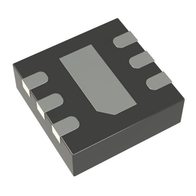
LTC4311
Low Voltage I2C/SMBus
Accelerator
FEATURES
■
■
■
■
■
■
■
■
■
■
■
DESCRIPTION
Improves I2C Bus Rise Time Transition
Ensures Data Integrity with Multiple Devices on the
I2C Bus.
Wide Supply Voltage Range: 1.6V to 5.5V
Improves Low State Noise Margin
Up to 400kHz Operation
Auto Detect Low Power Standby Mode
Low ( VTHR, VCC = 1.8V, 5.5V
●
tr
Fast Mode I2C Bus Rise Time
Bus Capacitance = 400pF, VCC = 3V (Note 4)
●
fMAX
Bus Maximum Operating Frequency
(Note 5)
●
Note 1: Stresses beyond those listed under Absolute Maximum Ratings
may cause permanent damage to the device. Exposure to any Absolute
Maximum Rating condition for extended periods may affect device
reliability and lifetime.
Note 2: All currents into pins are positive. All voltages are referenced to
GND unless otherwise specified.
Note 3: Thermal characteristics are determined with exposed pad soldered
to GND plane. If the exposed pad is left open, thermal characteristics can
be drastically different.
2.5
5
mA
300
400
ns
kHz
Note 4: The rise time of an I2C bus line is calculated from VIL(MAX) to
VIH(MIN) or 0.9V to 2.1V (with VCC = 3V). This parameter is guaranteed by
design and not tested. With a minimum boosted pull-up current of 2.5mA:
Rise Time = (2.1V – 0.9V) • 400pF/2.5mA = 0.19μs.
Note 5: Determined by design, not tested in production.
4311fa
3
�LTC4311
TYPICAL PERFORMANCE CHARACTERISTICS
(TA = 25°C, unless otherwise indicated)
Boost Pull-Up Current vs Bus
Capacitance
Boost Pull-Up Current vs
Temperature
60
RP = 4.7kΩ
CBUS = 1nF
35
30
VCC = 5.5V
25
20
15
10
5
VCC = 3.3V
VCC = 2.5V
40
30
VCC = 3.3V
20
VCC = 2.5V
10
VCC = 1.8V
60
40
20
TEMPERATURE (°C)
0
80
0
100
0
VCC = 1.8V
VCC = 5.5V
VCC = 2.5V
250
VCC = 3.3V
VCC = 3.3V
BUS1 = BUS2 = 0V
RISE TIME (ns)
SUPPLY CURRENT (μA)
5000
4311 G02
300
190
170
160
2000
3000
4000
CAPACITANCE (pF)
Rise Time vs Capacitance
Supply Current vs Temperature
VCC = 2.5V
200
150
VCC = 5.5V
100
150
140
60
40
20
TEMPERATURE (°C)
0
80
0
100
0
2000
3000
4000
CAPACITANCE (pF)
5000
4311 G04
Bus Input Threshold Voltage vs
Supply Voltage
0.8
28
0.75
INPUT THRESHOLD (V)
30
VCC = 5.5V
24
22
1000
4311 G03
Standby Current vs Temperature
26
RP = 2kΩ
Measured from 0.3 • VCC to 0.7 • VCC
50
VCC = 1.8V
130
–40 –20
STANDBY CURRENT (μA)
1000
4311 G01
210
180
VCC = 5.5V
VCC = 1.8V
0
–40 –20
200
Rp = 2kΩ
50
BOOST PULL-UP CURRENT (mA)
BOOST PULL-UP CURRENT (mA)
40
VCC = 3.3V
20
0.7
0.65
0.6
0.55
0.5
VCC = 2.5V
18
0.45
VCC = 1.8V
16
–40 –20
0.4
40
20
60
0
TEMPERATURE (°C)
80
100
4311 G05
1
2
3
4
SUPPLY VOLTAGE (V)
5
6
4311 G06
4311fa
4
�LTC4311
PIN FUNCTIONS
BUS1: Active Pull-up for Bus. Connect to either clock line
or data line for 2-wire bus.
EXPOSED PAD (DFN Package Only): Exposed Pad may
be left open or connected to device ground.
BUS2: Active Pull-up for Bus. Connect to either clock line
or data line for 2-wire bus.
GND: Device Ground. Connect this pin to a ground plane
for best results.
ENABLE: Device Enable Input. This is a 1V nominal digital
threshold input pin. For normal operation drive ENABLE
to a voltage greater than 1.5V. Driving ENABLE below the
0.4V threshold puts the device in a low (
很抱歉,暂时无法提供与“LTC4311CDC#TRMPBF”相匹配的价格&库存,您可以联系我们找货
免费人工找货- 国内价格
- 1+36.05040
- 10+35.20800
- 30+34.64640
- 100+32.72141
